EP0535396A1 - Procédé pour la réduction de fautes de bit dans un système de communication digital - Google Patents
Procédé pour la réduction de fautes de bit dans un système de communication digital Download PDFInfo
- Publication number
- EP0535396A1 EP0535396A1 EP92115202A EP92115202A EP0535396A1 EP 0535396 A1 EP0535396 A1 EP 0535396A1 EP 92115202 A EP92115202 A EP 92115202A EP 92115202 A EP92115202 A EP 92115202A EP 0535396 A1 EP0535396 A1 EP 0535396A1
- Authority
- EP
- European Patent Office
- Prior art keywords
- information
- bit
- elements
- words
- test information
- Prior art date
- Legal status (The legal status is an assumption and is not a legal conclusion. Google has not performed a legal analysis and makes no representation as to the accuracy of the status listed.)
- Ceased
Links
Images

Classifications
-
- H—ELECTRICITY
- H04—ELECTRIC COMMUNICATION TECHNIQUE
- H04L—TRANSMISSION OF DIGITAL INFORMATION, e.g. TELEGRAPHIC COMMUNICATION
- H04L49/00—Packet switching elements
- H04L49/55—Prevention, detection or correction of errors
- H04L49/557—Error correction, e.g. fault recovery or fault tolerance
-
- H—ELECTRICITY
- H04—ELECTRIC COMMUNICATION TECHNIQUE
- H04L—TRANSMISSION OF DIGITAL INFORMATION, e.g. TELEGRAPHIC COMMUNICATION
- H04L1/00—Arrangements for detecting or preventing errors in the information received
- H04L1/22—Arrangements for detecting or preventing errors in the information received using redundant apparatus to increase reliability
-
- H—ELECTRICITY
- H04—ELECTRIC COMMUNICATION TECHNIQUE
- H04L—TRANSMISSION OF DIGITAL INFORMATION, e.g. TELEGRAPHIC COMMUNICATION
- H04L49/00—Packet switching elements
- H04L49/15—Interconnection of switching modules
- H04L49/1515—Non-blocking multistage, e.g. Clos
- H04L49/153—ATM switching fabrics having parallel switch planes
-
- H—ELECTRICITY
- H04—ELECTRIC COMMUNICATION TECHNIQUE
- H04L—TRANSMISSION OF DIGITAL INFORMATION, e.g. TELEGRAPHIC COMMUNICATION
- H04L49/00—Packet switching elements
- H04L49/15—Interconnection of switching modules
- H04L49/1553—Interconnection of ATM switching modules, e.g. ATM switching fabrics
-
- H—ELECTRICITY
- H04—ELECTRIC COMMUNICATION TECHNIQUE
- H04L—TRANSMISSION OF DIGITAL INFORMATION, e.g. TELEGRAPHIC COMMUNICATION
- H04L49/00—Packet switching elements
- H04L49/55—Prevention, detection or correction of errors
- H04L49/552—Prevention, detection or correction of errors by ensuring the integrity of packets received through redundant connections
-
- H—ELECTRICITY
- H04—ELECTRIC COMMUNICATION TECHNIQUE
- H04L—TRANSMISSION OF DIGITAL INFORMATION, e.g. TELEGRAPHIC COMMUNICATION
- H04L69/00—Network arrangements, protocols or services independent of the application payload and not provided for in the other groups of this subclass
- H04L69/40—Network arrangements, protocols or services independent of the application payload and not provided for in the other groups of this subclass for recovering from a failure of a protocol instance or entity, e.g. service redundancy protocols, protocol state redundancy or protocol service redirection
-
- H—ELECTRICITY
- H04—ELECTRIC COMMUNICATION TECHNIQUE
- H04Q—SELECTING
- H04Q11/00—Selecting arrangements for multiplex systems
- H04Q11/04—Selecting arrangements for multiplex systems for time-division multiplexing
-
- H—ELECTRICITY
- H04—ELECTRIC COMMUNICATION TECHNIQUE
- H04Q—SELECTING
- H04Q11/00—Selecting arrangements for multiplex systems
- H04Q11/04—Selecting arrangements for multiplex systems for time-division multiplexing
- H04Q11/0428—Integrated services digital network, i.e. systems for transmission of different types of digitised signals, e.g. speech, data, telecentral, television signals
- H04Q11/0478—Provisions for broadband connections
-
- H—ELECTRICITY
- H04—ELECTRIC COMMUNICATION TECHNIQUE
- H04L—TRANSMISSION OF DIGITAL INFORMATION, e.g. TELEGRAPHIC COMMUNICATION
- H04L12/00—Data switching networks
- H04L12/54—Store-and-forward switching systems
- H04L12/56—Packet switching systems
- H04L12/5601—Transfer mode dependent, e.g. ATM
- H04L2012/5625—Operations, administration and maintenance [OAM]
- H04L2012/5627—Fault tolerance and recovery
Definitions
- the invention is based on a method for bit error reduction in a digital communication system according to the preamble of claim 1, which is known from document DE 38 21 871 C2.
- the analog and digital transmission methods used for data transmission on lines and cables are disruptive influences, e.g. exposed to electromagnetic fields that change the information to be transmitted, e.g. one or more bits are 'flipped' during transmission. Since international long-distance connections in particular are susceptible to bit errors, international standardization bodies - such as CCITT - set minimum requirements for bit error rates. Optical transmission links are subject to these external influences considerably less, so that the transmission security when using optical transmission links is very high.
- these switching matrixes are usually designed to be double or triple. In the event of a switching matrix level malfunctioning, this makes it possible to switch the bit stream through another switching matrix level. This applies in particular in the event of total failure of a switching matrix level.
- Error detection methods for detecting and correcting bit errors in switching matrixes are implemented, for example, in the form of tracking monitoring.
- Such a method is known from German Offenlegungsschrift 24 27 668, in the context of which an additional parity bit is added to the information words per channel defining the information before the actual switching process in the switching matrix, an information word generally consisting of 8 bits.
- a parity bit represents the binary checksum over the individual bits of the corresponding information word or their inversion. After the switching process, the binary checksum of the switched information word is determined again and compared with the transmitted parity bit. If the parity bit transmitted and the newly determined parity bit differ from one another, there is a transmission error which is recorded in a corresponding table memory.
- the invention can be used in switching matrixes which consist of more than two, each actively switched switching matrix levels. What is essential here is the splitting of an information stream consisting of a multiplicity of information words into several, completely identical information streams, as well as a subsequent connection carried out in parallel over each of the respectively switched switching network levels. On the one hand, this enables an evaluation of the parity bits of each switched through information word on the output side, and on the other hand a bit-wise comparison of all information words. Such a combined check generally allows clear conclusions to be drawn about any bit errors that have occurred and allows the forwarding of correct information words to the end user. This results in a very low error rate in the network nodes, a fact that is particularly relevant when using optical transmission links between the network nodes.
- FIG 1 shows a switching matrix SN consisting of 3 switching matrix levels SN0, SN1, SN2 of a digital communication system.
- the switching network levels SN0, SN1, SN2 are connected via interface elements S to the communication network N.
- the interface elements S contain logic elements A, A 'and logic elements B, B'.
- the logic elements A, A 'contain memory elements SP, distributor modules VM and control modules SM are temporarily stored in the memory elements SP.
- a parity bit is formed here.
- the information word is then split together with the parity bit via the distributor modules VM onto the switching network levels SN0, SN1, SN2. This process is controlled and monitored by the control modules SM.
- the switched information words are examined in logic elements B, B 'for bit errors that may have occurred during the switching process.
- they contain memory elements SP, comparator elements VGL, control elements ST and multiplex elements MUX.
- the memory elements SP each carry out a short-term temporary storage of the switched-through information words, followed by a bit-wise difference formation between the separately switched-through information words by the comparator elements VGL and a new parity formation for each information word and switching matrix level; the result of this parity formation is compared with the transmitted parity bit for each switching matrix level. This process is controlled and monitored by control elements ST.
- the information words that are switched through one switching matrix level are compared bit by bit, and on the other hand, an output-side parity test of the 3 information words that are switched through is carried out.
- the result of those evaluations is recorded by statistical evaluation procedures f (s).
- the evaluation procedures f (s) carry statistical data on the quality of the switching operations of the three switching network levels SN0, SN1, SN2. This statistical data is updated in the event of identified and clearly assignable bit errors. In case of doubt, the information word of the switching matrix level is forwarded towards the end user that has had the lowest bit error rate in the past.
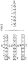
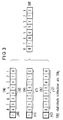
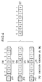
- a particularly simple embodiment of the invention resides in the fact that only the case configurations mentioned under points 1.) and 4.) are taken into account; this means that no static function f (s) is defined. In the exemplary embodiments shown in FIG. 2, FIG. 3, FIG. 4, it is assumed that the information word the length is 8 bits and is saved with the inverted binary checksum as test information.
- bit 4 of the information words I (1) and I (2) routed via the switching network levels SN 1 and SN 2 has been falsified.
- the information word I (o ) is forwarded since parity consistency is present here.
- the information words I (1) , I (2) match, both are inconsistent with regard to their transmitted parity information P.
- bit 4 of the information words I (1) and I (2) routed via the switching network levels SN 1 and SN 2 has been falsified, but additionally bit 3 of the information word I (2) , as a result of which I (2 ) remains consistent with regard to its transmitted parity information.
- one of the information words I (0) or I (2), which are consistent with regard to their transmitted parity information P is carried out as a function of the statistical evaluation procedures f (s).
- the bit error rate of the switching matrix level SN2 was greater than that of the switching matrix level SN0 in the past, the information word I (o) is output in the direction of the end user.
- each bit 4 of the channeled through the switching network levels SN1 and SN2 information words has been tampered with I (1) and I (2), but in addition also to I (2) associated, coassigned parity bit P ( 2) , whereby I (2) remains consistent with its transmitted parity information.
- one of the information words I (o) or I (2), which are consistent with regard to their transmitted parity information is carried out as a function of the statistical evaluation procedure f (s). In particular, if the bit error rate of the switching network levels SN2 was greater than that of the switching network level SN0 in the past, the information word I (o) is output in the direction of the end user.
- the method according to the invention is able to reliably correct single errors in the triple of information words I (o) , I (1) , I (2) , since this is the property of the principle of the majority decision, which is used in such error situations (cf. Process description point 4).
- triple errors in the triple of information words I (o) , I (1) , I (2) which relate to different bit positions, are reliably corrected. If the same bit of all 3 information words I (0) , I (1) , I (2) is falsified, an incorrect output occurs. However, if an information word remains intact in the event of a triple error, the probably correct information word can be output despite the simultaneous falsification of the same bit of the two other information words by using the statistical evaluation procedures f (s) in accordance with points 2.) and 3.) of the method description. This allows the bit errors output to the end user to be further reduced, particularly in the case of switching matrix levels with very different interconnection quality.
- the logic elements A, A ', B, B' can preferably be implemented in a highly integrated component - ASIC component.
- Such modules are used in a variety of ways today; The use of such modules also ensures that the delay times arising in the storage and evaluation of the information words are minimized and can be neglected for practical considerations.
Landscapes
- Engineering & Computer Science (AREA)
- Computer Networks & Wireless Communication (AREA)
- Signal Processing (AREA)
- Computer Security & Cryptography (AREA)
- Detection And Prevention Of Errors In Transmission (AREA)
- Detection And Correction Of Errors (AREA)
Applications Claiming Priority (2)
| Application Number | Priority Date | Filing Date | Title |
|---|---|---|---|
| DE4132552 | 1991-09-30 | ||
| DE4132552A DE4132552C1 (fr) | 1991-09-30 | 1991-09-30 |
Publications (1)
| Publication Number | Publication Date |
|---|---|
| EP0535396A1 true EP0535396A1 (fr) | 1993-04-07 |
Family
ID=6441825
Family Applications (1)
| Application Number | Title | Priority Date | Filing Date |
|---|---|---|---|
| EP92115202A Ceased EP0535396A1 (fr) | 1991-09-30 | 1992-09-04 | Procédé pour la réduction de fautes de bit dans un système de communication digital |
Country Status (3)
| Country | Link |
|---|---|
| US (1) | US5436915A (fr) |
| EP (1) | EP0535396A1 (fr) |
| DE (1) | DE4132552C1 (fr) |
Cited By (2)
| Publication number | Priority date | Publication date | Assignee | Title |
|---|---|---|---|---|
| EP0582848A3 (fr) * | 1992-08-11 | 1995-06-21 | Siemens Ag | Procédé de détection d'erreurs dans des systèmes de communication numériques. |
| FR2737371A1 (fr) * | 1995-07-26 | 1997-01-31 | Trt Telecom Radio Electr | Securisation par doublement d'au moins certaines voies logiques dans un reseau de telecommunications |
Families Citing this family (7)
| Publication number | Priority date | Publication date | Assignee | Title |
|---|---|---|---|---|
| KR100220570B1 (ko) * | 1995-03-16 | 1999-09-15 | 김영환 | 패킷교환기의 에러검출장치 |
| EP0999669A1 (fr) * | 1998-11-06 | 2000-05-10 | Nortel Matra Cellular | Méthode et dispositif de réception en diversité de signaux identiques codés avec des codes correcteurs d'erreurs différents |
| CA2357931A1 (fr) * | 2001-09-27 | 2003-03-27 | Alcatel Canada Inc. | Systeme et methode de selection de sources pour element de reseau a sources redondantes |
| DE60211089T2 (de) * | 2001-09-27 | 2006-11-23 | Alcatel Canada Inc., Ottawa | System und Verfahren zum Auswählen von Datenquellen für ein Netzwerkelement mit redundanten Quellen |
| US7127669B2 (en) * | 2002-05-31 | 2006-10-24 | Kiribati Wireless Ventures, Llc | Redundant path communication methods and systems |
| US9424937B2 (en) * | 2013-02-25 | 2016-08-23 | U.S. Department Of Energy | Method for programming a flash memory |
| CN112073434B (zh) * | 2020-09-28 | 2022-06-07 | 山东产研集成电路产业研究院有限公司 | 降低基于toe的高频交易终端接收通道传输延迟的方法 |
Citations (7)
| Publication number | Priority date | Publication date | Assignee | Title |
|---|---|---|---|---|
| DE2718317A1 (de) * | 1977-04-25 | 1978-11-02 | Gen Electric Co Ltd | Digital koppelnde fernmeldevermittlungseinrichtung |
| WO1985001410A1 (fr) * | 1983-09-12 | 1985-03-28 | Western Electric Company, Inc. | Systeme de commutation double a division temporelle |
| WO1988003738A1 (fr) * | 1986-11-06 | 1988-05-19 | Telefonaktiebolaget L M Ericsson | Procede et reseaux numeriques de commutation servant au controle de defaillances |
| EP0321426A1 (fr) * | 1987-12-18 | 1989-06-21 | Telefonaktiebolaget L M Ericsson | Procédé pour la correction d'erreurs dans un réseau de connexion et réseau de connexion avec dispositif de correction d'erreurs. |
| EP0325318A2 (fr) * | 1988-01-16 | 1989-07-26 | Philips Patentverwaltung GmbH | Central de commutation |
| EP0381104A1 (fr) * | 1989-02-02 | 1990-08-08 | Alcatel Cit | Dispositif de raccordement d'une chaîne centrale de connexion à des unités de raccordement |
| EP0403451A1 (fr) * | 1989-06-16 | 1990-12-19 | Telefonaktiebolaget L M Ericsson | Méthode et dispositif de détection et localisation d'erreurs pour une unité à plusieurs étages dans un commutateur de temps numérique |
Family Cites Families (3)
| Publication number | Priority date | Publication date | Assignee | Title |
|---|---|---|---|---|
| FR2233780B1 (fr) * | 1973-06-13 | 1977-05-06 | Materiel Telephonique | |
| DE3821871A1 (de) * | 1988-06-29 | 1990-01-18 | Philips Patentverwaltung | Breitbandkoppeleinrichtung |
| US5084878A (en) * | 1988-10-24 | 1992-01-28 | Hitachi, Ltd. | Fault tolerant system employing majority voting |
-
1991
- 1991-09-30 DE DE4132552A patent/DE4132552C1/de not_active Expired - Fee Related
-
1992
- 1992-09-04 EP EP92115202A patent/EP0535396A1/fr not_active Ceased
- 1992-09-30 US US07/953,223 patent/US5436915A/en not_active Expired - Fee Related
Patent Citations (7)
| Publication number | Priority date | Publication date | Assignee | Title |
|---|---|---|---|---|
| DE2718317A1 (de) * | 1977-04-25 | 1978-11-02 | Gen Electric Co Ltd | Digital koppelnde fernmeldevermittlungseinrichtung |
| WO1985001410A1 (fr) * | 1983-09-12 | 1985-03-28 | Western Electric Company, Inc. | Systeme de commutation double a division temporelle |
| WO1988003738A1 (fr) * | 1986-11-06 | 1988-05-19 | Telefonaktiebolaget L M Ericsson | Procede et reseaux numeriques de commutation servant au controle de defaillances |
| EP0321426A1 (fr) * | 1987-12-18 | 1989-06-21 | Telefonaktiebolaget L M Ericsson | Procédé pour la correction d'erreurs dans un réseau de connexion et réseau de connexion avec dispositif de correction d'erreurs. |
| EP0325318A2 (fr) * | 1988-01-16 | 1989-07-26 | Philips Patentverwaltung GmbH | Central de commutation |
| EP0381104A1 (fr) * | 1989-02-02 | 1990-08-08 | Alcatel Cit | Dispositif de raccordement d'une chaîne centrale de connexion à des unités de raccordement |
| EP0403451A1 (fr) * | 1989-06-16 | 1990-12-19 | Telefonaktiebolaget L M Ericsson | Méthode et dispositif de détection et localisation d'erreurs pour une unité à plusieurs étages dans un commutateur de temps numérique |
Non-Patent Citations (1)
| Title |
|---|
| PATENT ABSTRACTS OF JAPAN vol. 009, no. 123 (E-317)28. Mai 1985 & JP-A-60 010 996 ( MATSUSHITA ) 21. Januar 1985 * |
Cited By (4)
| Publication number | Priority date | Publication date | Assignee | Title |
|---|---|---|---|---|
| EP0582848A3 (fr) * | 1992-08-11 | 1995-06-21 | Siemens Ag | Procédé de détection d'erreurs dans des systèmes de communication numériques. |
| FR2737371A1 (fr) * | 1995-07-26 | 1997-01-31 | Trt Telecom Radio Electr | Securisation par doublement d'au moins certaines voies logiques dans un reseau de telecommunications |
| EP0757504A1 (fr) * | 1995-07-26 | 1997-02-05 | Philips Communication D'entreprise | Sécurisation par doublement de voies logiques dans un réseau de télécommunications |
| US6580690B1 (en) | 1995-07-26 | 2003-06-17 | Koninklijke Philips Electronics N.V. | Security by doubling at least certain logic paths in a telecommunications network |
Also Published As
| Publication number | Publication date |
|---|---|
| DE4132552C1 (fr) | 1992-11-12 |
| US5436915A (en) | 1995-07-25 |
Similar Documents
| Publication | Publication Date | Title |
|---|---|---|
| DE4128412C1 (fr) | ||
| EP0645913A2 (fr) | Procédé et dispositif pour transmettre des cellules ATM sur des chemins virtuels | |
| DE69829088T2 (de) | Verfahren und Vorrichtung zur Übertragung von Datenrahmen | |
| EP0698980A2 (fr) | Système bus sériel | |
| EP0219917B1 (fr) | Dispositif de commutation avec correction de fautes | |
| DE3614062A1 (de) | Verfahren zur flusssteuerung von daten innerhalb eines vermaschten datennetzes | |
| DE4132552C1 (fr) | ||
| EP0325318B1 (fr) | Central de commutation | |
| DE4226599C2 (de) | Verfahren zur Fehlererkennung in digitalen Kommunikationssystemen | |
| DE69015165T2 (de) | Einrichtung zur Bewertung der Übertragungsqualität. | |
| DE4121481C1 (fr) | ||
| DE4218054C1 (de) | Verfahren zur Mitlaufüberwachung und Bitfehlerreduktion für durchgeschaltete Verbindungen in digitalen Kommunikationssystemen | |
| DE69913152T2 (de) | Ersetzen von Sonderzeichen in einem Datenstrom | |
| EP1886434A1 (fr) | Procede pour transmettre des donnees pour commander un systeme de transmission de courant continu haute tension | |
| EP2388937B1 (fr) | Procédé de transmission d'un signal numérique en multiplexe inverse, notamment par un réseau de transport optique et dispositif de réception pour un système destiné à la réalisation du procédé | |
| EP0999675B1 (fr) | Circuit détecteur de défauts de lignes pour système de transmission de données électriques | |
| EP0353660B1 (fr) | Procédé de protection contre les fautes dans les systèmes à mémoires d'installation de traitement de données, en particulier les installations de centraux téléphoniques | |
| DE2915113A1 (de) | Busvorrichtung fuer ein datenverarbeitendes system | |
| EP0402741B1 (fr) | Méthode et dispositif pour la retransmission des cellules transmises en mode de transfert asynchrone | |
| WO1993000760A1 (fr) | Procede de determination de l'origine d'erreurs sur les bits | |
| DE19626064A1 (de) | Einrichtung zur Behebung von Fehlern in einem Kontrollblock für eine Kopfstelle und zugehöriges Prüfverfahren | |
| CH674689A5 (fr) | ||
| DE69631366T2 (de) | Verfahren und Vorrichtung zur Korrektur von Übertragungsfehlern und Erkennung von Fehlern während der Übertragung von Daten über ein Datenübertragungsmedium | |
| DE19836254A1 (de) | Verfahren zum Aktivieren und Deaktivieren der Quelle bzw. der Senke einer Tandemverbindung in einem Telekommunikationsnetzwerk sowie Quelle und Senke einer solchen Tandemverbindung | |
| EP1680895A2 (fr) | Syst me de transmission de donn es dans un bus s riel bidirectionnel |
Legal Events
| Date | Code | Title | Description |
|---|---|---|---|
| PUAI | Public reference made under article 153(3) epc to a published international application that has entered the european phase |
Free format text: ORIGINAL CODE: 0009012 |
|
| AK | Designated contracting states |
Kind code of ref document: A1 Designated state(s): CH DE FR GB IT LI SE |
|
| 17P | Request for examination filed |
Effective date: 19930422 |
|
| 17Q | First examination report despatched |
Effective date: 19960917 |
|
| GRAG | Despatch of communication of intention to grant |
Free format text: ORIGINAL CODE: EPIDOS AGRA |
|
| 18R | Application refused |
Effective date: 19981119 |