EP0325408A2 - Halbleiteranordnung mit einer Verbindungsschicht - Google Patents
Halbleiteranordnung mit einer Verbindungsschicht Download PDFInfo
- Publication number
- EP0325408A2 EP0325408A2 EP89300405A EP89300405A EP0325408A2 EP 0325408 A2 EP0325408 A2 EP 0325408A2 EP 89300405 A EP89300405 A EP 89300405A EP 89300405 A EP89300405 A EP 89300405A EP 0325408 A2 EP0325408 A2 EP 0325408A2
- Authority
- EP
- European Patent Office
- Prior art keywords
- ceramic
- semiconductor device
- interconnection portions
- interconnection
- superconducting
- Prior art date
- Legal status (The legal status is an assumption and is not a legal conclusion. Google has not performed a legal analysis and makes no representation as to the accuracy of the status listed.)
- Withdrawn
Links
Images
Classifications
-
- H—ELECTRICITY
- H10—SEMICONDUCTOR DEVICES; ELECTRIC SOLID-STATE DEVICES NOT OTHERWISE PROVIDED FOR
- H10W—GENERIC PACKAGES, INTERCONNECTIONS, CONNECTORS OR OTHER CONSTRUCTIONAL DETAILS OF DEVICES COVERED BY CLASS H10
- H10W20/00—Interconnections in chips, wafers or substrates
- H10W20/40—Interconnections external to wafers or substrates, e.g. back-end-of-line [BEOL] metallisations or vias connecting to gate electrodes
- H10W20/41—Interconnections external to wafers or substrates, e.g. back-end-of-line [BEOL] metallisations or vias connecting to gate electrodes characterised by their conductive parts
- H10W20/44—Conductive materials thereof
- H10W20/4484—Superconducting materials
Definitions
- the present invention relates to a semiconductor device, more particularly it relates to a semiconductor device wherein an interconnection layer or portion consists of high temperature superconducting material.
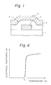
- Figure 1 is a cross-sectional view explaining a conventional process for forming an interconnection.
- an aluminium (Al) interconnection or wiring 2 is formed on a substrate 1 and an insulating layer 3 of phosphorus silicate glass (PSG) is deposited over the entire surface of the substrate 1.
- PSG phosphorus silicate glass
- planarization to reduce the step 4 often leads to a break in the PSG layer at step 4, which results in a short-circuit between the interconnection 2 and the other interconnection 5 at the step 4. Furthermore, due to the differences in the thermal expansion coefficients of the aluminium interconnection 2 and the PSG layer 3, stress occurs and thus the problem of a migration of aluminium arises.
- An object of the present invention is to provide a semiconductor device wherein an interconnection or wiring can be easily formed, which interconnection may be conveniently formed as a three dimensional interconnection.
- a semiconductor device comprising: interconnection portions consisting of a ceramic superconducting material and a portion positioned between said interconnection portions and having much of the composition of said interconnection portions but acting as an electrical insulator with respect to the interconnection portion at temperatures at which the latter are electrically conducting.
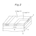
- an insulating layer 9 such as a silicon dioxide (SiO2) layer is formed on a silicon substrate 8, and openings (not shown) are provided to connect the diffusion layer of the surface of the silicon substrate 8 to an interconnection portion (wiring) as required.
- a thin film A having much of the composition of a ceramic superconducting material is formed on the entire surface of the insulating layer 9, with a key composition generating the superconducting property being contained in only the interconnection portions 13 of the thin film A.
- the other portion 14 of the thin film A has much the same composition as that of the interconnection portions 13.
- the interconnection portions 13 are however electrically insulated by the portion 14.
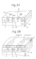
- Figures 3A and 3B are perspective views explaining an embodiment of an interconnection portion of a semiconductor device according to the present invention.
- N+ source and drain regions 11 and 12 are formed on a silicon dioxide (SiO2) layer 10, and a P channel region 15 is provided between the N+ source and drain regions 11 and 12.
- the SiO2 layer 16 is an isolation region.
- An SiO2 layer 17 is deposited on the source and drain regions 11 and 12, and is provided with source contacts 18 and drain contacts 19.
- a thin film A having much of the composition of a ceramic superconducting material is formed as shown in Figure 3B.
- a key composition for the generation of a superconductivity at a high temperature, for example, liquid nitrogen temperature, is contained in only an interconnection portion 13 of the thin film.
- a portion 14 between the interconnection portion 13 consist of ceramics containing much of the composition of the interconnection portion 13, but not showing a superconductive property or showing this property only at a very low temperature.
- the interconnection portion 13 containing the key composition by which above-mentioned superconduction is generated consists of, for example, an M-L-A-O system ceramic high-temperature super-conducting material, wherein M is an alkaline earth metal such as calcium (Ca), strontium (Sr), or a combination of alkaline earth metals, and L is a rare earth element such as yttrium (Y) or lanthanum (La), or a heavy element such as bismuth (Bi) or thallium (Tl) also known as a component of such material able to replace a rare earth element, or a combination of such elements, and A is Cu, Ag or Au or a combination thereof.
- M is an alkaline earth metal such as calcium (Ca), strontium (Sr), or a combination of alkaline earth metals
- L is a rare earth element such as yttrium (Y) or lanthanum (La), or a heavy element such as bismuth (Bi) or
- the insulating portion 14 which does not show the superconductive property, or even if such a property is shown, it appears only at a very low temperature such as 4.2 K or less, has a composition in which one of the characteristic metals of superconducting interconnection portion 13 is omitted to leave a ceramic composition otherwise the same as that of interconnection portion 14 and generally acting as an insulator at temperatures well below the transition temperature Tc of portion 13.
- L is not present (i.e., M-A-O system material).
- the ceramic superconductive material used in the present invention is an oxide ceramic material represented by the general formula X a Y 1-a ZO b or (X 1-a Y a )2ZO b where 0 ⁇ a ⁇ 1; 3 ⁇ b ⁇ 4;
- X is at least one element selected from the group of Ba, Ca, Sr, and Mg;
- Y is at least one element selected from the group of Sc, Y, La, Ce, Pr, Nd, Pm, Sm, Eu, Gd, Tb, Dy, Ho, Er, Tm, Yb, and Lu;
- Z is at least one element selected from the group of Cu, Ag, and Au.
- X, Y, and Z in the above formula may be more than one element.
- X may be Ba-Ca-Sr, Ba-Ca-Mg, Ba-Ca, or Ca-Mg
- Y may be Sc-Y, Sc-Y-La, Sc-Y-La-Ce, or Pr-Nd and, Z may be Cu-Ag, Cu-Au, Ag-Au, or Cu-Ag-Au.
- the oxide superconductive material may be, for example, (Ba 0.6 Ca 0.2 Sr 0.2 ) 0.6 (Sc 0.7 Y 0.2 La 0.1 ) 0.4 (Cu 0.8 Ag 0.2 )3O 4-w or (Ba 0.8 Mg 0.2 ) 0.7 (Sc 0.6 Nd 0.4 ) 0.3 Cu3O 4- ⁇ .
- a preferred oxide superconductive material is ⁇ (M II O) x (M III O3) 1-x ⁇ y (CuO) z (O) ⁇
- M II stands for at least one of Ba, Sr, Ca, and Mg
- M III stands for at least one of Y, Sc, La, Ce, Pr, Nd, Sm, Eu, Gd, Tb, Dy, Ho, Er, Tm, Tb, and Lu
- ⁇ stands for a deviation of the amount of oxygen from stoichiometry; the oxide superconducting material exhibiting superconductivity above the boiling point of nitrogen (77K).
- a superconducting ceramic material is a bismuth-system (Bi-Sr-Ca-Cu-O system) superconducting ceramic material.
- the exact chemical formula of the bismuth-system superconducting ceramic material is not known but can be formed from a starting material of a mixture of Bi, Sr, Ca, and Cu compounds in a molar ratio (based on these elements) of 0.25-2:0.1-5:0.1-5:0.5-4. For example, 1:1:1:2; 1:1:1:3, 4:3:3:6; and 4:3:3:4.
- another superconducting ceramic material can be formed from a starting material of a mixture of Tl, Bi, Sr, Ca, and Cu compounds in a molar ratio (based on these elements) of 0.25-2:0.25-2:0.1-5:0.1-5:0.5-4. These superconducting ceramic materials exhibit superconductivity above the boiling point of nitrogen (77K).
- the insulating portion 14 generally has the same thickness as that of the interconnection portion 13.
- CuO and BaCO3 powders were mixed so that the mol composition ratio Ba:Cu:O was 1:1.5:3.5, and heated or calcined at a temperature of about 950°C for 10 hours in air.
- the calcined lumps were again powdered, remixed, and pressed to form a wafer-shaped body having a diameter of 100 cm and a thickness of 5 mm, at a pressure of 500 kg/cm2, and reheated or sintered at a temperature of 950°C for 5 hours in an oxygen (O2) gas atmosphere.
- O2 oxygen
- a planner type RF magnetron sputtering was carried out, using the above-mentioned target, at a deposition rate of about 6 nm/min, in an atmosphere of Ar and 50% O2, at a pressure of 2 to 3 Pa, and at a substrate temperature of 500 to 600°C.
- the thickness of the obtained Ba-Cu-O thin film was about 500 nm.
- Y+ yttrium ions
- FIB focussed ion beam
- the obtained thin film was annealed at an energy density of 20 W/cm2, a scan speed of 5 cm/sec, with a beam spot having a 100 ⁇ m diameter, and in an O2 atmosphere.
- the substrate was kept at a temperature of 500 to 600°C during the laser-irradiation, and the irradiated spot of the laser was estimated to have a temperature of 1230 to 1250°C, which is near the melting point of the Y1Ba2Cu3 O 7-x .
- the thus-obtained interconnection portions 13 became superconductive at a critical temperature of 90K, and a Ba-Cu-O thin film portion 14 not implanted by Y maintained an insulative effect at 5K or higher.
- a disc or wafer shaped target of La.Ba.Sr.O3 was produced in the same way as in Example 1, and Cu+ ions were then implanted only intointerconnecting portions by the FIB process, under the implantation conditions of a dose of 6 to 9 x 1017 cm ⁇ 2 and at an energy of 100 KeV. Further, O+ ions were implanted therein at a high dose of 2 to 3 x 1017 cm ⁇ 2 and an energy of 100 KeV, as the thin film was to be encapsulated by SiO2/Poly-Si for a later laser annealing process and the supply of O2 from the atmosphere was lost.
- a 500 nm thick SiO2 and 400 nm thick non doped poly-Si were deposited on a ceramic thin film by a low pressure CVD process, and the surface of the film was then irradiated with a CW Ar+ laser under the conditions of an energy density of 20 W/cm2, a scan speed of 5 cm/sec, and a beam spot diameter of 100 ⁇ m, so that the poly-Si was melted and recrystallized, and then only the Si layer was removed by etching.
- a field portion Ba.Ca.Cu.Ox ceramic was formed by an RF sputtering target as in Example 1, and after a Bi+ ion implantation at a dose of 2 to 3 x 1017 cm ⁇ 3, the surface of the ceramic was irradiated with a CO2 laser in an O2 flow, as in Example 1.
- the field portion had a Tc of lower than 4.2K (Tc ⁇ 4.2K).
- the interconnection portion can be easily planarized without a pattern-etching of the thin film, or PSG reflow. Further, since the interconnection portion 13 and the portion 14 have substantially the same ceramic composition, the thermal expansion therebetween is substantially the same, and thus stress does not occur.
Landscapes
- Internal Circuitry In Semiconductor Integrated Circuit Devices (AREA)
- Superconductors And Manufacturing Methods Therefor (AREA)
- Superconductor Devices And Manufacturing Methods Thereof (AREA)
- Compositions Of Oxide Ceramics (AREA)
Applications Claiming Priority (2)
| Application Number | Priority Date | Filing Date | Title |
|---|---|---|---|
| JP63006830A JPH01183138A (ja) | 1988-01-18 | 1988-01-18 | 半導体装置 |
| JP6830/88 | 1988-01-18 |
Publications (2)
| Publication Number | Publication Date |
|---|---|
| EP0325408A2 true EP0325408A2 (de) | 1989-07-26 |
| EP0325408A3 EP0325408A3 (de) | 1989-09-06 |
Family
ID=11649141
Family Applications (1)
| Application Number | Title | Priority Date | Filing Date |
|---|---|---|---|
| EP89300405A Withdrawn EP0325408A3 (de) | 1988-01-18 | 1989-01-17 | Halbleiteranordnung mit einer Verbindungsschicht |
Country Status (3)
| Country | Link |
|---|---|
| EP (1) | EP0325408A3 (de) |
| JP (1) | JPH01183138A (de) |
| KR (1) | KR910009358B1 (de) |
Cited By (3)
| Publication number | Priority date | Publication date | Assignee | Title |
|---|---|---|---|---|
| EP0457468A3 (en) * | 1990-05-14 | 1992-04-08 | American Telephone And Telegraph Company | Integrated electronic assembly comprising a transmission line |
| WO1993000708A1 (de) * | 1991-06-24 | 1993-01-07 | Forschungszentrum Jülich GmbH | Strukturierte leiterbahnen und verfahren zur herstellung derselben |
| US6156513A (en) * | 1995-09-15 | 2000-12-05 | Ramareddy V. Guntaka | Oligmers which inhibit expression of collagen genes |
Families Citing this family (2)
| Publication number | Priority date | Publication date | Assignee | Title |
|---|---|---|---|---|
| JPH0355889A (ja) * | 1989-07-25 | 1991-03-11 | Furukawa Electric Co Ltd:The | 超電導多層回路の製造方法 |
| JPH0371147U (de) * | 1989-11-13 | 1991-07-18 |
Family Cites Families (1)
| Publication number | Priority date | Publication date | Assignee | Title |
|---|---|---|---|---|
| EP0282012A3 (de) * | 1987-03-09 | 1989-09-13 | Semiconductor Energy Laboratory Co., Ltd. | Supraleitende Halbleiteranordnung |
-
1988
- 1988-01-18 JP JP63006830A patent/JPH01183138A/ja active Pending
-
1989
- 1989-01-17 EP EP89300405A patent/EP0325408A3/de not_active Withdrawn
- 1989-01-18 KR KR8900486A patent/KR910009358B1/ko not_active Expired
Cited By (3)
| Publication number | Priority date | Publication date | Assignee | Title |
|---|---|---|---|---|
| EP0457468A3 (en) * | 1990-05-14 | 1992-04-08 | American Telephone And Telegraph Company | Integrated electronic assembly comprising a transmission line |
| WO1993000708A1 (de) * | 1991-06-24 | 1993-01-07 | Forschungszentrum Jülich GmbH | Strukturierte leiterbahnen und verfahren zur herstellung derselben |
| US6156513A (en) * | 1995-09-15 | 2000-12-05 | Ramareddy V. Guntaka | Oligmers which inhibit expression of collagen genes |
Also Published As
| Publication number | Publication date |
|---|---|
| KR910009358B1 (en) | 1991-11-12 |
| JPH01183138A (ja) | 1989-07-20 |
| KR890012376A (ko) | 1989-08-26 |
| EP0325408A3 (de) | 1989-09-06 |
Similar Documents
| Publication | Publication Date | Title |
|---|---|---|
| EP0307147B1 (de) | Halbleiteranordnungen mit supraleitenden Verbindungen | |
| US4316785A (en) | Oxide superconductor Josephson junction and fabrication method therefor | |
| EP0286106B1 (de) | Verfahren zur Herstellung eines supraleitenden Elements | |
| CA1332326C (en) | Preparation of superconducting oxide films on silicon and silicon dioxide substrates | |
| JPH0634418B2 (ja) | 超電導素子の作製方法 | |
| CA1314109C (en) | Barrier layer superconductive device | |
| EP0327493B1 (de) | Epitaxische Anordnung von Hochtemperatur-Supraleitern | |
| EP0277749A2 (de) | Supraleitendes Oxid | |
| EP0282012A2 (de) | Supraleitende Halbleiteranordnung | |
| EP0341148B1 (de) | Halbleitersubstrat mit dünner Supraleiterschicht | |
| US5283465A (en) | Superconducting lead on integrated circuit | |
| US5401716A (en) | Method for manufacturing superconducting patterns | |
| JP3120742B2 (ja) | 超伝導回路及びその製造方法 | |
| US5389603A (en) | Oxide superconductors, and devices and systems comprising such a superconductor | |
| US5332722A (en) | Nonvolatile memory element composed of combined superconductor ring and MOSFET | |
| EP0470806B1 (de) | Aktive Einrichtung mit oxydischem Supraleiter und deren Herstellungsprozess | |
| EP0488837B1 (de) | Verfahren zur Herstellung einer supraleitenden Einrichtung mit reduzierter Dicke der supraleitenden Schicht und dadurch erzeugte supraleitende Einrichtung | |
| JP3425422B2 (ja) | 超電導素子の製造方法 | |
| JPH0272685A (ja) | 超伝導弱結合部の形成方法 | |
| JPH01183138A (ja) | 半導体装置 | |
| JP2579335B2 (ja) | 超伝導体素子の製造方法 | |
| KR930004024B1 (ko) | 초전도 집적회로소자의 제조방법 | |
| JP2559413B2 (ja) | 酸化物超電導集積回路 | |
| JP2899287B2 (ja) | ジョセフソン素子 | |
| JPH0284732A (ja) | 超伝導体素子の製造方法 |
Legal Events
| Date | Code | Title | Description |
|---|---|---|---|
| PUAI | Public reference made under article 153(3) epc to a published international application that has entered the european phase |
Free format text: ORIGINAL CODE: 0009012 |
|
| PUAL | Search report despatched |
Free format text: ORIGINAL CODE: 0009013 |
|
| AK | Designated contracting states |
Kind code of ref document: A2 Designated state(s): DE FR GB |
|
| AK | Designated contracting states |
Kind code of ref document: A3 Designated state(s): DE FR GB |
|
| 17P | Request for examination filed |
Effective date: 19900302 |
|
| 17Q | First examination report despatched |
Effective date: 19911008 |
|
| STAA | Information on the status of an ep patent application or granted ep patent |
Free format text: STATUS: THE APPLICATION IS DEEMED TO BE WITHDRAWN |
|
| 18D | Application deemed to be withdrawn |
Effective date: 19930409 |