EP0325765A1 - Dispositif josephson ayant une structure josephson utilisable pour un supraconducteur d'oxyde - Google Patents
Dispositif josephson ayant une structure josephson utilisable pour un supraconducteur d'oxyde Download PDFInfo
- Publication number
- EP0325765A1 EP0325765A1 EP88121155A EP88121155A EP0325765A1 EP 0325765 A1 EP0325765 A1 EP 0325765A1 EP 88121155 A EP88121155 A EP 88121155A EP 88121155 A EP88121155 A EP 88121155A EP 0325765 A1 EP0325765 A1 EP 0325765A1
- Authority
- EP
- European Patent Office
- Prior art keywords
- crystal
- superconductor
- josephson
- film
- josephson device
- Prior art date
- Legal status (The legal status is an assumption and is not a legal conclusion. Google has not performed a legal analysis and makes no representation as to the accuracy of the status listed.)
- Granted
Links
Images
Classifications
-
- H—ELECTRICITY
- H10—SEMICONDUCTOR DEVICES; ELECTRIC SOLID-STATE DEVICES NOT OTHERWISE PROVIDED FOR
- H10N—ELECTRIC SOLID-STATE DEVICES NOT OTHERWISE PROVIDED FOR
- H10N60/00—Superconducting devices
- H10N60/10—Junction-based devices
- H10N60/12—Josephson-effect devices
- H10N60/124—Josephson-effect devices comprising high-Tc ceramic materials
-
- H—ELECTRICITY
- H10—SEMICONDUCTOR DEVICES; ELECTRIC SOLID-STATE DEVICES NOT OTHERWISE PROVIDED FOR
- H10N—ELECTRIC SOLID-STATE DEVICES NOT OTHERWISE PROVIDED FOR
- H10N60/00—Superconducting devices
- H10N60/01—Manufacture or treatment
- H10N60/0268—Manufacture or treatment of devices comprising copper oxide
- H10N60/0296—Processes for depositing or forming copper oxide superconductor layers
- H10N60/0576—Processes for depositing or forming copper oxide superconductor layers characterised by the substrate
- H10N60/0604—Monocrystalline substrates, e.g. epitaxial growth
-
- H—ELECTRICITY
- H10—SEMICONDUCTOR DEVICES; ELECTRIC SOLID-STATE DEVICES NOT OTHERWISE PROVIDED FOR
- H10N—ELECTRIC SOLID-STATE DEVICES NOT OTHERWISE PROVIDED FOR
- H10N60/00—Superconducting devices
- H10N60/01—Manufacture or treatment
- H10N60/0912—Manufacture or treatment of Josephson-effect devices
- H10N60/0941—Manufacture or treatment of Josephson-effect devices comprising high-Tc ceramic materials
Definitions
- the present invention relates to a Josephson device and, more particularly, to a Josephson device having a Josephson junction structure suitable for an oxide superconductor.
- a Josephson device having a metal superconductor, such as niobium, or an intermetallic compound superconductor, such as niobium nitride has hitherto been realized by forming a tunnel barrier with an insulator or a semiconductor, such as aluminum oxide or germanium, between the two superconductors to form a Josephson junction.
- oxide compounds such as a Y-Ba-Cu-O compound, which exhibit superconducting properties.
- Oxide superconductors of this kind exhibit a transition into a superconducting state at a relatively high absolute temperature of about 40 to 90K.
- the superconducting characteristics, i.e., physical constants such as critical current density, critical magnetic field, and coherence length, of these high-temperature oxide superconductors greatly depend upon the crystal orientation, and show a great difference of more than ten times in those superconducting properties between the C-axis direction and the direction orthogonal to the C-axis.
- These high-temperature oxide superconductors have a remarkably small coherence length of about 2 to 4 nm and tends to bring about breakdown of the superconductivity originated in an oxygen elimination in vacuo and a reaction with steam in the air. For this reason, it was very difficult to form a Josephson junction between these oxide superconductors by inserting an insulator or a semiconductor therebetween.
- a thin film of a high temperature oxide superconductor exhibits superconducting properties without annealing when formed on a magnesia (MgO) or strontium titanate (SrTiO3) crystal at a substrate temperature of 500 to 700°C with a crystal orientation determined by that of the substrate.
- MgO magnesia
- SrTiO3 strontium titanate
- a Josephson device with a high-temperature oxide superconductor can be prepared by a process wherein a crack is formed in an oxide superconductor ceramic rod to develop minute weak bonds within the rod (see "Japanese Journal of Applied Physics", Vo. 26, No. 5, pp. L701-L703) or a process in which a film is formed on a strontium titanate or magnesia substrate and annealing is then conducted to give a grain boundary for use as a Josephson junction (see "Technical Report of Institute of Electronics, Information and Communication Engineers, SCE87-38, vol. 87, No. 249, pp. 73-78). Furthermore, there has been developed a SQUID which was a grain boundary formed within an oxide superconductor film as a Josephson device.
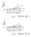
- Japanese Published Unexamined Patent Application No. 62-273782 discloses a process for preparing a grain boundary within a BaPb 1-x Bi x O3 film of an oxide superconductor. Schematic cross-sectional views of structures of grain boundary junctions in BaPb 1-x Bi x O3 (hereinafter abbreviated to "BPB") films are shown in Figs. 1 and 2.
- a step 31 is formed on the (100) surface of a strontium titanate substrate 1, and a BPB film 32 is then grown along the C-axis direction on the whole surface of the substrate 1 to selectively grow crystal layers on both sides of the step 31.
- the BPB film 32 is grown to have a thickness exceeding the height of the step 31, the crystal layers on both sides of the step 31 contact with each other to form a grain boundary therebetween, resulting in forming a Josephson junction 5.
- a chromium film slit 33 having a width of a few microns is formed on a (100) strontium titanate substrate 1, and a BPB film 32 is then grown along the C-axis direction on the whole surface of the substrate 1.
- the chromium film slit 33 is formed to have a sufficiently small width, and the BPB film 32 is grown so as to have a thickness exceeding that of the chromium film slit 33.
- the BPB film 32 has a sufficient thickness, the crystal layers on both sides of the chromium film slit 33 are brought into contact with each other on the slit 33 through a grain boundary, thereby forming a Josephson junction 5.
- the operational switching speed is nearly proportional to the reciprocal of the current density at the Josephson junction.
- the area of the Josephson junction parallel to the C-axis was necessarily smaller than the thickness of the superconductor film 32, resulting in making it impossible to form a Josephson junction of a large current density, since the current density orthogonal to the C-axis is at least ten times larger than that parallel to the C-axis.
- the Josephson device in accordance with the present invention includes a crystal region having a distorted or broken lattice in a main surface of a crystal substrate or a crystal film, a superconductor film grown on the crystal substrate or the crystal film, and a crystal boundary formed in the superconductor film at a portion on the crystal region, thereby forming a Josephson junction.
- the Josephson junction of the present invention can be manufactured by implanting accelerated ions into the crystal substrate or the crystal film to distort or break the crystal lattice and to form the above-described crystal region of the distorted or broken lattice.
- chemically stable materials such as gold and platinum, as the ion-implanted ions.
- the distorted or broken-lattice crystal region is first formed in a main surface of the crystal substrate or the crystal film on which a film of a superconducting material, such as a high-temperature oxide superconductor, is to be formed. Thereafter, the film of the super conducting material is formed thereon.
- the crystal structure of the crystal substrate is reflected in that of the superconductor thin film formed thereon. Therefore, the crystal structure in the superconductor film is unsettled on the distorted or broken-lattice crystal region, which suppresses the crystallization of the superconductor film.
- the crystal region of the superconductor film grown on both sides of the distorted or broken-lattice crystal region is gradually extended to the portion over the distorted or broken-lattice crystal region, to form the superconductor film having a crystal boundary only at the portion on the distorted or broken-lattice crystal region.
- the Josephson device of the present invention is a device wherein a crystal boundary formed by the above-described process is used as a Josephson junction. Therefore, the position and dimension of the Josephson junction can be easily determined with high accuracy by controlling the distorted or broken-lattice region formed on the substrate crystal and the thickness or the superconducting film, resulting in stabilizing the electrical characteristics. Moreover, since the surface of the device of the present invention is flat, a desired circuit element can be formed on the device of the present invention. ⁇
- the superconductor film is formed flat at the portion over the distorted or broken-lattice crystal region of the crystal substrate to make the area of the Josephson junction equal to the section area of superconducting film and the crystal orientation of this superconductor film can be determined by the crystal orientation of the substrate, it is possible to form a Josephson device allowing a current flow of a large current density.
- the Josephson device includes a distorted or broken-lattice crystal region 2 formed in the main the surface of a strontium titanate (SrTiO3) single crystal substrate 1, first and second superconductor electrodes 3, 4 of yttrium-barium-copper oxides, and a Josephson junction 5 composed of a crystal boundary formed between the first superconductor electrodes 3 and the second superconductor electrode 4.
- a single crystal having a plane orientation (100) is used as the strontium titanate crystal substrate 1.
- the yttrium-barium-copper oxide superconductor films constituting the first and second superconductor electrodes 3, 4 have a plane orientation (100) which is the same plane orientation as that of the substrate 1. Therefore, a current passing through the Josephson junction 5 flows in the direction orthogonal to the C-axis of the yttrium-barium-copper oxide superconductor films constituting the first and second superconductor electrodes 3, 4, which makes it possible to attain a Josephson junction with a current density of at least 106 A/cm2.
- sufficiently large critical current value of a Josephson device i.e., at least 0.1 mA, can be easily attained by a Josephson device with a superconductor film having a line width of 1 ⁇ m and a thickness of 0.2 ⁇ m.
- This Josephson device is manufactured as follows. At the outset, gold (Au) ions having a beam diameter of 0.2 ⁇ m and accelerated by applying a voltage of 100 kV according to the focused ion beam method are implanted into a surface portion of a strontium titanate crystal (SrTiO3) substrate 1 having the plane orientation (100) on which a Josephson device is to be formed. Part of the crystal structure or the lattice structure of the strontium titanate substrate 1 is broken by the gold ion implantation, which forms the distorted or broken-lattice crystal region 2.
- the (100) strontium titanate single crystal substrate 1 is heated to 650°C to grow the crystal of the yttrium-barium-copper oxide (YBa2Cu3O7- ⁇ ) at a growth rate of 10 nm/min.
- Sintered yttrium-barium-copper oxide is heated and evaporated to grow the yttrium-barium-copper oxide film with electron beams accelerated by applying a voltage of 10 kV.
- the first and second superconductor electrodes 3, 4 are formed by growing yttrium-barium-copper oxide for 30 minutes under the above-described condition.
- the films of superconductor electrodes 3, 4 respectively have a crystal plane orientation (100), i.e., the same crystal plane orientation as that of the strontium titanate substrate 1.
- the single crystal of the first superconductor electrode 3 is grown from the left-hand side of the distorted or broken-lattice crystal retion 2, whereas the single crystal of the second superconductor electrode 4 is grown from the right-hand side of the distorted or broken-lattice crystal region 2. Therefore, a crystal boundary 5 between the first and second superconductor electrodes 3 and 4 is formed on the distorted or broken-lattice crystal region 2 of the substrate 1.
- the first and second electrodes 3 and 4 are worked into a desired shape, e.g., a 4 ⁇ m-width by exposure and etching techniques, and subjected to necessary wiring to form a Josephson device.
- the yttrium-barium-copper oxide film is etched by a reactive ion beam etching method wherein a chlorine gas of 10 ⁇ 3 Torr is ionized with a high-frequency plasma and then accelerated by applying a draw-out voltage of 400 V.
- the etching is conducted at a rate of 4 nm/min for 80 min, to pattern the superconductor electrodes 3, 4.
- the superconductor films 3 and 4 may also be formed by the known film forming techniques besides the above-described process, such as D.C. sputtering and A.C. sputtering wherein an electrode of a sintered superconductor such as an yttrium-barium-copper oxide is used or a process wherein three yttrium, barium and copper electrodes are sputtered or evaporated simultaneously or in a time-sharing manner. Ion beam etching, reactive plasma etching wherein a gas other than chlorine is used, or the like may be used for working the superconductor film.
- a sintered superconductor such as an yttrium-barium-copper oxide
- Ion beam etching, reactive plasma etching wherein a gas other than chlorine is used, or the like may be used for working the superconductor film.
- the superdoncutror film forming temperature may be other than 650°C and, if necessary, may be varied in a range from 400 to 900°C. Further, it is known that magnesia (MgO) and sapphire can also be used as the substrate.
- MgO magnesia
- sapphire can also be used as the substrate.
- a strontium titanate crystal (SrTiO3) film 22 is formed on a (100) sapphire crystal substrate 21.
- Sapphire is used as the substrate because a high-quality crystal substrate can be prepared therefrom at low cost.
- the strontium titanate film 22 is formed on the sapphire substrate 21 at a rate of 10 nm/min for 20 min to have a thickness of 200 nm according to the electron beam deposition or the like.
- the strontium titanate film 22 thus prepared is a single crystal having a plane orientation (100).
- the first and second superconductor electrodes 3, 4 are then formed.
- the superconductor electrodes 3, 4 are prepared by forming a 300 nm-thick film of an yttrium-barium-copper oxide, a lanthanum-strontium-copper oxide [(La 1-x Sr x )2CuO4)], or the like.
- the heating of the substrate at a temperature of 600°C and irradiating of pure oxygen against the surface of the sample cause single crystal superconductors each having a plane orientation (100) to grow, resulting in the superconductor electrodes 3, 4.
- the oxygen pressure on the surface of the sample is set at 10 to 100 Pa.
- a crystal boundary is formed on the distorted or broken-lattice crystal region 2 in the strontium titanate film.
- a Josephson device having a crystal boundary as the Josephson junction 5 and superconductor electrodes 3, 4.
- the distorted or broken-lattice crystal region 2, electrodes 3, 4 and Josephson junction 5 in this second embodiment may be prepared in the same manner as that of the first example.
- a superconductor film formed on a single crystal substrate having a plane orientation (100) or on a crystal film having a plane orientation (100) according to the above-described first or second embodiments is easily grown in the form of a crystal having a plane orientation (100). Since the superconducting electrodes 3 and 4 are grown along ⁇ 100> direction (i.e., C-axis direction), the Josephson junction is formed in parallel with the C-axis. Since the current density in the direction orthogonal to the C-axis is at least ten times larger than that of C-axis, the Josephson junction with large current density can be formed, resulting in the large critical current value.
- the crystal film used as the underlayer on which a superconductor film is formed may also be other material than those described above, such as magnesia (MgO). It is apparent that various known combinations of substrates with crystal films can be utilized as other structures of the Josephson device wherein a crystal film is used as the underlayer on which a superconductor film is to be formed. For example, it is possible to use a Si substrate having a sapphire single crystal film formed on the surface thereof or a sapphire substrate having a SrTiO3 film formed on the surface thereof.
Landscapes
- Engineering & Computer Science (AREA)
- Chemical & Material Sciences (AREA)
- Ceramic Engineering (AREA)
- Manufacturing & Machinery (AREA)
- Crystallography & Structural Chemistry (AREA)
- Superconductor Devices And Manufacturing Methods Thereof (AREA)
Applications Claiming Priority (2)
| Application Number | Priority Date | Filing Date | Title |
|---|---|---|---|
| JP62320516A JPH01161881A (ja) | 1987-12-18 | 1987-12-18 | ジョセフソン素子およびその製造方法 |
| JP320516/87 | 1987-12-18 |
Publications (2)
| Publication Number | Publication Date |
|---|---|
| EP0325765A1 true EP0325765A1 (fr) | 1989-08-02 |
| EP0325765B1 EP0325765B1 (fr) | 1993-03-03 |
Family
ID=18122318
Family Applications (1)
| Application Number | Title | Priority Date | Filing Date |
|---|---|---|---|
| EP88121155A Expired - Lifetime EP0325765B1 (fr) | 1987-12-18 | 1988-12-16 | Dispositif josephson ayant une structure josephson utilisable pour un supraconducteur d'oxyde |
Country Status (3)
| Country | Link |
|---|---|
| EP (1) | EP0325765B1 (fr) |
| JP (1) | JPH01161881A (fr) |
| DE (1) | DE3878884T2 (fr) |
Cited By (11)
| Publication number | Priority date | Publication date | Assignee | Title |
|---|---|---|---|---|
| EP0329603A3 (en) * | 1988-02-16 | 1989-11-08 | International Business Machines Corporation | Grain boundary junction devices using high-tc superconductors |
| EP0364101A3 (en) * | 1988-09-14 | 1990-05-02 | Hitachi, Ltd. | Method of forming weak-link josephson junction, and superconducting device employing the junction |
| EP0371462A3 (en) * | 1988-11-28 | 1990-09-26 | Hitachi, Ltd. | Oxide superconducting device |
| US5157466A (en) * | 1991-03-19 | 1992-10-20 | Conductus, Inc. | Grain boundary junctions in high temperature superconductor films |
| EP0545777A3 (en) * | 1991-11-30 | 1993-09-01 | Sumitomo Electric Industries, Ltd. | Method for manufacturing superconducting thin film formed of oxide superconductor having a portion of a reduced thickness, superconducting thin film manufactured thereby, and superconducting device utilizing the superconducting thin film |
| US5256897A (en) * | 1988-11-28 | 1993-10-26 | Hitachi, Ltd. | Oxide superconducting device |
| EP0597663A1 (fr) * | 1992-11-10 | 1994-05-18 | International Superconductivity Technology Center | Procédé de fabrication d'une jonction Josephson |
| US5321004A (en) * | 1991-10-10 | 1994-06-14 | The United States Of America As Represented By The Secretary Of The Navy | Method for forming Josephson break junctions |
| US5339457A (en) * | 1988-12-09 | 1994-08-16 | Canon Kabushiki Kaisha | Superconductive electromagnetic wave mixer and superconductive electromagnetic wave mixing apparatus employing the same |
| DE4323040A1 (de) * | 1993-07-09 | 1995-01-12 | Siemens Ag | Josephson-Sensoreinrichtung mit supraleitenden Teilen aus metalloxidischem Supraleitermaterial |
| EP0675553A1 (fr) * | 1994-04-01 | 1995-10-04 | Superconductivity Research Laboratory | Matériau pour jonction supraconductrice et procédé de fabrication |
Families Citing this family (2)
| Publication number | Priority date | Publication date | Assignee | Title |
|---|---|---|---|---|
| JPH01217980A (ja) * | 1988-02-26 | 1989-08-31 | Nippon Cement Co Ltd | ブリッジ型粒界ジョセフソン素子 |
| US5134117A (en) * | 1991-01-22 | 1992-07-28 | Biomagnetic Technologies, Inc. | High tc microbridge superconductor device utilizing stepped edge-to-edge sns junction |
Citations (1)
| Publication number | Priority date | Publication date | Assignee | Title |
|---|---|---|---|---|
| US4290843A (en) * | 1980-02-19 | 1981-09-22 | Texas Instruments Incorporated | Epitaxial growth of magnetic memory film on implanted substrate |
-
1987
- 1987-12-18 JP JP62320516A patent/JPH01161881A/ja active Granted
-
1988
- 1988-12-16 EP EP88121155A patent/EP0325765B1/fr not_active Expired - Lifetime
- 1988-12-16 DE DE8888121155T patent/DE3878884T2/de not_active Expired - Fee Related
Patent Citations (1)
| Publication number | Priority date | Publication date | Assignee | Title |
|---|---|---|---|---|
| US4290843A (en) * | 1980-02-19 | 1981-09-22 | Texas Instruments Incorporated | Epitaxial growth of magnetic memory film on implanted substrate |
Non-Patent Citations (1)
| Title |
|---|
| JAPANESE JOURNAL OF APPLIED PHYSICS, vol. 26, no. 7, July 1987, pages L1248-L1250, Tokyo, JP; Y. ENOMOTO et al.: "Largely anisotropic superconducting critical current in epitaxially grown Ba2YCu3O7-gamma thin film" * |
Cited By (15)
| Publication number | Priority date | Publication date | Assignee | Title |
|---|---|---|---|---|
| EP0329603A3 (en) * | 1988-02-16 | 1989-11-08 | International Business Machines Corporation | Grain boundary junction devices using high-tc superconductors |
| US5077266A (en) * | 1988-09-14 | 1991-12-31 | Hitachi, Ltd. | Method of forming weak-link josephson junction, and superconducting device employing the junction |
| EP0364101A3 (en) * | 1988-09-14 | 1990-05-02 | Hitachi, Ltd. | Method of forming weak-link josephson junction, and superconducting device employing the junction |
| US5256897A (en) * | 1988-11-28 | 1993-10-26 | Hitachi, Ltd. | Oxide superconducting device |
| EP0371462A3 (en) * | 1988-11-28 | 1990-09-26 | Hitachi, Ltd. | Oxide superconducting device |
| US5339457A (en) * | 1988-12-09 | 1994-08-16 | Canon Kabushiki Kaisha | Superconductive electromagnetic wave mixer and superconductive electromagnetic wave mixing apparatus employing the same |
| US5157466A (en) * | 1991-03-19 | 1992-10-20 | Conductus, Inc. | Grain boundary junctions in high temperature superconductor films |
| US5321004A (en) * | 1991-10-10 | 1994-06-14 | The United States Of America As Represented By The Secretary Of The Navy | Method for forming Josephson break junctions |
| US5376624A (en) * | 1991-10-10 | 1994-12-27 | The United States Of America As Represented By The Secretary Of The Navy | Josephson break junction thin film device |
| EP0545777A3 (en) * | 1991-11-30 | 1993-09-01 | Sumitomo Electric Industries, Ltd. | Method for manufacturing superconducting thin film formed of oxide superconductor having a portion of a reduced thickness, superconducting thin film manufactured thereby, and superconducting device utilizing the superconducting thin film |
| EP0597663A1 (fr) * | 1992-11-10 | 1994-05-18 | International Superconductivity Technology Center | Procédé de fabrication d'une jonction Josephson |
| US5534715A (en) * | 1992-11-10 | 1996-07-09 | International Superconductivity Technology Center | Josephson junction in a wiring pattern of a superconductor oxide |
| DE4323040A1 (de) * | 1993-07-09 | 1995-01-12 | Siemens Ag | Josephson-Sensoreinrichtung mit supraleitenden Teilen aus metalloxidischem Supraleitermaterial |
| EP0675553A1 (fr) * | 1994-04-01 | 1995-10-04 | Superconductivity Research Laboratory | Matériau pour jonction supraconductrice et procédé de fabrication |
| US5571778A (en) * | 1994-04-01 | 1996-11-05 | Superconductivity Research Laboratory Of International Superconductivity Technology Center | Superconducting junction material and process of preparing same |
Also Published As
| Publication number | Publication date |
|---|---|
| DE3878884T2 (de) | 1993-06-17 |
| JPH0577347B2 (fr) | 1993-10-26 |
| JPH01161881A (ja) | 1989-06-26 |
| EP0325765B1 (fr) | 1993-03-03 |
| DE3878884D1 (de) | 1993-04-08 |
Similar Documents
| Publication | Publication Date | Title |
|---|---|---|
| EP0673073B1 (fr) | Procédé de fabrication d'un dispositif à supra-conducteur | |
| US5077266A (en) | Method of forming weak-link josephson junction, and superconducting device employing the junction | |
| US5322526A (en) | Method for manufacturing a superconducting device having an extremely thin superconducting channel formed of oxide superconductor material | |
| US6541789B1 (en) | High temperature superconductor Josephson junction element and manufacturing method for the same | |
| EP0325765B1 (fr) | Dispositif josephson ayant une structure josephson utilisable pour un supraconducteur d'oxyde | |
| EP0478465B1 (fr) | Procédé de fabrication d'un dispositif supraconducteur ayant une couche d'oxyde supraconductrice à épaisseur réduite et dispositif à supraconducteur fabriqué ainsi | |
| JPH104222A (ja) | 酸化物超電導体素子及びその製造方法 | |
| WO1992005591A1 (fr) | Dispositifs micro-electroniques supraconducteurs ameliores et procedes de production | |
| KR940002412B1 (ko) | 초전도 다층회로 및 그 제조방법 | |
| US5462919A (en) | Method for manufacturing superconducting thin film formed of oxide superconductor having non superconducting region and device utilizing the superconducting thin film | |
| US5721196A (en) | Stacked tunneling and stepped grain boundary Josephson junction | |
| EP1349219A2 (fr) | Composant Josephson et son procédé de fabrication | |
| US6719924B2 (en) | Superconducting device and method of manufacturing the same | |
| EP0637087B1 (fr) | Structure à couches comprenant une couche mince d'isolateur et une couche mince d'oxyde supraconducteur | |
| JP2907831B2 (ja) | ジョセフソン素子 | |
| US5773843A (en) | Metal electrode for superconducting current path formed of oxide superconductor material and superconducting device utilizing thereof | |
| EP0546959B1 (fr) | Dispositif supraconducteur avec un canal supraconducteur extrêmement mince formé par un matériau d'oxyde supraconducteur | |
| JP2899287B2 (ja) | ジョセフソン素子 | |
| JP2976427B2 (ja) | ジョセフソン素子の製造方法 | |
| EP0545777B1 (fr) | Méthode pour la fabrication d'un couche mince en matériau supraconducteur ayant un portion à épaisseur réduite de film supraconducteur et le dispositif supraconducteur utilisant ce film supraconducteur | |
| JP2774576B2 (ja) | 超伝導体装置及びその製造方法 | |
| JPH07120822B2 (ja) | ジョセフソン素子の製造方法 | |
| JPH02184087A (ja) | 超電導弱結合素子の製造方法 | |
| JPH05152625A (ja) | 超電導ジヨセフソン接合素子 | |
| JPH05160452A (ja) | 定膜厚型ジョセフソン素子の作製方法 |
Legal Events
| Date | Code | Title | Description |
|---|---|---|---|
| PUAI | Public reference made under article 153(3) epc to a published international application that has entered the european phase |
Free format text: ORIGINAL CODE: 0009012 |
|
| 17P | Request for examination filed |
Effective date: 19881216 |
|
| AK | Designated contracting states |
Kind code of ref document: A1 Designated state(s): DE FR GB NL |
|
| 17Q | First examination report despatched |
Effective date: 19910510 |
|
| GRAA | (expected) grant |
Free format text: ORIGINAL CODE: 0009210 |
|
| AK | Designated contracting states |
Kind code of ref document: B1 Designated state(s): DE FR GB NL |
|
| REF | Corresponds to: |
Ref document number: 3878884 Country of ref document: DE Date of ref document: 19930408 |
|
| ET | Fr: translation filed | ||
| PLBE | No opposition filed within time limit |
Free format text: ORIGINAL CODE: 0009261 |
|
| STAA | Information on the status of an ep patent application or granted ep patent |
Free format text: STATUS: NO OPPOSITION FILED WITHIN TIME LIMIT |
|
| 26N | No opposition filed | ||
| PGFP | Annual fee paid to national office [announced via postgrant information from national office to epo] |
Ref country code: FR Payment date: 20011212 Year of fee payment: 14 |
|
| PGFP | Annual fee paid to national office [announced via postgrant information from national office to epo] |
Ref country code: GB Payment date: 20011219 Year of fee payment: 14 |
|
| PGFP | Annual fee paid to national office [announced via postgrant information from national office to epo] |
Ref country code: NL Payment date: 20011228 Year of fee payment: 14 |
|
| REG | Reference to a national code |
Ref country code: GB Ref legal event code: IF02 |
|
| PGFP | Annual fee paid to national office [announced via postgrant information from national office to epo] |
Ref country code: DE Payment date: 20020109 Year of fee payment: 14 |
|
| PG25 | Lapsed in a contracting state [announced via postgrant information from national office to epo] |
Ref country code: GB Free format text: LAPSE BECAUSE OF NON-PAYMENT OF DUE FEES Effective date: 20021216 |
|
| PG25 | Lapsed in a contracting state [announced via postgrant information from national office to epo] |
Ref country code: NL Free format text: LAPSE BECAUSE OF NON-PAYMENT OF DUE FEES Effective date: 20030701 Ref country code: DE Free format text: LAPSE BECAUSE OF NON-PAYMENT OF DUE FEES Effective date: 20030701 |
|
| GBPC | Gb: european patent ceased through non-payment of renewal fee |
Effective date: 20021216 |
|
| NLV4 | Nl: lapsed or anulled due to non-payment of the annual fee |
Effective date: 20030701 |
|
| PG25 | Lapsed in a contracting state [announced via postgrant information from national office to epo] |
Ref country code: FR Free format text: LAPSE BECAUSE OF NON-PAYMENT OF DUE FEES Effective date: 20030901 |
|
| REG | Reference to a national code |
Ref country code: FR Ref legal event code: ST |