EP0326007A2 - Digitale phasenverriegelte Schleife mit hoher Auflösung für die zentrale Frequenz - Google Patents
Digitale phasenverriegelte Schleife mit hoher Auflösung für die zentrale Frequenz Download PDFInfo
- Publication number
- EP0326007A2 EP0326007A2 EP89100813A EP89100813A EP0326007A2 EP 0326007 A2 EP0326007 A2 EP 0326007A2 EP 89100813 A EP89100813 A EP 89100813A EP 89100813 A EP89100813 A EP 89100813A EP 0326007 A2 EP0326007 A2 EP 0326007A2
- Authority
- EP
- European Patent Office
- Prior art keywords
- phase
- clock
- delay
- high resolution
- center frequency
- Prior art date
- Legal status (The legal status is an assumption and is not a legal conclusion. Google has not performed a legal analysis and makes no representation as to the accuracy of the status listed.)
- Withdrawn
Links
Images


Classifications
-
- H—ELECTRICITY
- H04—ELECTRIC COMMUNICATION TECHNIQUE
- H04L—TRANSMISSION OF DIGITAL INFORMATION, e.g. TELEGRAPHIC COMMUNICATION
- H04L7/00—Arrangements for synchronising receiver with transmitter
- H04L7/02—Speed or phase control by the received code signals, the signals containing no special synchronisation information
- H04L7/033—Speed or phase control by the received code signals, the signals containing no special synchronisation information using the transitions of the received signal to control the phase of the synchronising-signal-generating means, e.g. using a phase-locked loop
- H04L7/0337—Selecting between two or more discretely delayed clocks or selecting between two or more discretely delayed received code signals
Definitions
- the present invention relates generally to data communications and to clock recovery circuits useful in DS1, DS2 and DS3 telecommunications transmission equipment.
- the present invention relates specifically to the provision of an improved digital phase-locked loop for replacing analog phase-locked loops which use voltage controlled or tank-tuned oscillators.
- the present invention also relates to low jitter clock recovery circuits for an Integrated System Digital Network (ISDN) two wire bidirectional telecommunication interface between a telephone central office line terminal and subscriber network terminals, called an ISDN U interface.
- ISDN Integrated System Digital Network
- the invention is also applicable to high and low speed transmission multiplexers and subscriber line interface circuits (SLIC's).
- digital phase-lock loops required a much higher input clock reference frequency than the desired output frequency to allow small clock phase adjustments to be made at the output.
- the input clock in such prior art systems is divided down to the required output frequency which can be phase corrected by a minimum of one input clock period.
- a prior art digital phase-locked loop used in a data clock recovery circuit requires an input reference frequency 10 to 100 times the output clock frequency to provide the desired receiver signal-to-noise performance.
- a low speed optical fiber telecommunications DS2 receiver with a 13.056 Mhz Manchester data sampling clock would require an input reference frequency of 208.9 Mhz (16 times the sampling clock frequency) to provide +/- 4.8 nsec sampling resolution.
- Manchester encoding is non return-to-zero data which consists of a transition in the middle of each symbol where a one is represented as a + pulse followed by a - pulse and a zero is represented by a - pulse followed by a + pulse (or vice versa).
- 2B1Q data format is well known and consists of two binary bits mapped into one quatenary or four level symbol.
- the center frequency high resolution phase-locked loop of the present invention allows the use of an input frequency which is equal to the desired output phase-locked frequency while yielding output clock phase adjustments as small as two NAND gate propagation delays. For 2 u CMOS technology, this is about 4 nsec which is equivalent to a 250 Mhz reference clock with a conventional digital phase-locked loop.
- a DS2 Manchester data receiver requires only a 13.056 Mhz crystal to provide 4-nsec phase adjustments.
- An ISDN U interface clock recovery circuit could use a 10.24 Mhz crystal to also provide 4 nsec phase adjustments (1/3125th of a bit period).
- the 10.24 Mhz phase corrected output is divided by 128 to derive the 80 Khz receive clock.
- the 10.24 Mhz clock is also used to drive digital signal processing hardware.
- the center frequency phase-locked loop of the present invention uses an input clock reference which is centered at the frequency at which phase locking is to occur. This allows the use of standard crystals or available system clocks which are equal to or integer multiples of the phase-locked frequency. Equal advance and retard correction increments about the center frequency improve the ability to track large amounts of jitter such as required on standard telecommunications T1 repeaters. Also an accurate phase shift of the input clock reference can be maintained with no jitter and only occasional phase advance or phase retard corrections.
- Digital phase-lock loop circuitry is generally well known in the prior art, as exemplified by U.S. Patent Nos. 3,585,298, Timing Recovery Circuit with Two Speed Phase Correction; 3,646,452, Second Order Digital Phase-Lock Loop; 3,697,689, Fine Timing Recovery System; 3,777,272, Digital Second-Order Phase-Locked Loop; 4,288,874, Timing Data Reproduction System; and 4,400,817, Method and Means of Clock Recovery in a Received Stream of Digital Data.
- a further example of the prior art is the digital phase-lock loop used in the NEC uPD9306/A CMOS hard-disk interface IC.
- This integrated circuit is described in the NEC Microcomputer Products 1987 Data Book Vol. 2 of 2, pages 6-125, 6-126 and 6-127.
- a delay line with ten 10 nsec taps is required by the described NEC IC, which is not as cost effective as the present invention and does not provide the resolution possible with the present invention, as ten external leads from the delay line must interface the NEC IC.
- a center frequency high resolution digital phase-lock loop circuit is provided with an input clock reference frequency which is equal to the output phase-locked frequency.
- the output is derived from delaying the input clock a variable number of gate delays ranging from no delay to one period of the input clock.
- a shift register controls the number of gate delays.
- a 360 degree phase detector initializes the shift register to provide no delay when the output is delayed by almost one period of the input clock and a phase retard correction occurs.
- An advance correction from no delay causes a fast shift to occur to locate one period of phase delay while the output is held at no delay.
- the output is then switched to slightly less than one period of delay to allow further advance corrections to occur. Gate delay variations due to integrated circuit process, voltage and temperature are compensated for to provide a relatively constant clock phase correction.
- Another object of the present invention is to provide a center frequency high resolution digital phase lock loop in data communications or telecommunications application in which a digital phase lock loop can be used without the requirement of a high frequency reference.
- Another object of the present invention is the provision of a center frequency high resolution digital phase lock loop circuit to implement a delay line wherein the delay is based upon a clock reference and established by a programmable percentage of the average net phase retard count.
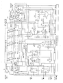
- Figure 1 shows a block diagram of the center frequency high resolution digital phase-locked loop in a clock recovery circuit implementation.
- the circuit consists of a center frequency high resolution digital phase correction circuit 1, a divide by K circuit 2, and a phase detector circuit 3.
- the center frequency correction circuit 1 generates a CLK OUT signal (f) which is divided by K (K ⁇ 1) in frequency to produce a RECEIVE CLK phase locked to the data transitions of a LIMITED DATA input.
- the clock reference input (CLK REF) to the phase correction circuit 1 is equal in frequency to the transmit clock frequency of the LIMITED DATA input. Advance or retard phase corrections are required to maintain phase lock to the LIMITED DATA signal transitions.
- the phase detector 3 generates an advance (ADV) or retard (RET) signal whenever the RECEIVE CLK is too late or too early, respectively, relative to the LIMITED DATA signal transitions.
- Each ADV or RET signal causes the phase lock loop to remove or introduce, respectively, a fixed delay (f) of CLK OUT and then output a clear correct signal (CLR CORRECT) which resets the phase detector ADV or RET output.
- the fixed delay (f) correction is in integer multiples of the propagation delay of two NAND gates, described hereinafter in greater detail.
- a RESET input to the phase control circuit 1 is used for initialization.
- Fig. 2 shows a block diagram of the center frequency high resolution digital phase correction circuit 1.
- the digital delay line 10 provides an incremental delay between 0 and 360 degrees of the CLK REF period.
- Shift register 11 selects the desired number of two NAND gate delays between 0 and n, where n is an integer greater than the CLK REF period divided by the worst case minimum two NAND gate delay.
- Clock correct control circuit 12 provides SHIFT CLK and left/right (L/-R) information to the shift register 11 based on the phase advance and phase retard input signals.
- L/-R left/right
- the 360 degree phase detect circuit 13 outputs a 360 DEG DETECT signal to the clock correct control circuit 12 when the DCLK output has been retarded by 360 degrees of the CLK REF period. This generates a shift register 11 initialization signal (SR INIT) which establishes zero delay in the digital delay line 10. Additional phase retard corrections can then occur. Thus, even though the digital delay line 10 only provides up to one CLK REF period of actual delay, it appears as an infinite delay line at the DCLK signal for phase retard requests.
- the 360 degree phase detector 13 uses the Qo through Qx taps of the shift register 11 to prevent false 360 degree phase detects for x-1 left shift clocks after SR INIT occurs.
- the shift overrun advance detector (SOA) 16 outputs an SOA signal to selector 15 and the SOA sequencer 17 when the DCLK signal is at zero delay and a phase advance occurs. This causes selector 15 to switch from the normally selected DCLK input to the BCLK REF input. While CLK OUT (f) provides a BCKL REF signal, the SOA sequencer overrides the ADV-RET inputs to clock correct control circuit 12 and executes a fast phase retard at the CLK REF frequency in search of 360 degree phase. Five signals from the SOA sequencer direct control of this fast phase retard: INH SR INIT, SR INIT C, FAST SHIFT, RET S, and RES SOA.
- the SOA sequencer commands several advance shifts to compensate for phase retard overshoot.
- RES SOA then occurs which inactivates shift overrun advance, switching selector 15 back to DCLK and allowing the ADV and RET signals to control the clock correct control circuit 12.
- Now additional advance corrections can occur with right shifts for one period of CLK REF where SOA again occurs and 360 degrees of phase delay is introduced.
- the combination of the 360 degree phase detect and SOA detect circuits 13 and 16 respectively allow the digital delay line 10 to look like an infinite delay line for both phase advance and phase retard phase corrections.
- the infinite delay line is not simulated perfectly during 0 to 360 degree and 360 to 0 degree phase transitions, the error is insignificant in most applications.
- the RESET input initializes the SOA sequencer 17 which outputs a BRESET signal to clock correct control circuit 12 and SOA detect circuit 16.
- Buffer 9 provides a buffered clock reference (BCLK REF) which is primarily required to drive the digital delay line 10.
- Buffer 14 buffers selector 15 output (UBCLK OUT) and provides drive capability for CLK OUT (f).
- FIG. 3 shows a detailed embodiment of the correction circuit 1.
- the digital delay line 10 is implemented using a serial chain of 1 of 2 data selectors (S0 - Sn).
- the selectors are non-inverting and can be implemented with NAND gates or with an equivalent such as AND-OR gates.
- a logic 0 or logic 1 on the bottom control lead selects the logic 0 or logic 1 input, respectively.
- the number of data selectors, n (not including S0), must be greater than the CLK REF period divided by the worst case minimum selector propagation delay.
- the Q outputs of shift register 11 control the selectors of the digital delay line 10.
- the 360 degree phase detector 13 consists of a 360 degree positive edge detector including flip flop 26, inverter 27, AND gate 28, and an inhibit circuit which prevents false 360 degree phase detects.
- the inhibit circuit consists of a 0 DEG inhibit circuit comprised of Exclusive NOR gate 29, AND gate 31 and flip flop 32 and a 180 DEG inhibit circuit comprised of gates 30, 31 and flip flop 32.
- the clock correct control circuit 12A is a shift clock and direction control circuit consisting of gates and flip flops 33 through 45, which provides an asynchronous phase advance and phase retard signal interface to the limited data phase detector 3 via the ADV, RET and CLR CORRECT signals.
- Figure 4 shows an embodiment of a phase detector 3 which will be described hereinafter.
- the shift overrun advance (SOA) detector 16 detects a shift right overrun which starts the SOA sequencer via the SOA signal.
- the SOA detector consists of gates and flip flop 20-25.
- the SOA sequencer 17 is a state machine which controls the clock correct control circuit 12A when searching for 360 degree delay.
- center frequency phase correction circuit 1 of Figure 3 The operation of the center frequency phase correction circuit 1 of Figure 3 will now be described for (a) the reset state, (b) retard corrections from 0 to 180 degrees, (c) retard corrections from 180 to 360 degrees, (d) advance correction at 0 degrees and (e) advance corrections from 360 to 0 degrees.
- Edge detector shift register 26 samples the DCLK signal at its D input on the falling edge of the BCLK REF signal. In the reset condition, the edge detector typically samples the digital delay line 10 output just before a falling edge.
- the shift register 26 thus typically contains all logic 1's, but due to worst case IC propagation delays all logic 0's or sporadic logic 0's and 1's could occur.
- the 360 DEG DET lead is also forced low via AND gate 28.
- SR INIT is inhibited from pulsing high even if the edge detector detects positive edges.
- the state of the 180 DEG -INH lead is high, but is a "don't care" state since the output of AND gate 31 is forced low by the 0 DEG -INH lead.
- the CLR CORRECT signal goes "high" on the third negative edge of BCLK REF to reset flip-flops 60 and 61 illustrated in the phase detector circuit of Figure 4A and restores the idle state of flip-flops 33, 34, 36 and 37 on the following three negative edges of BCLK REF.
- Each new phase retard request received causes the pair of "one's" in shift register 11 to shift left one position which adds an additional dT of delay to the CLK OUT signal.
- the pair of logic one's are shifted past Qx, the 0 DEG -INH line goes “high” since all logic "0's” are present on the inputs of NOR gate 29.
- the output of AND gate 31 then goes logic high assuming the 180 DEG -INH line is still high.After one CLK REF period, -INH goes high which enables the 360 degree detector 13.
- the Qx tap is chosen to inhibit a positive edge detect which otherwise might occur near zero degree phase and cause a shift register initialize (SR INIT) before 360 degree phase delay is reached. With worst case maximum selector propagation delays determine the Q output where 360 degree phase delay is selected. Qx is preferably selected to be about two taps before this tap. This ensures that the zero degree inhibit circuit will never mask valid 360 degree detects.
- CLK REF jitter or variations in selector gate delays can cause the foregoing condition to occur.
- EX-NOR gate 30 monitors the phase of BCLK REF and DCLK and charges capacitor C via resistor R to the average DC output voltage.
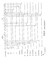
- Figure 5 shows the 180 degree inhibit circuit waveforms for the states 1, 0 or 1, 0, and 0 or 1 for the degrees of DCLK illustrated.
- the output of AND gate 31 and the -INH lead are logic low from about>90 degrees to ⁇ 270 degrees of phase delay. This assumes that the input switching threshold of AND gate 31 is at 2.5 volts. Input threshold variation will not affect the performance of the inhibit circuit, although the inhibit phase zone about 180 degrees will increase or decrease with a high or low threshold, respectively.
- the inhibit phase zone will never include the phase near 360 (or 0) degrees. This ensures that the 180 degree inhibit function will never mask valid 360 degree detects. Note that the 180 degree inhibit function can overlap with the 0 degree inhibit function and normally will do so with worst case maximum selector delays.
- the RC time constant is chose such that it is large enough to maintain a valid logic low when near 180 degrees of phase delay but small enough to not mask the 360 degree detect during fast retard with a worst case maximum average selector delay (minimum number of shifts to 360 degrees).
- the EX-NOR, R and C 180 degree inhibit circuit will always accurately mask the edge detects near 180 degrees whether 180 degrees is approached with phase advance or phase retard corrections. Even if no corrections occur and the delay line delay decreases from>180 degrees to ⁇ 180 degrees due to temperature variations, the positive edge detect will be masked. An all digital 180 degree inhibit circuit would not perform as well.
- edge detector shift register 26 outputs are 0 and the 360 degree detector is enabled.
- Q1 of shift register 26 goes to logic 1, 360 degree delay has been detected.
- the Q1 low to high transition forces SR INIT "high” via AND gate 28, OR gate 41 and AND gate 40.
- SR INIT returns low when flip-flop 32 samples the low output of AND gate 31.
- the correction circuit has now completed a 0 to 360 and back to 0 degree phase cycle.
- the correction circuit is now ready for additional phase retard requests.
- the Q0 output of shift register 26 is not used to allow metastable states to settle out during one period of CLK REF.
- the DCLK is asychronous relative to the sampling clock, BCLK REF, due to the incremental delays of the digital delay line 10.
- a metastable state could potentially delay the SR INIT pulse to occur after the BCLK REF returns high and cause an error condition in CLK OUT.
- the BCLK REF input at the logic "1" inputs of selectors S1 and S0 must be low before the Q1 or Q0 outputs go high as a result of SR INIT pulsing high.
- the inherent worst case minimum delays of gates, flip flop and register 26, 28, 41, 40 and 11 respectively typically provide an adequate total delay to compensate for maximum high-to-low transition time of BCLK REF, input threshold differences or layout variations.
- An advance request at 0 degrees requires that one CLK REF period delay be found to allow shift advance corrections to occur without overrunning the end of the shift register 11. This is done by performing a fast retard shift under the control of the shift overrun-advance (SOA) sequencer 17.
- SOA shift overrun-advance
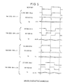
- FIG. 6 shows the timing as waveform diagrams for the SOA sequencer 17.
- the SOA sequencer 17 begins its control sequence when the SOA signal goes high.
- the basic operation of the SOA sequencer 17 is as follows:
- n + 11 CLK REF periods are required to complete the 360 degree phase retard search, where n is the number of selectors less one. In most applications this delay will not significantly affect clock correction accuracy, particularly when K of the divide by K circuit 2 of Figure 1 is large.
- Advance corrections from 360 to 0 degrees are performed essentially in the same manner as retard corrections except that the pair of logic one's in shift register 11 are shifted to the right instead of left. Each right shift removes a selector delay dT, which causes DCLK to advance relative to BCLK REF.
- the 0 to 180 degree inhibit circuits function the same as previously described for retard corrections.
- FIG. 4 A a phase detector 3 which attempts to center the negative edge of the RECEIVE CLK between incoming or limited data transitions is shown. It is to be understood that this is only an example of one type of phase detector which may be used with the present invention.
- Figure 4B shows the phase detector timing.
- Data flip-flops 52, 51 and 50 sample LIMITED DATA on the positive(sample 1), negative (center sample 2) and next positive (sample 1′) edges of the RECEIVE CLK, respectively as illustrated.
- the three samples are provided to a logic circuit comprised of gates 53 to 57 for evaluation and the result is output as a phase ADV or phase RET information signal upon the negative update edge of the RECEIVE CLK.
- Flip-flops 60 and 61 latch and hold this information via OR gates 58 and 59 until CLR CORRECT occurs.
- the RECEIVE CLK is corrected in increments of dT to maintain the negative edge of RECEIVE CLK approximately centered between limited data transitions.
- the shift register 11 of the center frequency phase-lock loop will shift the pair of logic "1's" left or right as required to phase-lock the RECEIVE CLK to the incoming LIMITED DATA.
- One preferred application of the center frequency phase-lock loop of the present invention shown in Figures 1 through 4 is in a Manchester data clock recovery circuit.
- This application uses the capability of the center frequency phase-lock loop to make small phase corrections to the output clock which is at the same frequency as the input CLK REF frequency.
- 6.528 M bps limited Manchester data may be provided to phase detector 3.
- a 13.056 Mhz crystal can be used to generate CLK REF with a worst case duty cycle of 40-60%.
- the typical selector delay is assumed as 4 nsec +/- 80% including process, temperature and voltage variations. The minimum and maximum selector delays are thus 0.8 nsec and 7.2 nsec, respectively.
- the RC time constant of the 180 degree inhibit circuit should be approximately 100 nsec.
- the accuracy of center sampling is dependent on the duty cycle of CLK REF. With a 60-40% duty cycle a +/- 10% sampling error can occur.
- Another preferred embodiment and application of the present invention is an ISDN U interface clock recovery at the line terminal (LT),and ideally requires that CLK OUT be phase locked between 0 and 360 degrees relative to the CLK REF input with no jitter. Occasional small phase steps are required to track the slowly changing phase of the limited data transitions from the network terminals due primarily to cable temperature variations.
- the present invention is well suited for this application.
- the IC technology employed provides that the maximum selector delay provides an acceptably small phase step ( ⁇ 1/1000 baud period). This ensures that the far end signal from the network terminal NT can be extracted from a signal which also includes the near end line terminal LT transmitted and echo signals with a minimum of error.
- LIMITED DATA as shown in Fig. 1 is actually zero crossing transition information from the four level 2B1Q signal derived via a zero crossing comparator.
- the phase detector 3 can be implemented with the circuit shown in Figure 4A.
- An averaging advance-retard counter circuit can be inserted between the phase detector 3 and center frequency phase-lock loop 1 to output only one correction request every few seconds. This provides the ability to track slow LIMITED DATA phase shifts due to cable temperature variations, while not following the high frequency jitter from the far end (NT).
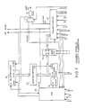
- FIG 7 shows a block diagram of a clock correct control circuit with gate delay compensation (12B).
- This clock correct control circuit can be used in place of the circuit 12 shown in Figure 3 to provide the additional features of gate delay compensation, bandwidth mode control, and shift register 11 all zero's recovery.
- Gate delay compensation reduces the worst case min-max dT correction range to 1:2 or better by using multiple dT corrections to build up the minimum dT correction.
- Bandwidth mode control allows control over the min-max correction range. Shift register 11 all zero's recovery prevents an all zero's lock-up state.
- Gate delay compensation of the phase-lock loop is required in many applications to provide a tighter tolerance correction. Since there is no high frequency reference to base each correction on, as in a conventional digital phase-lock loop, another approach must be taken. First the average selector propagation delay can be determined by counting the number of net retard shifts necessary to provide one CLK REF period delay. The average selector delay is then just the CLK REF period divided by this count. The desired minimum correction time is divided by this average selector delay to provide the number of dT corrections necessary to achieve this time. The minimum correction time must be greater than half the maximum dT correction. The worst case correction time accuracy covers a 1:2 min-max range regardless of the IC gate delay variation. The following equations summarize the above description and illustrate how the division operation can be simplified.
- INT(x/y) means the integer portion only of x/y after the division.
- the desired minimum correction time should be chosen to yield a 1/2**n result for MIN CORRECT TIME/CLK REF PERIOD in Eq. (3) where n is an integer.
- Simple binary division of AVG NET RET COUNT can then be performed by shifting left n times toward the most significant bit.
- the block diagram of Figure 7 illustrates a technique which uses binary division to compensate for gate delay variations.
- Average net retard counter 64 holds the average number of shift register 11 shift left-minus-right clocks required to go from 0 to 360 degree delay. This up/down counter is incremented or decremented one count each time SR INIT or RES SOA occurs via logic 65. Just before SR INIT or RES SOA occurs, the net retard counter 62 count A is compared to the average net retard counter count B by magnitude comparator 63. If A: B, then the average net retard count is incremented, otherwise it is decremented. The three most significant bits of the average net retard count (B6-B4) are provided to a mode control circuit 66. A binary divide-by-16 of B6-B0 is accomplished by using only B6-B4 which is equivalent to shifting left four bits.
- the mode control circuit maps B6-B4 to P2-P0 based on the C and D inputs.
- a programmable shift count generator 67 translates the P2-P0 input to the appropriate number of shift clocks for each phase advance or phase retard request.
- the binary count of P2-P0 plus 1 equals the number of shift clocks.
- Mode 0 is equivalent to no gate delay compensation since only one shift clock occurs for each correction.
- the clock correct control circuit of Fig. 7 can also be used in mode 0 for the Manchester data or ISDN LT clock recovery applications. Gate delay compensation is not required for either of these applications since even the worst case minimum phase step is still sufficient to track the data.
- shift register 11 must be in an undesired "all zero's" state. In this state A7 goes high and via logic 65 generates an SR INIT and resets the two counters 50 and 52. This action ensures recovery from all zero's in shift register 11.
- the circuit of Figure 7 is based on a range of .8 to 7.2 nsec selector delays and a minimum CLK REF frequency of 10 Mhz.
- the counter sizes, mode control operation and programmable shift count generator can be modified for other applications.
- a clock recovery application for an ISDN U interface at the network terminal (NT) illustrates the technique used for gate delay compensation and mode control. Requirements are similar to clock recovery at the line terminal (LT), except that a minimum correction of about 6 nsec is required to track the data under minimum transition and maximum jitter conditions. A maximum of 12.2 nsec results due to the worst case 1 to 2 range for gate delay compensation. This is still less than the maximum correction limit of about 1/1000 baud period (12.5 nsec). Substituting in the first fraction of Eq. (3):
- Table 1 shows the max and min average selector delay (dT), B6 B5 B4 and the no. of dT corrections for any average retard count from 0 to 127. This table is derived from Eq. (1) and the above.
- Mode 0 is equivalent to clock correct control circuit 12A in Figure 3 since only one shift clock is generated per retard request regardless of the average selector delay.
- the mode 0 correct time range is .769 to 7.2 nsec which is a 1:9.4 range.
- an alternative implementation of the center frequency high resolution digital phase locked loop reduces the 360 degree search time after SOA occurs.
- This consists of initializing shift register 11 only on power up. Retard corrections occur as described earlier except that shift register 11 R2 - Rn reset inputs are never pulsed during SR INIT, only S1 and S0.
- phase advance corrections a pair of logic "1's" are injected at the left end of shift register 11 at SRD based on the average net phase retard count.
- a pair of logic "1's" will be near 360 degrees of phase delay and an advance-retard search algorithm locates 360 degrees. In this approach it is difficult to recover from undesired shift register states.
- High speed fiber optic data and clock recovery circuits can also be implemented if high speed IC technology is used.
- a 500 Mbit/sec NRZ clock recovery circuit could be designed using a 500 Mhz CLK REF input to a gallium arsenide IC implementation of the invention.
- On-chip 100 psec selector delays would provide a resolution of 20 samples per bit.
- a conventional digital phase locked loop would require a very high 10 Ghz CLK REF input.
- the invention can be used in any application where a DPLL can be used without the requirement of a high frequency reference.
- a T1 1.544 Mhz clock recovery circuit can also be implemented using the invention with an appropriate phase detector and gate delay compensated correction time.
- the invention can also be used to implement a delay line with delay based on a clock reference.
- the delay is established by a programmable percentage of the average net retard count.
- IC process delay variations are compensated for upon initialization, and periodic calibration cycles compensate for temperature and voltage changes.
Landscapes
- Engineering & Computer Science (AREA)
- Computer Networks & Wireless Communication (AREA)
- Signal Processing (AREA)
- Stabilization Of Oscillater, Synchronisation, Frequency Synthesizers (AREA)
- Synchronisation In Digital Transmission Systems (AREA)
Applications Claiming Priority (2)
| Application Number | Priority Date | Filing Date | Title |
|---|---|---|---|
| US149459 | 1988-01-28 | ||
| US07/149,459 US4789996A (en) | 1988-01-28 | 1988-01-28 | Center frequency high resolution digital phase-lock loop circuit |
Publications (2)
| Publication Number | Publication Date |
|---|---|
| EP0326007A2 true EP0326007A2 (de) | 1989-08-02 |
| EP0326007A3 EP0326007A3 (de) | 1990-10-17 |
Family
ID=22530370
Family Applications (1)
| Application Number | Title | Priority Date | Filing Date |
|---|---|---|---|
| EP19890100813 Withdrawn EP0326007A3 (de) | 1988-01-28 | 1989-01-18 | Digitale phasenverriegelte Schleife mit hoher Auflösung für die zentrale Frequenz |
Country Status (3)
| Country | Link |
|---|---|
| US (1) | US4789996A (de) |
| EP (1) | EP0326007A3 (de) |
| NO (1) | NO890378L (de) |
Cited By (2)
| Publication number | Priority date | Publication date | Assignee | Title |
|---|---|---|---|---|
| AU614138B2 (en) * | 1988-06-03 | 1991-08-22 | Alcatel N.V. | A bit clock recovery method |
| CN101562450B (zh) * | 2008-04-16 | 2012-07-18 | 北京兆易创新科技有限公司 | 逐位逼近延迟锁相环电路以及调整时钟信号的方法 |
Families Citing this family (69)
| Publication number | Priority date | Publication date | Assignee | Title |
|---|---|---|---|---|
| US4964118A (en) * | 1988-10-24 | 1990-10-16 | Northern Telecom Limited | Apparatus and method for echo cancellation |
| US5087829A (en) * | 1988-12-07 | 1992-02-11 | Hitachi, Ltd. | High speed clock distribution system |
| GB8924202D0 (en) * | 1989-10-27 | 1989-12-13 | Ncr Co | Digital phase lock loop decoder |
| US5012494A (en) * | 1989-11-07 | 1991-04-30 | Hewlett-Packard Company | Method and apparatus for clock recovery and data retiming for random NRZ data |
| FR2658015B1 (fr) * | 1990-02-06 | 1994-07-29 | Bull Sa | Circuit verrouille en phase et multiplieur de frequence en resultant. |
| US5109394A (en) * | 1990-12-24 | 1992-04-28 | Ncr Corporation | All digital phase locked loop |
| US5295164A (en) * | 1991-12-23 | 1994-03-15 | Apple Computer, Inc. | Apparatus for providing a system clock locked to an external clock over a wide range of frequencies |
| US5451894A (en) * | 1993-02-24 | 1995-09-19 | Advanced Micro Devices, Inc. | Digital full range rotating phase shifter |
| JP3247190B2 (ja) * | 1993-04-13 | 2002-01-15 | 三菱電機株式会社 | 位相同期回路および集積回路装置 |
| US5552726A (en) * | 1993-05-05 | 1996-09-03 | Texas Instruments Incorporated | High resolution digital phase locked loop with automatic recovery logic |
| US5506874A (en) * | 1993-11-01 | 1996-04-09 | Texas Instruments Incorporated | Phase detector and method |
| JP2704103B2 (ja) * | 1993-11-09 | 1998-01-26 | 日本電気エンジニアリング株式会社 | 位相比較回路 |
| US5515403A (en) * | 1994-06-21 | 1996-05-07 | Dsc Communications Corporation | Apparatus and method for clock alignment and switching |
| US5828250A (en) * | 1994-09-06 | 1998-10-27 | Intel Corporation | Differential delay line clock generator with feedback phase control |
| JPH0884161A (ja) * | 1994-09-13 | 1996-03-26 | Fuji Electric Co Ltd | バイフェーズ符号を用いたシリアル通信装置用の受信検知回路装置 |
| US5796673A (en) * | 1994-10-06 | 1998-08-18 | Mosaid Technologies Incorporated | Delay locked loop implementation in a synchronous dynamic random access memory |
| JP3561792B2 (ja) * | 1995-09-06 | 2004-09-02 | 株式会社ルネサステクノロジ | クロック発生回路 |
| JP2926651B2 (ja) * | 1995-11-02 | 1999-07-28 | 株式会社鷹山 | マッチドフィルタ回路 |
| JPH09307407A (ja) * | 1996-05-09 | 1997-11-28 | Internatl Business Mach Corp <Ibm> | クロック発振器、クロック・ジェネレータ回路、クロック・パルスの発振方法 |
| US5991609A (en) * | 1996-12-26 | 1999-11-23 | Delco Electronics Corporation | Low cost digital automatic alignment method and apparatus |
| US5974105A (en) * | 1997-03-13 | 1999-10-26 | Industrial Technology Research Institute | High frequency all digital phase-locked loop |
| CA2204089C (en) * | 1997-04-30 | 2001-08-07 | Mosaid Technologies Incorporated | Digital delay locked loop |
| US6075832A (en) * | 1997-10-07 | 2000-06-13 | Intel Corporation | Method and apparatus for deskewing clock signals |
| US5990719A (en) * | 1997-10-07 | 1999-11-23 | Intel Corporation | Adaptive filtering scheme for sampling phase relations of clock networks |
| US6084933A (en) * | 1997-11-17 | 2000-07-04 | Advanced Micro Devices, Inc. | Chip operating conditions compensated clock generation |
| JP3048134B2 (ja) * | 1997-12-02 | 2000-06-05 | 日本電気株式会社 | クロック信号再生装置 |
| US6069506A (en) * | 1998-05-20 | 2000-05-30 | Micron Technology, Inc. | Method and apparatus for improving the performance of digital delay locked loop circuits |
| US6069507A (en) * | 1998-05-22 | 2000-05-30 | Silicon Magic Corporation | Circuit and method for reducing delay line length in delay-locked loops |
| KR100295052B1 (ko) * | 1998-09-02 | 2001-07-12 | 윤종용 | 전압제어지연라인의단위지연기들의수를가변시킬수있는제어부를구비하는지연동기루프및이에대한제어방법 |
| EP0987853A1 (de) | 1998-09-17 | 2000-03-22 | STMicroelectronics S.r.l. | Vollständig digitaler Phasenausrichter |
| KR100301048B1 (ko) | 1998-10-19 | 2001-09-06 | 윤종용 | 지연단의수가가변하는지연동기루프및이를구동하는방법 |
| US6415008B1 (en) | 1998-12-15 | 2002-07-02 | BéCHADE ROLAND ALBERT | Digital signal multiplier |
| JP3292169B2 (ja) * | 1999-02-24 | 2002-06-17 | 日本電気株式会社 | 半導体集積回路 |
| IT1311463B1 (it) * | 1999-12-31 | 2002-03-12 | Cit Alcatel | Metodo di recupero del segnale d'orologio in un sistema ditelecomunicazioni e relativo circuito. |
| US6774693B2 (en) * | 2000-01-18 | 2004-08-10 | Pmc-Sierra, Inc. | Digital delay line with synchronous control |
| US6273251B1 (en) * | 2000-04-24 | 2001-08-14 | Tim Rust | Travel protector for golf club heads |
| US6950487B2 (en) * | 2001-05-18 | 2005-09-27 | Micron Technology, Inc. | Phase splitter using digital delay locked loops |
| US7062004B1 (en) * | 2001-06-06 | 2006-06-13 | Silicon Image, Inc. | Method and apparatus for adaptive control of PLL loop bandwidth |
| DE10149585C2 (de) * | 2001-10-08 | 2003-11-20 | Infineon Technologies Ag | Integrierbare, steuerbare Verzögerungseinrichtung, Verwendung einer Verzögerungseinrichtung sowie Verfahren zum Betrieb einer Verzögerungseinrichtung |
| DE10149584B4 (de) | 2001-10-08 | 2007-11-22 | Infineon Technologies Ag | Verzögerungsregelkreis |
| US7221723B2 (en) * | 2001-11-27 | 2007-05-22 | Agilent Technologies, Inc. | Multi-phase sampling |
| US7546097B2 (en) * | 2002-03-06 | 2009-06-09 | Qualcomm Incorporated | Calibration techniques for frequency synthesizers |
| US20030194046A1 (en) * | 2002-04-11 | 2003-10-16 | Shirar Jerry Lester | Method for period counting using a tunable oscillator |
| US7098707B2 (en) * | 2004-03-09 | 2006-08-29 | Altera Corporation | Highly configurable PLL architecture for programmable logic |
| KR100713082B1 (ko) * | 2005-03-02 | 2007-05-02 | 주식회사 하이닉스반도체 | 클럭의 듀티 비율을 조정할 수 있는 지연 고정 루프 |
| GB2452748A (en) * | 2007-09-13 | 2009-03-18 | Cambridge Silicon Radio Ltd | Digital phase locked loop |
| US7893788B2 (en) * | 2008-02-19 | 2011-02-22 | Mediatek Inc. | Charge pump-based frequency modulator |
| JP4562787B2 (ja) * | 2008-07-30 | 2010-10-13 | ルネサスエレクトロニクス株式会社 | Pll回路 |
| JP4787870B2 (ja) * | 2008-10-02 | 2011-10-05 | 日本電波工業株式会社 | 周波数シンセサイザ |
| GB0821772D0 (en) * | 2008-11-28 | 2009-01-07 | Zarlink Semiconductor Inc | Soft reference switch for phase locked loop |
| CN101764608B (zh) * | 2008-12-25 | 2012-07-04 | 北京兆易创新科技有限公司 | 逐位逼近延迟锁相环电路及调整输入时钟信号的方法 |
| US7973612B2 (en) * | 2009-04-26 | 2011-07-05 | Qualcomm Incorporated | Supply-regulated phase-locked loop (PLL) and method of using |
| US8169265B2 (en) * | 2009-04-29 | 2012-05-01 | Mediatek Inc. | Phase lock loop circuits |
| US8368480B2 (en) * | 2009-06-24 | 2013-02-05 | Mediatek Inc. | Phase locked loop circuits and gain calibration methods thereof |
| CN101964658B (zh) * | 2009-07-23 | 2012-10-17 | 财团法人工业技术研究院 | 数字锁相回路与其数字相位频率侦测器 |
| CN102045061B (zh) * | 2009-10-16 | 2013-04-24 | 晨星软件研发(深圳)有限公司 | 锁相回路的回路频宽控制装置及回路频宽控制方法 |
| CN102045064B (zh) * | 2009-10-20 | 2013-03-13 | 群联电子股份有限公司 | 锁相回路及其压控振荡器 |
| CN102104376B (zh) * | 2009-12-16 | 2013-05-22 | 晨星软件研发(深圳)有限公司 | 相位产生装置及相位产生方法 |
| CN102158227B (zh) * | 2010-02-11 | 2013-04-17 | 奇景光电股份有限公司 | 非整数n型锁相回路 |
| JP4933635B2 (ja) * | 2010-02-19 | 2012-05-16 | 日本電波工業株式会社 | Pll回路 |
| CN102307047B (zh) * | 2010-06-01 | 2013-04-24 | 钰创科技股份有限公司 | 产生时钟脉冲数据回复信号相位锁住指标的电路及其方法 |
| CN101860361B (zh) * | 2010-06-03 | 2012-05-09 | 无锡中星微电子有限公司 | 一种延迟锁相环 |
| CN101951260B (zh) * | 2010-10-11 | 2012-10-17 | 上海电力学院 | 一种数字延迟锁相环电路 |
| US8400199B2 (en) * | 2010-11-26 | 2013-03-19 | Mediatek Inc. | Charge pump, phase frequency detector and charge pump methods |
| CN102185607B (zh) * | 2011-01-25 | 2013-11-06 | 上海华为技术有限公司 | 一种锁相环回路中相位差检测方法、装置及电路 |
| CN102130680B (zh) * | 2011-03-30 | 2013-05-08 | 苏州麦格芯微电子有限公司 | 一种温度补偿式晶体振荡器及其通讯方法 |
| CN102130679B (zh) * | 2011-04-12 | 2013-01-30 | 广州润芯信息技术有限公司 | 一种有源rc滤波器带宽校准方法 |
| CN102299709A (zh) * | 2011-04-27 | 2011-12-28 | 广州润芯信息技术有限公司 | 一种基于时间数字转换的高精度脉宽比较装置 |
| DE102012216326B4 (de) | 2012-09-13 | 2020-06-18 | TRUMPF Hüttinger GmbH + Co. KG | HF-Leistungsinvertersystem |
Family Cites Families (6)
| Publication number | Priority date | Publication date | Assignee | Title |
|---|---|---|---|---|
| US3509471A (en) * | 1966-11-16 | 1970-04-28 | Communications Satellite Corp | Digital phase lock loop for bit timing recovery |
| US4418318A (en) * | 1981-03-10 | 1983-11-29 | Frederick Electronics Corporation | Digital phase-locked loop circuit |
| US4385396A (en) * | 1981-06-05 | 1983-05-24 | Phillips Petroleum Company | NRZ Digital data recovery |
| US4574243A (en) * | 1984-01-03 | 1986-03-04 | Motorola, Inc. | Multiple frequency digital phase locked loop |
| JPS60204121A (ja) * | 1984-03-29 | 1985-10-15 | Fujitsu Ltd | 位相同期回路 |
| CA1297171C (en) * | 1986-04-01 | 1992-03-10 | Samuel Howard Gailbreath Jr. | Digital phase lock loop |
-
1988
- 1988-01-28 US US07/149,459 patent/US4789996A/en not_active Expired - Lifetime
-
1989
- 1989-01-18 EP EP19890100813 patent/EP0326007A3/de not_active Withdrawn
- 1989-01-30 NO NO89890378A patent/NO890378L/no unknown
Cited By (2)
| Publication number | Priority date | Publication date | Assignee | Title |
|---|---|---|---|---|
| AU614138B2 (en) * | 1988-06-03 | 1991-08-22 | Alcatel N.V. | A bit clock recovery method |
| CN101562450B (zh) * | 2008-04-16 | 2012-07-18 | 北京兆易创新科技有限公司 | 逐位逼近延迟锁相环电路以及调整时钟信号的方法 |
Also Published As
| Publication number | Publication date |
|---|---|
| NO890378L (no) | 1989-07-31 |
| EP0326007A3 (de) | 1990-10-17 |
| US4789996A (en) | 1988-12-06 |
| NO890378D0 (no) | 1989-01-30 |
Similar Documents
| Publication | Publication Date | Title |
|---|---|---|
| US4789996A (en) | Center frequency high resolution digital phase-lock loop circuit | |
| US4847870A (en) | High resolution digital phase-lock loop circuit | |
| US6584163B1 (en) | Shared data and clock recovery for packetized data | |
| US6760389B1 (en) | Data recovery for non-uniformly spaced edges | |
| US4821297A (en) | Digital phase locked loop clock recovery scheme | |
| US5412697A (en) | Delay line separator for data bus | |
| US4584695A (en) | Digital PLL decoder | |
| US4527277A (en) | Timing extraction circuit | |
| US7844021B2 (en) | Method and apparatus for clock skew calibration in a clock and data recovery system using multiphase sampling | |
| US7170964B2 (en) | Transition insensitive timing recovery method and apparatus | |
| EP0425302A2 (de) | Digitaler Phasenregelschleifendekoder | |
| US5491729A (en) | Digital phase-locked data recovery circuit | |
| KR100310190B1 (ko) | 비교기입력교환기술을갖는위상편차처리회로및로컬클럭신호발생방법과,이들을이용하는위상동기루프장치 | |
| CA1308448C (en) | Method of and circuit arrangement for recovering a bit clock from a received digital communication signal | |
| CA2037739C (en) | Frame synchronization dependent type bit synchronization extraction circuit | |
| US5644605A (en) | Jitter attenuator | |
| US6389090B2 (en) | Digital clock/data signal recovery method and apparatus | |
| US5751775A (en) | Transmission circuit of a line encoded signal on a telephone line | |
| EP0228021B1 (de) | Digitale phasenverriegelte Schleifenschaltungen | |
| US7450677B2 (en) | Clock and data recovery apparatus and method thereof | |
| US5717728A (en) | Data/clock recovery circuit | |
| WO2002014790A2 (en) | Cmi signal timing recovery | |
| EP1006660B1 (de) | Vorrichtung zur Wiedergewinnung und Identifizierung eines Taktsignals | |
| EP0732830A2 (de) | Schaltung zur Taktsignalgewinnung aus einem Hochgeschwindigkeitsdatenstrom | |
| US5058142A (en) | Clock extracting circuit in digital-line signal receiver |
Legal Events
| Date | Code | Title | Description |
|---|---|---|---|
| PUAI | Public reference made under article 153(3) epc to a published international application that has entered the european phase |
Free format text: ORIGINAL CODE: 0009012 |
|
| AK | Designated contracting states |
Kind code of ref document: A2 Designated state(s): AT BE CH DE ES FR GB GR IT LI NL SE |
|
| PUAL | Search report despatched |
Free format text: ORIGINAL CODE: 0009013 |
|
| AK | Designated contracting states |
Kind code of ref document: A3 Designated state(s): AT BE CH DE ES FR GB GR IT LI NL SE |
|
| 17P | Request for examination filed |
Effective date: 19901220 |
|
| 17Q | First examination report despatched |
Effective date: 19930205 |
|
| STAA | Information on the status of an ep patent application or granted ep patent |
Free format text: STATUS: THE APPLICATION IS DEEMED TO BE WITHDRAWN |
|
| 18D | Application deemed to be withdrawn |
Effective date: 19930616 |