EP0326465A1 - Schwebender Gate-EEPROM-Speicher mit einem Transistor zu Sourceleitungsauswahl - Google Patents
Schwebender Gate-EEPROM-Speicher mit einem Transistor zu Sourceleitungsauswahl Download PDFInfo
- Publication number
- EP0326465A1 EP0326465A1 EP89400169A EP89400169A EP0326465A1 EP 0326465 A1 EP0326465 A1 EP 0326465A1 EP 89400169 A EP89400169 A EP 89400169A EP 89400169 A EP89400169 A EP 89400169A EP 0326465 A1 EP0326465 A1 EP 0326465A1
- Authority
- EP
- European Patent Office
- Prior art keywords
- line
- floating gate
- transistor
- transistors
- floating
- Prior art date
- Legal status (The legal status is an assumption and is not a legal conclusion. Google has not performed a legal analysis and makes no representation as to the accuracy of the status listed.)
- Granted
Links
- 230000015654 memory Effects 0.000 title claims abstract description 46
- 239000004020 conductor Substances 0.000 claims description 9
- 239000004065 semiconductor Substances 0.000 claims description 8
- 101100049574 Human herpesvirus 6A (strain Uganda-1102) U5 gene Proteins 0.000 claims 1
- 101150064834 ssl1 gene Proteins 0.000 claims 1
- 101100371160 Saccharomyces cerevisiae (strain ATCC 204508 / S288c) TSL1 gene Proteins 0.000 abstract description 2
- 229910021420 polycrystalline silicon Inorganic materials 0.000 description 12
- 239000000758 substrate Substances 0.000 description 9
- 238000005530 etching Methods 0.000 description 7
- VYPSYNLAJGMNEJ-UHFFFAOYSA-N Silicium dioxide Chemical compound O=[Si]=O VYPSYNLAJGMNEJ-UHFFFAOYSA-N 0.000 description 3
- XUIMIQQOPSSXEZ-UHFFFAOYSA-N Silicon Chemical compound [Si] XUIMIQQOPSSXEZ-UHFFFAOYSA-N 0.000 description 3
- 229910052814 silicon oxide Inorganic materials 0.000 description 3
- 101000854908 Homo sapiens WD repeat-containing protein 11 Proteins 0.000 description 2
- 102100020705 WD repeat-containing protein 11 Human genes 0.000 description 2
- 240000008042 Zea mays Species 0.000 description 2
- 230000008021 deposition Effects 0.000 description 2
- 238000010586 diagram Methods 0.000 description 2
- 239000006185 dispersion Substances 0.000 description 2
- 230000000694 effects Effects 0.000 description 2
- 230000005684 electric field Effects 0.000 description 2
- 238000002513 implantation Methods 0.000 description 2
- 238000002347 injection Methods 0.000 description 2
- 239000007924 injection Substances 0.000 description 2
- 238000000034 method Methods 0.000 description 2
- 102100023927 Asparagine synthetase [glutamine-hydrolyzing] Human genes 0.000 description 1
- 101100380329 Homo sapiens ASNS gene Proteins 0.000 description 1
- OAICVXFJPJFONN-UHFFFAOYSA-N Phosphorus Chemical compound [P] OAICVXFJPJFONN-UHFFFAOYSA-N 0.000 description 1
- XAGFODPZIPBFFR-UHFFFAOYSA-N aluminium Chemical compound [Al] XAGFODPZIPBFFR-UHFFFAOYSA-N 0.000 description 1
- 229910052782 aluminium Inorganic materials 0.000 description 1
- 229910052785 arsenic Inorganic materials 0.000 description 1
- RQNWIZPPADIBDY-UHFFFAOYSA-N arsenic atom Chemical compound [As] RQNWIZPPADIBDY-UHFFFAOYSA-N 0.000 description 1
- 230000015572 biosynthetic process Effects 0.000 description 1
- 230000015556 catabolic process Effects 0.000 description 1
- 230000007547 defect Effects 0.000 description 1
- 230000002950 deficient Effects 0.000 description 1
- 238000009792 diffusion process Methods 0.000 description 1
- 238000005516 engineering process Methods 0.000 description 1
- 238000004519 manufacturing process Methods 0.000 description 1
- 239000000615 nonconductor Substances 0.000 description 1
- 229920005591 polysilicon Polymers 0.000 description 1
- 229910052710 silicon Inorganic materials 0.000 description 1
- 239000010703 silicon Substances 0.000 description 1
Images
Classifications
-
- H—ELECTRICITY
- H10—SEMICONDUCTOR DEVICES; ELECTRIC SOLID-STATE DEVICES NOT OTHERWISE PROVIDED FOR
- H10D—INORGANIC ELECTRIC SEMICONDUCTOR DEVICES
- H10D30/00—Field-effect transistors [FET]
- H10D30/60—Insulated-gate field-effect transistors [IGFET]
- H10D30/68—Floating-gate IGFETs
- H10D30/681—Floating-gate IGFETs having only two programming levels
- H10D30/684—Floating-gate IGFETs having only two programming levels programmed by hot carrier injection
- H10D30/685—Floating-gate IGFETs having only two programming levels programmed by hot carrier injection from the channel
-
- G—PHYSICS
- G11—INFORMATION STORAGE
- G11C—STATIC STORES
- G11C16/00—Erasable programmable read-only memories
- G11C16/02—Erasable programmable read-only memories electrically programmable
- G11C16/04—Erasable programmable read-only memories electrically programmable using variable threshold transistors, e.g. FAMOS
- G11C16/0408—Erasable programmable read-only memories electrically programmable using variable threshold transistors, e.g. FAMOS comprising cells containing floating gate transistors
- G11C16/0416—Erasable programmable read-only memories electrically programmable using variable threshold transistors, e.g. FAMOS comprising cells containing floating gate transistors comprising cells containing a single floating gate transistor and no select transistor, e.g. UV EPROM
-
- G—PHYSICS
- G11—INFORMATION STORAGE
- G11C—STATIC STORES
- G11C16/00—Erasable programmable read-only memories
- G11C16/02—Erasable programmable read-only memories electrically programmable
- G11C16/04—Erasable programmable read-only memories electrically programmable using variable threshold transistors, e.g. FAMOS
- G11C16/0408—Erasable programmable read-only memories electrically programmable using variable threshold transistors, e.g. FAMOS comprising cells containing floating gate transistors
- G11C16/0425—Erasable programmable read-only memories electrically programmable using variable threshold transistors, e.g. FAMOS comprising cells containing floating gate transistors comprising cells containing a merged floating gate and select transistor
-
- H—ELECTRICITY
- H10—SEMICONDUCTOR DEVICES; ELECTRIC SOLID-STATE DEVICES NOT OTHERWISE PROVIDED FOR
- H10B—ELECTRONIC MEMORY DEVICES
- H10B41/00—Electrically erasable-and-programmable ROM [EEPROM] devices comprising floating gates
-
- H—ELECTRICITY
- H10—SEMICONDUCTOR DEVICES; ELECTRIC SOLID-STATE DEVICES NOT OTHERWISE PROVIDED FOR
- H10B—ELECTRONIC MEMORY DEVICES
- H10B69/00—Erasable-and-programmable ROM [EPROM] devices not provided for in groups H10B41/00 - H10B63/00, e.g. ultraviolet erasable-and-programmable ROM [UVEPROM] devices
Definitions
- the invention relates to integrated circuit memories, and more precisely memories of the EEPROM type, that is to say non-volatile memories, programmable and electrically erasable.
- the control gate of this transistor When a programming operation for a transistor of a column of memory points is going to be carried out, the control gate of this transistor will be brought to a positive potential with respect to the source, as well as its drain. The gate of the other transistors will remain at zero potential so that these transistors are not conductive during the programming operation. But if some of them have too high a leakage current, due for example to positive charges on their floating gate, the drain potential of the transistor that trying to program will drop and deteriorate the efficiency of electron injection in the floating gate so that there is a risk of bad programming of this memory point.
- the article cited above proposes to put in series with each floating gate transistor a transistor controlled by the control gate of the floating gate transistor.
- This series transistor is not a floating gate transistor; its leakage current can be kept at a low value by appropriately doping its channel (normally enriched transistor); this transistor therefore prevents the leakage current of the floating gate transistor with which it is in series from circulating, even if the floating gate is positively charged as a result of overly high erasure.
- this additional transistor simply consist of a portion of the control gate of the floating gate transistor, covering a part of the transistor channel not covered by the floating gate.
- the control gate is extended beyond the floating gate above a channel region in series with the channel of the floating gate transistor.
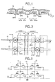
- Figures 1, 2, and 3 show a memory structure that can be imagined from the memory point proposed in the prior art.
- Figure 1 is a sectional view of two adjacent memory points of the same column (section along line A-A of Figure 2);
- FIG. 2 represents a top view of a portion of the memory, showing four memory points at the intersection of two adjacent lines and two adjacent columns;
- FIG. 3 represents an equivalent electrical diagram of the structure of FIGS. 1 and 2.
- the memory is produced from a semiconductor substrate 10 which is for example of the P type.
- Each memory point comprises a floating gate transistor and a selection transistor.
- the floating gate transistors are designated respectively by TGF11 at the intersection of row 1 and column 1, TGF12 at the intersection of row 1 and column 2, TGF21 at the intersection of row 2 and column 1, and TGF22 at the intersection of line 2 and column 2.
- the selection transistors are designated respectively by TS11, TS12, TS21, TS22 the indices having the same meaning as for the floating gate transistors.
- each floating gate transistor is a N type diffused region connected to a column conductor, C1 for column 1, C2 for column 2.
- Floating gates are rectangles of polycrystalline silicon overhanging a portion of P-type semiconductor substrate adjacent to the drain regions.
- the control gates of the floating gate transistors are formed by polycrystalline silicon strips L1 for line 1, L2 for line 2, extending perpendicularly to column conductors C1, C2. These bands overhang both the floating gates of the transistors of the corresponding line, and as such they constitute the control gates of the transistors with floating gate; but they also extend above a part of P-type substrate not covered by the floating gate and adjacent to the part covered by the floating gate, and as such they also constitute control gates for the selection transistors.
- the semiconductor zone located between the two bands L1 and L2 is an N-type doped diffused line SC, constituting the source of the selection transistors attached to the two lines L1 and L2.
- the sources of the selection transistors are in fact intended to be brought to a potential which is the same for all the transistors of the memory plane (even if this potential varies over time) and it is very frequent in conventional EPROM memory plans or EEPROM thus have two adjacent transistor lines with an N-type diffused line between these transistor lines, to serve as a source line for two rows of transistor at a time. This avoids having to provide one source line per line of transistors and this saves space.
- each transistor shares its drain on the other side with another adjacent transistor in the same column.
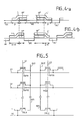
- Figure 4 (4a, 4b, 4c) is intended to illustrate the problem posed by the presence of two superimposed grids of different widths.
- the manufacturing process begins with the formation of active regions delimited by silicon oxide thick, not shown, surrounding the drain regions and the source lines and separating the adjacent transistors from neighboring columns.
- the edge of the control grids L and L ′ (on the side of the source SC or SC ′ Respectively) is at a desired distance D from the edge of the floating gate (GF or GF ′ respectively) on the source side as well.
- the edge of the floating gate GF or GF ′ is defined by an etching operation of the first level of polycrystalline silicon, before deposition of the second level of polycrystalline silicon. This edge therefore constitutes a reference for the engraving of the second level.
- the other edge of the floating grid on the side of the DR drain
- FIG. 4b an unfavorable case has been represented in which the mask for aligning the control grids (that is to say word lines L and L ′) is slightly shifted to the left with respect to the pattern of GF and GF ′ floating grids already engraved.
- the left edge of the word line L is at a distance D + d (instead of D) from the left edge of the floating grid GF, and conversely that the edge right of the word line L ′ is at a distance D - d from the right edge of the floating grid GF ′.
- the two adjacent memory points in FIG. 4, which theoretically have mirror symmetry with respect to the drain DR which they share, are no longer symmetrical in FIG. 4b.
- One has a channel length too short for the floating gate transistor and too long for the control transistor; the other, on the contrary, has a channel length that is too long for the floating gate transistor and a channel length that is too short for the control transistor.
- each memory point be constituted by a floating gate transistor, the floating gate extending from the drain region to the source region (consequently without selection transistor constituted by a extension of the control gate above a substrate region not covered by the floating gate), a single selection transistor for a whole line of transistors being provided between a source line corresponding to this line of transistors and a conductor of control of all sources of floating gate transistors of the memory plane, this selection transistor having a control gate connected to the comm grids ande of floating gate transistors of the same line.
- the structure proposed by the invention for an erasable non-volatile memory and electrically reprogrammable is as follows: the memory is organized into rows and columns of memory points, each memory point comprising a floating gate transistor having a source, a drain, a floating gate, and a control gate; the drains of the transistors of the same column are connected to the same bit line and the control gates of the transistors of the same line are connected to the same word line; the sources of the transistors of the same line are connected to the drain of a selection transistor common to the whole line, this transistor having its gate connected to the word line of the transistors of the line considered and its source connected to a common conductor to all lines of transistors. This common conductor will generally be connected to ground.
- the sources of the transistors connected to the same word line are constituted by a semiconductor line diffused in the substrate, this diffused line also constituting a drain region for the selection transistor.
- this diffused line also constituting a drain region for the selection transistor.
- the control gates of the floating gate transistors of a line are formed by a conductive strip constituting a word line, then provision is made for this strip also to constitute the control gate of the selection transistor.
- the selection transistor is placed in principle at the end of the line. We can also provide one at each end of the line.
- provision may be made for the diffused source lines to be more doped than the drains of the floating gate transistors.
- each line of transistors has its source line, SC1 for line 1 and SC2 for line 2; the source lines of the different transistor lines are not connected to each other and are not directly brought to ground potential as is the case in the prior art.
- a source line is connected to the drain of a respective selection transistor corresponding to this source line; the gate of this transistor is connected to the control gates of the floating gate transistors of the same line, and the source of this selection transistor is connected to a conductor SC which brings the potential necessary to the sources of the floating gate transistors in phase of programming (in principle the potential of the SC conductor is that of the ground).
- the source line selection transistor is designated by TSL1 for line 1 and TSL2 for line 2. Only the source line corresponding to a designated line of memory points will actually be brought to ground potential; the designation of the line of points is in fact done by applying to the word line (L1 or L2) a potential tending to make the floating gate transistors conductive, and the mounting is such that this potential also makes the transistor conductive source line selection. The other source line selection transistors remain blocked and prevent the leakage currents from the transistors of the non-selected lines towards the source.
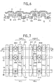
- Figures 6 and 7 show, respectively in section (along line B-B of Figure 7) and in top view, a possible practical arrangement for the invention.
- the source lines SC1 and SC2 are N + type diffused semiconductor lines (for N-channel transistors), extending parallel to the word lines L1 and L2; they are delimited on the one hand by thick silicon oxide regions 14 which separate them from the source of the adjacent line, and on the other hand by the edges of the gates of the floating gate transistors. floating gate transistors.
- the drains (DR11 to DR22) are constituted as in the prior art by diffused rectangles of type N + delimited on the one hand by the thick oxide and on the other hand by the grids of the transistors with floating gate.
- Floating gates are rectangles of polycrystalline silicon (first level of polycrystalline silicon) isolated from the semiconductor substrate and overhanging the space between a region drain of a transistor and the corresponding source line.
- the word lines (L1, L2) are bands of polycrystalline silicon (second level of polycrystalline silicon) which directly constitute the control gates of the floating gate transistors; the word lines are separated from the floating grids by thin silicon oxide; the width of the bands constituting the word lines is exactly the same as the width of the floating grids and this width is preferably defined by a single etching operation (the length having been defined by a previous etching of the first level of silicon since the grids floating points do not extend in bands but are located at each transistor site).
- the source and drain regions are all defined by implantation and diffusion, after etching of the two grids, so that not only the grids have their edges self-aligned with each other, but the source and drain regions are also self-aligned with respect to these grids (and relative to thick oxide areas).
- the bit lines C1, C2 are preferably metallic conductors (for example made of aluminum) extending in strips transversely to the word lines and coming to contact punctually, through an insulating layer which separates them from the polycrystalline silicon and from the semiconductor substrate, the drain regions of the transistors corresponding to this word line.
- the source lines SC1, SC2 will be more doped than the drain regions (doping by double phosphor + Arsenic implantation) so as to support the erasing voltage (from 16 to 20 V) without diode breakdown.
- the word line is only separated from the substrate by a thin layer of oxide so that it can serve to control the conduction of the selection transistor.
- the selection transistor is a normally enriched transistor, that is to say a non-conductor in the presence of a zero gate-source voltage.
- the channel width of the selection transistors is large enough not to introduce an excessive voltage drop during programming in particular.
- this selection transistor is formed at the same time as the floating gate transistors and its source and its drain are self-aligned with respect to the word line L1 and are further delimited by thick oxide which separates them from the other regions of source and drain of the structure.
- each transistor shares its drain with an adjacent transistor of the same column, and this is true for the floating gate transistors as for the selection transistors.
Landscapes
- Engineering & Computer Science (AREA)
- Microelectronics & Electronic Packaging (AREA)
- Non-Volatile Memory (AREA)
- Semiconductor Memories (AREA)
- Read Only Memory (AREA)
Applications Claiming Priority (2)
| Application Number | Priority Date | Filing Date | Title |
|---|---|---|---|
| FR8800859A FR2626401B1 (fr) | 1988-01-26 | 1988-01-26 | Memoire eeprom a grille flottante avec transistor de selection de ligne de source |
| FR8800859 | 1988-01-26 |
Publications (2)
| Publication Number | Publication Date |
|---|---|
| EP0326465A1 true EP0326465A1 (de) | 1989-08-02 |
| EP0326465B1 EP0326465B1 (de) | 1993-03-31 |
Family
ID=9362641
Family Applications (1)
| Application Number | Title | Priority Date | Filing Date |
|---|---|---|---|
| EP89400169A Expired - Lifetime EP0326465B1 (de) | 1988-01-26 | 1989-01-20 | Schwebender Gate-EEPROM-Speicher mit einem Transistor zu Sourceleitungsauswahl |
Country Status (5)
| Country | Link |
|---|---|
| EP (1) | EP0326465B1 (de) |
| JP (1) | JP2613859B2 (de) |
| KR (1) | KR890012322A (de) |
| DE (1) | DE68905622T2 (de) |
| FR (1) | FR2626401B1 (de) |
Cited By (12)
| Publication number | Priority date | Publication date | Assignee | Title |
|---|---|---|---|---|
| EP0434121A1 (de) * | 1989-12-22 | 1991-06-26 | STMicroelectronics S.r.l. | Nichtflüchtige EPROM-Speicherzelle mit geteiltem Gate und selbstausrichtendes Feldisolierungsverfahren zur Herstellung |
| EP0411347A3 (en) * | 1989-08-01 | 1992-03-11 | Sgs-Thomson Microelectronics S.R.L. | Eeprom memory cell with improved protection against errors due to cell breakdown |
| EP0461764A3 (en) * | 1990-06-13 | 1992-06-03 | Waferscale Integration, Inc. | Eprom virtual ground array |
| EP0486249A3 (en) * | 1990-11-13 | 1993-05-19 | Waferscale Integration, Inc. | Eprom array |
| US5327378A (en) * | 1992-03-04 | 1994-07-05 | Waferscale Integration, Inc. | Easily manufacturable compact EPROM |
| EP0618586A1 (de) * | 1993-03-31 | 1994-10-05 | Sony Corporation | Nichtflüchtige Speicheranordnung |
| EP0637035A1 (de) * | 1993-07-29 | 1995-02-01 | STMicroelectronics S.r.l. | Schaltungsstruktur für Speichermatrix und entsprechende Herstellungsverfahren |
| WO1999013513A1 (en) * | 1997-09-09 | 1999-03-18 | Interuniversitair Micro-Elektronica Centrum | Non-volatile memory cell |
| WO2002037502A3 (en) * | 2000-10-30 | 2003-09-25 | Virtual Silicon Technology Inc | Common source eeprom and flash memory |
| FR2843648A1 (fr) * | 2002-08-14 | 2004-02-20 | Samsung Electronics Co Ltd | Dispositif a memoire flash ayant une ligne de source stable independamment du couplage de la ligne de bits et d'un effet de charge |
| SG108920A1 (en) * | 1999-07-14 | 2005-02-28 | Hitachi Ltd | Semiconductor integrated circuit device, production and operation method thereof |
| US6901006B1 (en) | 1999-07-14 | 2005-05-31 | Hitachi, Ltd. | Semiconductor integrated circuit device including first, second and third gates |
Families Citing this family (6)
| Publication number | Priority date | Publication date | Assignee | Title |
|---|---|---|---|---|
| JP2694205B2 (ja) * | 1988-07-11 | 1997-12-24 | 株式会社日立製作所 | 不揮発性半導体記憶装置 |
| US5138575A (en) * | 1988-12-19 | 1992-08-11 | Fujitsu Limited | Electricaly erasable and programmable read only memory with a discharge device |
| JPH03235295A (ja) * | 1990-02-08 | 1991-10-21 | Mitsubishi Electric Corp | 不揮発性記憶装置 |
| JPH04226032A (ja) * | 1990-04-20 | 1992-08-14 | Toshiba Corp | 半導体装置およびその製造方法 |
| JP2827607B2 (ja) * | 1991-09-12 | 1998-11-25 | 三菱電機株式会社 | 半導体記憶装置 |
| JP2751821B2 (ja) * | 1994-02-16 | 1998-05-18 | 日本電気株式会社 | 不揮発性半導体記憶装置 |
Citations (2)
| Publication number | Priority date | Publication date | Assignee | Title |
|---|---|---|---|---|
| US4087795A (en) * | 1974-09-20 | 1978-05-02 | Siemens Aktiengesellschaft | Memory field effect storage device |
| FR2468972A1 (fr) * | 1979-10-29 | 1981-05-08 | Texas Instruments Inc | Matrice de memoire permanente programmable ou non, a masse virtuelle |
Family Cites Families (1)
| Publication number | Priority date | Publication date | Assignee | Title |
|---|---|---|---|---|
| JPS5730373A (en) * | 1980-07-30 | 1982-02-18 | Fujitsu Ltd | Semiconductor nonvolatile memory |
-
1988
- 1988-01-26 FR FR8800859A patent/FR2626401B1/fr not_active Expired - Lifetime
-
1989
- 1989-01-20 EP EP89400169A patent/EP0326465B1/de not_active Expired - Lifetime
- 1989-01-20 DE DE8989400169T patent/DE68905622T2/de not_active Expired - Fee Related
- 1989-01-25 JP JP1606689A patent/JP2613859B2/ja not_active Expired - Lifetime
- 1989-01-26 KR KR1019890000850A patent/KR890012322A/ko not_active Withdrawn
Patent Citations (2)
| Publication number | Priority date | Publication date | Assignee | Title |
|---|---|---|---|---|
| US4087795A (en) * | 1974-09-20 | 1978-05-02 | Siemens Aktiengesellschaft | Memory field effect storage device |
| FR2468972A1 (fr) * | 1979-10-29 | 1981-05-08 | Texas Instruments Inc | Matrice de memoire permanente programmable ou non, a masse virtuelle |
Non-Patent Citations (2)
| Title |
|---|
| PATENT ABSTRACTS OF JAPAN, vol. 6, no. 95 (E-110)[973], 3 juin 1982, page 165 E 110; & JP-A-57 30 373 (FUJITSU K.K.) 18-02-1982 * |
| SIEMENS FORSCHUNGS- UND ENTWICKLUNGSBERICHTE RESEARCH AND DEVELOPMENT REPORTS, vol. 4, no. 6, 1975, pages 345-351, Springer Verlag; B. RÖSSLER et al.: "Erasable and electrically reprogrammable read-only memory using the N-channel SIMOS one-transistor cell" * |
Cited By (20)
| Publication number | Priority date | Publication date | Assignee | Title |
|---|---|---|---|---|
| EP0411347A3 (en) * | 1989-08-01 | 1992-03-11 | Sgs-Thomson Microelectronics S.R.L. | Eeprom memory cell with improved protection against errors due to cell breakdown |
| EP0434121A1 (de) * | 1989-12-22 | 1991-06-26 | STMicroelectronics S.r.l. | Nichtflüchtige EPROM-Speicherzelle mit geteiltem Gate und selbstausrichtendes Feldisolierungsverfahren zur Herstellung |
| US5241499A (en) * | 1989-12-22 | 1993-08-31 | Sgs-Thomson Microelectronics S.R.L. | Non-volatile split gate eprom memory cell and self-aligned field insulation process for obtaining the above cell |
| US5330938A (en) * | 1989-12-22 | 1994-07-19 | Sgs-Thomson Microelectronics S.R.L. | Method of making non-volatile split gate EPROM memory cell and self-aligned field insulation |
| EP0461764A3 (en) * | 1990-06-13 | 1992-06-03 | Waferscale Integration, Inc. | Eprom virtual ground array |
| US5204835A (en) * | 1990-06-13 | 1993-04-20 | Waferscale Integration Inc. | Eprom virtual ground array |
| EP0486249A3 (en) * | 1990-11-13 | 1993-05-19 | Waferscale Integration, Inc. | Eprom array |
| US5862076A (en) * | 1990-11-13 | 1999-01-19 | Waferscale Integration, Inc. | Fast EPROM array |
| US5327378A (en) * | 1992-03-04 | 1994-07-05 | Waferscale Integration, Inc. | Easily manufacturable compact EPROM |
| EP0618586A1 (de) * | 1993-03-31 | 1994-10-05 | Sony Corporation | Nichtflüchtige Speicheranordnung |
| US5597750A (en) * | 1993-07-29 | 1997-01-28 | Sgs-Thomson Microelectronics S.R.L. | Method of manufacturing a matrix of memory cells having control gates |
| US5677871A (en) * | 1993-07-29 | 1997-10-14 | Sgs-Thomson Microelectronics S.R.L. | Circuit structure for a memory matrix and corresponding manufacturing method |
| EP0637035A1 (de) * | 1993-07-29 | 1995-02-01 | STMicroelectronics S.r.l. | Schaltungsstruktur für Speichermatrix und entsprechende Herstellungsverfahren |
| WO1999013513A1 (en) * | 1997-09-09 | 1999-03-18 | Interuniversitair Micro-Elektronica Centrum | Non-volatile memory cell |
| US6486509B1 (en) | 1997-09-09 | 2002-11-26 | Imec Vzw | Non-volatile memory cell |
| SG108920A1 (en) * | 1999-07-14 | 2005-02-28 | Hitachi Ltd | Semiconductor integrated circuit device, production and operation method thereof |
| US6901006B1 (en) | 1999-07-14 | 2005-05-31 | Hitachi, Ltd. | Semiconductor integrated circuit device including first, second and third gates |
| WO2002037502A3 (en) * | 2000-10-30 | 2003-09-25 | Virtual Silicon Technology Inc | Common source eeprom and flash memory |
| USRE40976E1 (en) | 2000-10-30 | 2009-11-17 | Albert Bergemont | Common source EEPROM and flash memory |
| FR2843648A1 (fr) * | 2002-08-14 | 2004-02-20 | Samsung Electronics Co Ltd | Dispositif a memoire flash ayant une ligne de source stable independamment du couplage de la ligne de bits et d'un effet de charge |
Also Published As
| Publication number | Publication date |
|---|---|
| JPH025470A (ja) | 1990-01-10 |
| FR2626401B1 (fr) | 1990-05-18 |
| KR890012322A (ko) | 1989-08-25 |
| DE68905622D1 (de) | 1993-05-06 |
| DE68905622T2 (de) | 1993-07-08 |
| FR2626401A1 (fr) | 1989-07-28 |
| JP2613859B2 (ja) | 1997-05-28 |
| EP0326465B1 (de) | 1993-03-31 |
Similar Documents
| Publication | Publication Date | Title |
|---|---|---|
| EP0326465B1 (de) | Schwebender Gate-EEPROM-Speicher mit einem Transistor zu Sourceleitungsauswahl | |
| US4649520A (en) | Single layer polycrystalline floating gate | |
| JP3606596B2 (ja) | 集積デバイスの製造方法 | |
| US6436766B1 (en) | Process for fabricating high density memory cells using a polysilicon hard mask | |
| EP0648375B1 (de) | Flash-eeprom-speicher mit drei gateelektroden und sein herstellungsverfahren. | |
| JPH06112501A (ja) | 不揮発性半導体メモリ装置及びその製造方法 | |
| JPH07221209A (ja) | プログラム用の高い熱い電子注入効率のための浮遊ゲートとドレイン間にギャップを有するフラッシュeepromセル | |
| JPH05218356A (ja) | 埋込形ビットラインソース側注入式フラッシュメモリセル及びその製造方法 | |
| JPH09504410A (ja) | Eprom又はフラッシュメモリアレイにおける酸化膜の薄膜化の制御方法 | |
| US20020045320A1 (en) | Nonvolatile memory device and method for manufacturing the same | |
| FR2987700A1 (fr) | Memoire non volatile comprenant des mini caissons a potentiel flottant | |
| EP0675547B1 (de) | Elektrisch programmierbare Speicherzelle | |
| WO1996027904A1 (en) | Eeprom on insulator | |
| US6399446B1 (en) | Process for fabricating high density memory cells using a metallic hard mask | |
| EP0573168A1 (de) | AMG-EPROM mit schneller Zugriffszeit | |
| EP0282520B1 (de) | Nichtflüchtiger speicher mit isoliertem gate ohne dickes oxid | |
| US5904524A (en) | Method of making scalable tunnel oxide window with no isolation edges | |
| EP0896370B1 (de) | Schwebegatterspeicherelement auf SOI und entsprechendes Herstellungsverfahren | |
| FR2723259A1 (fr) | Thyristor a commande par mos ayant des caracteristiques de saturation de courant | |
| US6136647A (en) | Method of forming interpoly dielectric and gate oxide in a memory cell | |
| FR2511801A1 (fr) | Memoire d'informations et son procede de fabrication | |
| US5057446A (en) | Method of making an EEPROM with improved capacitive coupling between control gate and floating gate | |
| FR2491678A1 (fr) | Procede de fabrication d'un transistor a effet de champ et dispositif obtenu selon ce procede | |
| EP0313427B1 (de) | Speicher in einer integrierten Schaltung | |
| US5838616A (en) | Gate edge aligned EEPROM transistor |
Legal Events
| Date | Code | Title | Description |
|---|---|---|---|
| PUAI | Public reference made under article 153(3) epc to a published international application that has entered the european phase |
Free format text: ORIGINAL CODE: 0009012 |
|
| AK | Designated contracting states |
Kind code of ref document: A1 Designated state(s): DE ES GB IT NL |
|
| 17P | Request for examination filed |
Effective date: 19890918 |
|
| 17Q | First examination report despatched |
Effective date: 19920518 |
|
| ITF | It: translation for a ep patent filed | ||
| GRAA | (expected) grant |
Free format text: ORIGINAL CODE: 0009210 |
|
| AK | Designated contracting states |
Kind code of ref document: B1 Designated state(s): DE ES GB IT NL |
|
| PG25 | Lapsed in a contracting state [announced via postgrant information from national office to epo] |
Ref country code: NL Effective date: 19930331 Ref country code: ES Free format text: THE PATENT HAS BEEN ANNULLED BY A DECISION OF A NATIONAL AUTHORITY Effective date: 19930331 |
|
| REF | Corresponds to: |
Ref document number: 68905622 Country of ref document: DE Date of ref document: 19930506 |
|
| GBT | Gb: translation of ep patent filed (gb section 77(6)(a)/1977) |
Effective date: 19930519 |
|
| NLV1 | Nl: lapsed or annulled due to failure to fulfill the requirements of art. 29p and 29m of the patents act | ||
| PLBE | No opposition filed within time limit |
Free format text: ORIGINAL CODE: 0009261 |
|
| STAA | Information on the status of an ep patent application or granted ep patent |
Free format text: STATUS: NO OPPOSITION FILED WITHIN TIME LIMIT |
|
| 26N | No opposition filed | ||
| PGFP | Annual fee paid to national office [announced via postgrant information from national office to epo] |
Ref country code: DE Payment date: 20010115 Year of fee payment: 13 |
|
| REG | Reference to a national code |
Ref country code: GB Ref legal event code: IF02 |
|
| PG25 | Lapsed in a contracting state [announced via postgrant information from national office to epo] |
Ref country code: DE Free format text: LAPSE BECAUSE OF NON-PAYMENT OF DUE FEES Effective date: 20020801 |
|
| PGFP | Annual fee paid to national office [announced via postgrant information from national office to epo] |
Ref country code: GB Payment date: 20030122 Year of fee payment: 15 |
|
| PG25 | Lapsed in a contracting state [announced via postgrant information from national office to epo] |
Ref country code: GB Free format text: LAPSE BECAUSE OF NON-PAYMENT OF DUE FEES Effective date: 20040120 |
|
| GBPC | Gb: european patent ceased through non-payment of renewal fee |
Effective date: 20040120 |
|
| PG25 | Lapsed in a contracting state [announced via postgrant information from national office to epo] |
Ref country code: IT Free format text: LAPSE BECAUSE OF NON-PAYMENT OF DUE FEES;WARNING: LAPSES OF ITALIAN PATENTS WITH EFFECTIVE DATE BEFORE 2007 MAY HAVE OCCURRED AT ANY TIME BEFORE 2007. THE CORRECT EFFECTIVE DATE MAY BE DIFFERENT FROM THE ONE RECORDED. Effective date: 20050120 |