EP0326952A2 - Circuit d'interface bipolaire-CMOS - Google Patents
Circuit d'interface bipolaire-CMOS Download PDFInfo
- Publication number
- EP0326952A2 EP0326952A2 EP89101383A EP89101383A EP0326952A2 EP 0326952 A2 EP0326952 A2 EP 0326952A2 EP 89101383 A EP89101383 A EP 89101383A EP 89101383 A EP89101383 A EP 89101383A EP 0326952 A2 EP0326952 A2 EP 0326952A2
- Authority
- EP
- European Patent Office
- Prior art keywords
- translator
- circuit
- transistor
- translator circuit
- simulated
- Prior art date
- Legal status (The legal status is an assumption and is not a legal conclusion. Google has not performed a legal analysis and makes no representation as to the accuracy of the status listed.)
- Ceased
Links
Images

Classifications
-
- H—ELECTRICITY
- H03—ELECTRONIC CIRCUITRY
- H03K—PULSE TECHNIQUE
- H03K19/00—Logic circuits, i.e. having at least two inputs acting on one output; Inverting circuits
- H03K19/02—Logic circuits, i.e. having at least two inputs acting on one output; Inverting circuits using specified components
- H03K19/08—Logic circuits, i.e. having at least two inputs acting on one output; Inverting circuits using specified components using semiconductor devices
- H03K19/094—Logic circuits, i.e. having at least two inputs acting on one output; Inverting circuits using specified components using semiconductor devices using field-effect transistors
-
- H—ELECTRICITY
- H03—ELECTRONIC CIRCUITRY
- H03K—PULSE TECHNIQUE
- H03K19/00—Logic circuits, i.e. having at least two inputs acting on one output; Inverting circuits
- H03K19/0175—Coupling arrangements; Interface arrangements
- H03K19/017509—Interface arrangements
- H03K19/017518—Interface arrangements using a combination of bipolar and field effect transistors [BIFET]
-
- G—PHYSICS
- G05—CONTROLLING; REGULATING
- G05F—SYSTEMS FOR REGULATING ELECTRIC OR MAGNETIC VARIABLES
- G05F3/00—Non-retroactive systems for regulating electric variables by using an uncontrolled element, or an uncontrolled combination of elements, such element or such combination having self-regulating properties
- G05F3/02—Regulating voltage or current
- G05F3/08—Regulating voltage or current wherein the variable is DC
- G05F3/10—Regulating voltage or current wherein the variable is DC using uncontrolled devices with non-linear characteristics
- G05F3/16—Regulating voltage or current wherein the variable is DC using uncontrolled devices with non-linear characteristics being semiconductor devices
- G05F3/20—Regulating voltage or current wherein the variable is DC using uncontrolled devices with non-linear characteristics being semiconductor devices using diode- transistor combinations
-
- H—ELECTRICITY
- H03—ELECTRONIC CIRCUITRY
- H03K—PULSE TECHNIQUE
- H03K19/00—Logic circuits, i.e. having at least two inputs acting on one output; Inverting circuits
- H03K19/003—Modifications for increasing the reliability for protection
- H03K19/00369—Modifications for compensating variations of temperature, supply voltage or other physical parameters
- H03K19/00384—Modifications for compensating variations of temperature, supply voltage or other physical parameters in field effect transistor circuits
Definitions
- This invention relates to electronic circuits, and in particular, to circuits for interconnecting and translating logic signals from bipolar emitter-coupled logic voltage levels to complementary metal oxide semiconductor voltage levels.
- This invention provides an interface circuit for translating a plurality of signals from bipolar transistor voltage levels to field effect transistor voltage levels.
- the interface circuit includes a reference generator circuit which establishes control voltages for use by a plurality of identical translator circuits.
- the control voltages force the translator circuits to have specified trip points, which trip points are typically midway between emitter-coupled logic (ECL) level high and low signals.
- ECL emitter-coupled logic
- Each translator circuit further includes a flip-flop to assure that no DC current is drawn by the translator during steady state operation.
- control voltages provided govern a current source in each translator circuit.
- This current source coupled in series with the flip-flop, assures predictable latching and unlatching of the flip-flop in each translator circuit thereby minimizing power consumption .
- the present invention is particularly advantageous as it minimizes the effects of production variations in the characteristics of the transistors in the interface circuits.
- Such production variables include threshold voltage, transconductance, gate oxide thickness, and channel length.
- the control voltages employed enhance the production yield of the interface circuit and assure reliable performance over a wide range of operating conditions.
- the reference generator circuit itself includes a trip point generator circuit and a simulated translator circuit.
- the trip point generator circuit receives an input reference voltage and in response generates a trip point voltage which is provided as an input signal to the simulated translator circuit.
- the simulated translator circuit in response to the provided trip point voltage, specific bias level are established.
- the bias levels established in the simulated translator will be very close to the bias levels at which the actual translators are to be biased, thereby forcing each translator to trip at the desired trip point.
- a particular application for the interface circuit of our invention is in conjunction with a biCMOS static random access memory, or other biCMOS circuits requiring logic level translation
- FIG. 1 is a block diagram of a preferred embodiment of the invention illustrating a portion of a semiconductor die 2 upon which the interface circuitry is desired.
- the semiconductor die includes a group of ECL circuits 6 and a group of CMOS circuits 8.
- output signals from the bipolar circuits are supplied as input signals IN . . . IN N to the interface circuit 12 shown in block form between the CMOS circuits 8 and the ECL circuits 6.
- the interface circuit 12 adjusts the logic levels appropriately and supplies output signals OUT . . . OUT N to the CMOS circuits.
- the CMOS level signals will have a high of Vcc and a low of Vee.
- the figure is only for illustration, and in practice there will be many such interface circuits coupled between desired circuitry on the die.
- the die will typically include a voltage reference generator 10, as well as external connections to receive at least an upper power supply Vcc 14 and a lower power supply Vee on node 10.
- the interface circuit 12 includes a single reference generator 20 and a plurality of translator circuits 22, 24, 26, and N.
- Each translator circuit receives an ECL level input signal from the ECL circuits, and in response, supplies a CMOS level output signal to the CMOS circuits 8.
- translator 24 is connected to receive input IN 1 on line 30 and supply output OUT 1 on line 32.
- the reference generator 20 is connected to receive an input signal Vref on line 34 from the external source 10, and in response thereto, generates three control voltages which it applies to lines 36, 38, and 40. As shown by the figure, the control voltages on these lines are supplied to each translator circuit.
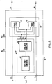
- FIG. 2 is a block diagram of interface circuit 12 showing the reference generator 20 in further detail.
- Reference generator 20 includes a trip point generator 42 and a simulated translator 46. Also shown in Figure 2 are a pair of actual translator circuits 24 and N.
- the reference generator 20 provides each of translators 24 and N with the three control voltages on lines 36, 38, and 40.
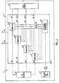
- FIG. 3 is a detailed circuit schematic of the reference generator 20 coupled to a single translator circuit 24.
- the trip point generator circuit 42 is connected to receive an input signal Vref supplied on line 34. From this input signal, the combined trip point generator 42 and simulated translator 46 supply the control voltages on lines 36, 38, and 40.
- the translator circuit 24 receives an ECL level input signal on line 30, and with the control voltages, supplies a CMOS level output signal on line 32.
- the first control voltage on line 40 is applied to the N-well 58 of PMOS transistor 50 to force the threshold characteristics of transistor 50 to match the base-emitter characteristics of a bipolar transistor.
- transistor 50 would always be on if
- Vthreshold is the threshold voltage for transistor 50
- Vbe is the base-emitter voltage of a bipolar transistor, approximately 0.8 volts.
- N-well 58 tied to upper power supply Vcc as would normally be the case, Vthreshold for transistor 50 could vary considerably as a result of production variations.
- a second control voltage on line 36 is applied to gate 62 of second PMOS transistor 60 in the translator.
- the second control voltage is approximately 0.8 volts below the "low" level of the ECL input on line 30.
- the second control voltage is therefore approximately (Vcc - 2.4 - 0.8) volts, or (Vcc - 3.4) volts.
- the second control voltage forces transistor 60 to have a trip point equal to the desired trip point, -1.6 volts in the preferred embodiment.
- a third control voltage on line 38 is applied to gate 72 of current source transistor 70, and to gate 82 of current source transistor 80.
- the third control voltage is a function of the characteristics of the NMOS and PMOS transistors.
- the third control voltage becomes relatively more positive if the PMOS transistors increase in conductivity (due to lower threshold voltage, or shorter electrical channel length, higher transconductance, thinner gate oxide layer) and becomes more negative when the PMOS transistors decrease in conductivity, etc.
- the current source transistors 70 and 80 are identical and operate as mirrored current sources, supplying current proportional to the third control voltage.
- translator circuit 24 The operation of translator circuit 24 is as follows. PMOS transistor 50, flip-flop transistor 90, current source transistor 70 are serially connected. Similarly, PMOS transistor 60, flip-flop transistor 100, and current source transistor 80 are also serially connected. As the following analysis will demonstrate, when PMOS transistor 50 is “on”, second PMOS transistor 60 and flip-flop transistor 90 are “off”. When PMOS transistor 60 is off, series flip-flop transistor 100 is “on”. No DC current is drawn at steady state because one flip-flop transistor 90 or 100 will always be "off", blocking the flow of DC current.
- source 64 is at potential (Vcc - 0.8) volts, while the gate 62 is at (Vcc - 2.4 - Vthreshold) by the control voltage on line 36.
- ⁇ 1.6 volts, transistor 60 will be on. Because Vthreshold is approximately -0.8 volts, this condition is readily met.
- transistor 60 With transistor 60 on, the voltage at its drain 66 and source 64 are equal, namely the "high" level on line 30, (Vcc - 0.8) volts. Drain 66 is connected to gate 92 of transistor 90, and as drain 66 rises toward (Vcc - 0.8) volts, gate 92 of transistor 90 rises. As gate 92 rises, transistor 90 turns on because the voltage at gate 92 (Vcc - 0.8) volts is at least a threshold voltage greater than the voltage at source 94. Although transistor 90 is on, the portion of circuit 24 consisting of transistors 50, 90, and 70 draws no DC current because transistor 50 is off. Similarly, transistors 60, 100 and 80 are connected in series. Although transistor 60 is on, transistor 100 is off and therefore no DC current is drawn through the series.
- Transistors 90 and 100 are connected together as a latch flip-flop with gate 102 of transistor 100 connected to drain 96 of transistor 90, and gate 92 of transistor 90 connected to drain 106 of transistor 100. Transistor 100 is off because as transistor 90 turns on, its drain 96 approaches Vee. When gate 102 is pulled down to Vee by drain 96 of transistor 90, transistor 100 will have zero gate-source voltage and will be off.
- PMOS transistor 50 will have a gate-source voltage equal to -2.4 volts. Because this gate-source voltage exceeds the threshold voltage dictated by the first control voltage on line 40, PMOS transistor 50 will turn on. As transistor 50 turns on, its drain 56 rises toward upper supply Vcc, turning on flip-flop transistor 100 and turning off transistor 90. Simultaneously, the second control voltage on line 36 causes PMOS transistor 60 to turn off because its gate-source potential is less than Vthreshold. Therefore, when the ECL input on line 30 is "low", transistors 50 and 100 are on.
- translator circuit 24 has translated an ECL “low” input on line 30 to a CMOS “low” level output on line 32, while drawing no steady-state current.
- the reference generator portion 20 of Figure 3 generates the three control voltages.
- the voltage trip point is made to be the desired DC level at which the actual translators should trip.
- the trip point is set to within approximately 50 mV of the midpoint between an ECL level "high” and "low".
- the trip point voltage from generator 42 is provided as a DC input signal to the "simulated" translator 46, whereupon the transistors comprising simulated translator 46 assume certain bias voltages.
- the transistors in the simulated translator are identical to the transistors in the translator. Therefore, the bias voltage present in "simulated" translator 46 are identical to the bias voltages that would exist in an actual translator when presented with an ECL input level equal to the trip point voltage.
- bias voltage established in the simulated translator 46 are used as control voltages and are applied to corresponding bias points in each of the plurality of translator circuits.
- Three bias points in the simulated translator are fed to similar bias points in the translators as first, second and third control voltages.
- each translator is forced to have a trip point equal to that established by the trip point generator.
- Trip point generator 42 receives an input reference voltage Vref on line 34.
- Reference voltage Vref on line 34 is a stable reference voltage, approximately 1.25 volts above Vee.
- Vref is supplied from the Reference Voltage Generator 10 which is the subject of a co-pending European Patent Application.
- Vref is applied to base 152 of transistor 150 to establish a known current through emitter resistor 158 equal to (Vref - Vbe - Vee)/(resistor 158), where Vbe is the base-emitter voltage drop of transistor 150.
- a known collector current flows through resistor 159, and the voltage drop across resistor 159 is made to be approximately 0.85 volts.
- Transistor 160 acts as an emitter follower and the voltage at its emitter 164 will be the voltage at its base 162 less a Vbe voltage drop.
- the voltage at emitter 164 is approximately two base-emitter voltage drops below upper power supply Vcc, i.e., the desired trip point.
- Transistor 170 acts as a load for emitter 164 and has its gate 172 tied to base 162 of transistor 160, its drain 176 tied to emitter 164, and its source 174 tied to lower supply Vee.
- the trip point voltage established by trip point voltage generator 42 is presented as an input signal to simulated translator 46.
- Simulated translator 46 includes PMOS transistors 180 and 200, current source transistors 190 and 220, and NMOS transistor 210.
- the desired trip point voltage at emitter 164 of transistor 160 is tied to gate 202 of PMOS transistor 200, while source 204 is tied to Vcc on line 14.
- PMOS transistor 200 is on because its gate 202 is approximately 1.5 volts more negative than source 204.
- the current from transistor 200 through transistor 220 is mirrored by current source transistor 190.
- NMOS transistor 210 has its gate 212 tied to gate 202 of transistor 200, and its drain 216 tied to drain 206 of transistor 200, and to gates 222 and 192 of current source transistors 220 and 190, respectively.
- Source 214 of transistor 210 is connected to drain 226 of first current source transistor 220.
- the bias voltage established within simulated translator 46 corresponds to the bias voltages present in an actual translator 22 whose ECL input signal is at a level equal to the trip point established by trip point generator 42.
- the ECL-CMOS interface circuit 12 typically is fabricated on the same die as the biCMOS circuit for which it provides ECL to CMOS interface translation.
Landscapes
- Engineering & Computer Science (AREA)
- Physics & Mathematics (AREA)
- Computer Hardware Design (AREA)
- Computing Systems (AREA)
- General Engineering & Computer Science (AREA)
- Mathematical Physics (AREA)
- Microelectronics & Electronic Packaging (AREA)
- Nonlinear Science (AREA)
- Electromagnetism (AREA)
- General Physics & Mathematics (AREA)
- Radar, Positioning & Navigation (AREA)
- Automation & Control Theory (AREA)
- Power Engineering (AREA)
- Logic Circuits (AREA)
Applications Claiming Priority (2)
| Application Number | Priority Date | Filing Date | Title |
|---|---|---|---|
| US07/151,347 US4855624A (en) | 1988-02-02 | 1988-02-02 | Low-power bipolar-CMOS interface circuit |
| US151347 | 1988-02-02 |
Publications (2)
| Publication Number | Publication Date |
|---|---|
| EP0326952A2 true EP0326952A2 (fr) | 1989-08-09 |
| EP0326952A3 EP0326952A3 (fr) | 1990-03-21 |
Family
ID=22538352
Family Applications (1)
| Application Number | Title | Priority Date | Filing Date |
|---|---|---|---|
| EP89101383A Ceased EP0326952A3 (fr) | 1988-02-02 | 1989-01-27 | Circuit d'interface bipolaire-CMOS |
Country Status (5)
| Country | Link |
|---|---|
| US (1) | US4855624A (fr) |
| EP (1) | EP0326952A3 (fr) |
| JP (1) | JPH0220919A (fr) |
| KR (1) | KR890013767A (fr) |
| CA (1) | CA1293777C (fr) |
Cited By (2)
| Publication number | Priority date | Publication date | Assignee | Title |
|---|---|---|---|---|
| EP0451365A3 (en) * | 1990-03-29 | 1991-11-06 | Siemens Aktiengesellschaft | Level converter |
| EP0765038A3 (fr) * | 1995-07-27 | 1998-01-07 | Texas Instruments Incorporated | Améliorations concernant la conception d'un inverseur CMOS |
Families Citing this family (6)
| Publication number | Priority date | Publication date | Assignee | Title |
|---|---|---|---|---|
| JPH0626309B2 (ja) * | 1988-07-22 | 1994-04-06 | 株式会社東芝 | 出力回路 |
| US5019726A (en) * | 1989-10-13 | 1991-05-28 | Advanced Micro Devices, Inc. | BiCMOS ECL-to-CMOS conversion circuit |
| US5160859A (en) * | 1990-10-22 | 1992-11-03 | National Semiconductor Corporation | Synchronous internal clock distribution |
| US5155391A (en) * | 1990-10-22 | 1992-10-13 | National Semiconductor Corporation | Synchronous internal clock distribution |
| US5204557A (en) * | 1991-10-15 | 1993-04-20 | National Semiconductor Corporation | Digital signal level translator |
| US5367210A (en) * | 1992-02-12 | 1994-11-22 | Lipp Robert J | Output buffer with reduced noise |
Family Cites Families (8)
| Publication number | Priority date | Publication date | Assignee | Title |
|---|---|---|---|---|
| US3916430A (en) * | 1973-03-14 | 1975-10-28 | Rca Corp | System for eliminating substrate bias effect in field effect transistor circuits |
| US4430582A (en) * | 1981-11-16 | 1984-02-07 | National Semiconductor Corporation | Fast CMOS buffer for TTL input levels |
| US4453095A (en) * | 1982-07-16 | 1984-06-05 | Motorola Inc. | ECL MOS Buffer circuits |
| JPS5943631A (ja) * | 1982-09-06 | 1984-03-10 | Hitachi Ltd | レベル変換入力回路 |
| US4645951A (en) * | 1983-08-31 | 1987-02-24 | Hitachi, Ltd. | Semiconductor integrated circuit having a C-MOS internal logic block and an output buffer for providing ECL level signals |
| US4555642A (en) * | 1983-09-22 | 1985-11-26 | Standard Microsystems Corporation | Low power CMOS input buffer circuit |
| US4642488A (en) * | 1985-09-03 | 1987-02-10 | Codex Corporation | CMOS input buffer accepting TTL level inputs |
| US4645954A (en) * | 1985-10-21 | 1987-02-24 | International Business Machines Corp. | ECL to FET interface circuit for field effect transistor arrays |
-
1988
- 1988-02-02 US US07/151,347 patent/US4855624A/en not_active Expired - Lifetime
-
1989
- 1989-01-27 EP EP89101383A patent/EP0326952A3/fr not_active Ceased
- 1989-02-01 CA CA000589776A patent/CA1293777C/fr not_active Expired - Fee Related
- 1989-02-02 KR KR1019890001193A patent/KR890013767A/ko not_active Abandoned
- 1989-02-02 JP JP1022723A patent/JPH0220919A/ja active Pending
Cited By (2)
| Publication number | Priority date | Publication date | Assignee | Title |
|---|---|---|---|---|
| EP0451365A3 (en) * | 1990-03-29 | 1991-11-06 | Siemens Aktiengesellschaft | Level converter |
| EP0765038A3 (fr) * | 1995-07-27 | 1998-01-07 | Texas Instruments Incorporated | Améliorations concernant la conception d'un inverseur CMOS |
Also Published As
| Publication number | Publication date |
|---|---|
| JPH0220919A (ja) | 1990-01-24 |
| EP0326952A3 (fr) | 1990-03-21 |
| KR890013767A (ko) | 1989-09-25 |
| CA1293777C (fr) | 1991-12-31 |
| US4855624A (en) | 1989-08-08 |
Similar Documents
| Publication | Publication Date | Title |
|---|---|---|
| US4437171A (en) | ECL Compatible CMOS memory | |
| US4663584A (en) | Intermediate potential generation circuit | |
| KR910004651B1 (ko) | 레벨 변환 입력 회로 | |
| US6437627B1 (en) | High voltage level shifter for switching high voltage in non-volatile memory intergrated circuits | |
| US6040729A (en) | Digital output buffer for multiple voltage system | |
| KR0132053B1 (ko) | 반도체집적회로장치 및 그 조합전자장치 | |
| EP0231062A1 (fr) | Circuit de conversion de niveau | |
| KR910006696B1 (ko) | 출력 인터페이스회로 | |
| EP0473138A2 (fr) | Générateur VCC/2 de faible puissance | |
| US6072354A (en) | Semiconductor device output buffer circuit for LSI | |
| JPH0436606B2 (fr) | ||
| US5214317A (en) | CMOS to ECL translator with incorporated latch | |
| US5731713A (en) | TTL to CMOS level translator with voltage and threshold compensation | |
| US6201436B1 (en) | Bias current generating circuits and methods for integrated circuits including bias current generators that increase and decrease with temperature | |
| KR0126911B1 (ko) | 기준전압 발생회로 및 발생방법 | |
| EP0383095B1 (fr) | Réseau de référence bicmos | |
| US4855624A (en) | Low-power bipolar-CMOS interface circuit | |
| US20020017943A1 (en) | Voltage level converter circuit improved in operation reliability | |
| US6753707B2 (en) | Delay circuit and semiconductor device using the same | |
| KR0138949B1 (ko) | 씨모스 회로와 바이폴라 회로가 혼재되어 있는 반도체 디바이스 | |
| US5225716A (en) | Semiconductor integrated circuit having means for suppressing a variation in a threshold level due to temperature variation | |
| JPH08251007A (ja) | BiCMOS論理ゲート回路 | |
| US5945843A (en) | Semiconductor integrated circuit | |
| US5942923A (en) | Low-voltage output driving circuit having pull-up transistor with comparator controlled gate | |
| US5361004A (en) | TTL-CMOS output stage for an integrated circuit |
Legal Events
| Date | Code | Title | Description |
|---|---|---|---|
| PUAI | Public reference made under article 153(3) epc to a published international application that has entered the european phase |
Free format text: ORIGINAL CODE: 0009012 |
|
| AK | Designated contracting states |
Kind code of ref document: A2 Designated state(s): DE FR GB IT NL |
|
| PUAL | Search report despatched |
Free format text: ORIGINAL CODE: 0009013 |
|
| AK | Designated contracting states |
Kind code of ref document: A3 Designated state(s): DE FR GB IT NL |
|
| 17P | Request for examination filed |
Effective date: 19900717 |
|
| 17Q | First examination report despatched |
Effective date: 19920729 |
|
| STAA | Information on the status of an ep patent application or granted ep patent |
Free format text: STATUS: THE APPLICATION HAS BEEN REFUSED |
|
| 18R | Application refused |
Effective date: 19951203 |