EP0326954A2 - Bipolare CMOS-Leistungsübergangsschaltung - Google Patents
Bipolare CMOS-Leistungsübergangsschaltung Download PDFInfo
- Publication number
- EP0326954A2 EP0326954A2 EP89101404A EP89101404A EP0326954A2 EP 0326954 A2 EP0326954 A2 EP 0326954A2 EP 89101404 A EP89101404 A EP 89101404A EP 89101404 A EP89101404 A EP 89101404A EP 0326954 A2 EP0326954 A2 EP 0326954A2
- Authority
- EP
- European Patent Office
- Prior art keywords
- circuit
- monitoring
- transistor
- signal
- inverter
- Prior art date
- Legal status (The legal status is an assumption and is not a legal conclusion. Google has not performed a legal analysis and makes no representation as to the accuracy of the status listed.)
- Withdrawn
Links
Images

Classifications
-
- G—PHYSICS
- G11—INFORMATION STORAGE
- G11C—STATIC STORES
- G11C11/00—Digital stores characterised by the use of particular electric or magnetic storage elements; Storage elements therefor
- G11C11/21—Digital stores characterised by the use of particular electric or magnetic storage elements; Storage elements therefor using electric elements
- G11C11/34—Digital stores characterised by the use of particular electric or magnetic storage elements; Storage elements therefor using electric elements using semiconductor devices
- G11C11/40—Digital stores characterised by the use of particular electric or magnetic storage elements; Storage elements therefor using electric elements using semiconductor devices using transistors
- G11C11/401—Digital stores characterised by the use of particular electric or magnetic storage elements; Storage elements therefor using electric elements using semiconductor devices using transistors forming cells needing refreshing or charge regeneration, i.e. dynamic cells
- G11C11/4063—Auxiliary circuits, e.g. for addressing, decoding, driving, writing, sensing or timing
- G11C11/407—Auxiliary circuits, e.g. for addressing, decoding, driving, writing, sensing or timing for memory cells of the field-effect type
- G11C11/4074—Power supply or voltage generation circuits, e.g. bias voltage generators, substrate voltage generators, back-up power, power control circuits
-
- H—ELECTRICITY
- H03—ELECTRONIC CIRCUITRY
- H03K—PULSE TECHNIQUE
- H03K17/00—Electronic switching or gating, i.e. not by contact-making and –breaking
- H03K17/22—Modifications for ensuring a predetermined initial state when the supply voltage has been applied
- H03K17/223—Modifications for ensuring a predetermined initial state when the supply voltage has been applied in field-effect transistor switches
-
- G—PHYSICS
- G11—INFORMATION STORAGE
- G11C—STATIC STORES
- G11C5/00—Details of stores covered by group G11C11/00
- G11C5/14—Power supply arrangements, e.g. power down, chip selection or deselection, layout of wirings or power grids, or multiple supply levels
-
- H—ELECTRICITY
- H10—SEMICONDUCTOR DEVICES; ELECTRIC SOLID-STATE DEVICES NOT OTHERWISE PROVIDED FOR
- H10D—INORGANIC ELECTRIC SEMICONDUCTOR DEVICES
- H10D84/00—Integrated devices formed in or on semiconductor substrates that comprise only semiconducting layers, e.g. on Si wafers or on GaAs-on-Si wafers
- H10D84/80—Integrated devices formed in or on semiconductor substrates that comprise only semiconducting layers, e.g. on Si wafers or on GaAs-on-Si wafers characterised by the integration of at least one component covered by groups H10D12/00 or H10D30/00, e.g. integration of IGFETs
- H10D84/82—Integrated devices formed in or on semiconductor substrates that comprise only semiconducting layers, e.g. on Si wafers or on GaAs-on-Si wafers characterised by the integration of at least one component covered by groups H10D12/00 or H10D30/00, e.g. integration of IGFETs of only field-effect components
- H10D84/83—Integrated devices formed in or on semiconductor substrates that comprise only semiconducting layers, e.g. on Si wafers or on GaAs-on-Si wafers characterised by the integration of at least one component covered by groups H10D12/00 or H10D30/00, e.g. integration of IGFETs of only field-effect components of only insulated-gate FETs [IGFET]
- H10D84/85—Complementary IGFETs, e.g. CMOS
Definitions
- This invention relates to electronic circuit severelyry, and more particularly to circuitry for protecting bipolar-complementary metal oxide semiconductor (BiCMOS) circuits during power transitions.
- BiCMOS bipolar-complementary metal oxide semiconductor
- circuits having both bipolar and MOS devices particularly require protection because the bipolar devices and the MOS devices have different characteristics during power transitions.
- data in a BiCMOS static RAM is stored in a plurality of flip-flops which are individually selected for reading or writing information.
- the voltage levels present during a power transition may be sufficient to turn-on the CMOS transistors, but leave the bipolar transistors in the circuit essentially off.
- the output levels of the substantially off bipolar transistors appear to the remainder of the circuit as legitimately "high".
- the unintended high outputs may cause the CMOS devices in the circuit to enter undefined states in a BiCMOS memory device. These undefined states can cause data loss or multiple selects with resultant high current and potential damage to the BiCMOS chip.
- CMOS devices are active at lower voltage levels than the bipolar transistors, once the bipolar transistors are active, all of the semiconductors in the BiCMOS circuit will be active. It is only necessary, therefore, to disable or protect the BiCMOS circuit until the bipolar transistors are active.
- a BiCMOS protection circuit is constructed on the same chip as the BiCMOS circuit which is being protected.
- the present invention provides a circuit which generates a first reference input signal proportional to the upper power supply in the protected circuit and a second reference input signal proportional to the lower power supply in the protected circuit.
- the protection circuit determines from the first and second reference input signals whether a power transition is occurring. If a transition is occurring, the protection circuit supplies an output that disables memory row decoders and write logic in the BiCMOS memory circuit.
- the present invention allows an independent input signal to override a determination that no power transition exists, and nonetheless protect the BiCMOS circuit.
- the present invention provides automatic protection without operator intervention.
- the output signal from the power transition circuit protects the BiCMOS circuit.
- the BiCMOS circuit automatically resumes normal operation.
- Figure 1 shows a semiconductor die 1 that includes a BiCMOS circuit 150 to be protected, a generator circuit 140 and a power transition circuit 2.
- Die 1 receives upper power supply voltage Vcc on line 130 and lower power supply voltage Vee on line 136.
- Power transition circuit 2 protects circuit 150 during power transitions.
- Circuit 2 includes a monitoring circuit 3 and a disabling circuit 4.
- Generator circuit 140 provides input signals on lines 5, 6 to the monitoring circuit 3, and a third input signal on line 7 to the disabling circuit 4. From the two input signals on lines 5 and 6, the monitoring circuit 3 determines whether a power transition is occurring and therefore whether to disable BiCMOS circuit 150. If disabling is required, then circuit 4 causes output signal Pup on line 8 to be "0", otherwise Pup is "1".
- the third input signal on line 7 is connected directly to the disabling circuit and causes output signal Pup to be "0" whenever the third signal is present.
- protected circuit 150 is a BiCMOS SRAM.
- output Pup on line 8 is "0"
- circuitry within BiCMOS SRAM 150 disables the SRAM memory row decoders (not shown) and write logic functions (not shown).
- a complementary output signal Pupb is supplied on line 9 to protected BiCMOS circuit 150.
- Generator 140 provides two signals to determining circuit 3--first reference Vref+ on line 5 and second reference Vref on line 6.
- An independent input signal Vcsm on line 7 is supplied directly to disabling circuit 4.
- Signal Vref+ is proportional to the upper power supply Vcc on line 130, while signal Vref is proportional to lower power supply Vee on line 136.
- Determining circuit 3 relies upon the difference in potential between Vref and Vref+ in deciding whether power to BiCMOS circuit 150 is in transition.
- Signal Vcsm is any signal whose presence the system designer wishes to cause protection of BiCMOS circuit 150.
- Vref+ and Vref are obtained from a generator disclosed in a co-pending European Patent Application. It is sufficient to note that Vref is the reference voltage at approximately 1.25 volts more positive than lower power supply Vee. Vref+, in turn, is approximately 1 volt less than upper power supply Vcc. Input Vcsm is supplied from a generator such as disclosed in a co-pending European Patent Application.
- BiCMOS circuits which include emitter coupled logic (ECL) circuits
- the bipolar transistors are active when Vref+ is 0.3 volts more positive than Vref.
- determining circuit 3 causes disabling circuit 4 to make output Pup on line 8 to be "0", thus disabling circuit 150.
- ECL emitter coupled logic
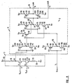
- FIG. 2 is a detailed schematic of the power transition circuit 2.
- Circuit 2 includes the determining circuit 3 and the disabling circuit 4.
- Determining circuit 3 receives signal Vref+ on line 5 and signal Vref on line 6.
- Signal Vref+ on line 5 is connected to base 12 of bipolar transistor 10, and signal Vref on line 6 is connected to base 22 of bipolar transistor 20.
- Collector 26 of transistor 20 is connected to emitter 14 of transistor 10, thereby placing transistor 20 in series with transistor 10.
- signal Vref on line 6 When the power supplies Vcc and Vee are turned on, signal Vref on line 6 will reach a level sufficient to turn on transistor 20 before signal Vref+ on line 5 reaches a level sufficient to turn on transistor 10.
- transistor 20 When transistor 20 turns on, current from emitter 24 flows into resistor 28, and transistor 20 will try to saturate.
- the voltage at emitter 24 will be approximately (Vref - 0.7) volts, and the voltage at collector 26 will be approximately 0.3 volts (one collector-emitter voltage drop) more positive than the voltage at emitter 24. Therefore, the voltage at emitter 14 is approximately (Vref - 0.7 + 0.3) volts or (Vref - 0.4) volts.
- transistor 10 For transistor 10 to become active, the voltage at base 12, Vref+, must exceed the voltage at emitter 14 by at least 0.7 volts. Therefore, transistor 10 turns on only when Vref+ > 0.7 + (Vref - 0.4) volts, or when Vref+ > Vref + 0.3 volts.
- the condition Vref+ ⁇ Vref + 0.3 volts is referred to herein as the "proper" Vref+, Vref relationship.
- transistors 10 and 20 are in series, no current flows through resistor 18 until both transistors 10 and 20 are on. Current flow through resistor 18 therefore signifies no power transition, i.e., Vref+ ⁇ Vref + 0.3 volts.
- Transistors 10 and 20 thus provide a NAND function on input signals Vref+ and Vref.
- the voltage at collector 16 is relatively low when the proper Vref+, Vref relationship exists, and is relatively high when the relationship does not exist.
- Collector 16 is connected to the gates 32, 42 of PMOS transistor 30 and NMOS transistor 40 in the disabling circuit.
- the output of the inverter 35 formed by transistors 30 and 40 is node 37.
- node 37 is at a CMOS "1" level.
- the signal at node 37 is thus analogous to an AND function of Vref+ and Vref.
- Node 37 is connected to gate 52 of PMOS transistor 50 and to gate 82 of NMOS transistor 80.
- Transistor 50 is connected as an inverter, with source 54 tied to power supply Vcc on line 130 and with drain 56 tied to drains 66, 74 of transistors 60 and 70.
- transistor 80 is turned on and allows transistor 60 and 70 to function.
- Transistors 60 and 70 are respectively PMOS and NMOS devices whose respective gates 62, 72 and drains 66, 74 are tied together to create another inverter 65.
- Transistors 90 and 100 have their respective gates 92, 102 and drains 96, 104 tied together to form another inverter 95.
- Signal Vcsm on line 7 is connected to the inverter 95.
- Vcsm is a user specified signal employed to disable BiCMOS circuit 150 when Vcsm is a "1", i.e., when the output signal at node 97 is a "0".
- the circuit shown in Figure 2 operates as follows. If a power transition is occurring and the user specified enable signal Vcsm is active, node 16 will be low and input signal Vcsm will be high. Thus, node 37 will be high and node 97 low. Thus, nodes 62, 72 of inverter 65 are "0" and the output of inverter 65 at node 67 is "1". Because gate 52 of transistor 50 is “high” and source 54 is “high”, transistor 50 is off, and does not affect the output of inverter 65 at node 67 which maintains a "1". Inverter 115 inverts the output of inverter 65 at node 67. Therefore, the output of inverter 115, output Pup on line 8, is a "0", disabling the protected circuit.
- Vcsm on line 7 is "0" (i.e., no disable required), but that the Vref+, Vref relationship is not proper.
- the improper Vref+, Vref relationship places a "0" at node 37.
- Transistor 80 is turned off and renders inverter 65 inoperative.
- Vcsm is "0” and the output of inverter 95 at node 97 is “1".
- the "1" output from inverter 95 does not change the output of inverter 65 at node 67 because transistor 80 is off.
- Vcsm will not affect the output signal from inverter 65.
- the "0" output from inverter 35 turns transistor 50 on, pulling the output of inverter 65 at node 67 up to "1".
- drain 66 of transistor 60 is tied to the output of inverter 65 at node 67, node 67 is pulled up to a "1". Therefore, the output of inverter 115, Pup on line 8, will be a "0", protecting BiCMOS circuit 150.
Landscapes
- Engineering & Computer Science (AREA)
- Power Engineering (AREA)
- Microelectronics & Electronic Packaging (AREA)
- Computer Hardware Design (AREA)
- Logic Circuits (AREA)
- Semiconductor Integrated Circuits (AREA)
- Metal-Oxide And Bipolar Metal-Oxide Semiconductor Integrated Circuits (AREA)
- Electronic Switches (AREA)
Applications Claiming Priority (2)
| Application Number | Priority Date | Filing Date | Title |
|---|---|---|---|
| US151346 | 1988-02-02 | ||
| US07/151,346 US4980792A (en) | 1988-02-02 | 1988-02-02 | BiCMOS power transition circuit |
Publications (2)
| Publication Number | Publication Date |
|---|---|
| EP0326954A2 true EP0326954A2 (de) | 1989-08-09 |
| EP0326954A3 EP0326954A3 (de) | 1991-02-27 |
Family
ID=22538347
Family Applications (1)
| Application Number | Title | Priority Date | Filing Date |
|---|---|---|---|
| EP19890101404 Withdrawn EP0326954A3 (de) | 1988-02-02 | 1989-01-27 | Bipolare CMOS-Leistungsübergangsschaltung |
Country Status (5)
| Country | Link |
|---|---|
| US (1) | US4980792A (de) |
| EP (1) | EP0326954A3 (de) |
| JP (1) | JPH025457A (de) |
| KR (1) | KR890013768A (de) |
| CA (1) | CA1314077C (de) |
Families Citing this family (8)
| Publication number | Priority date | Publication date | Assignee | Title |
|---|---|---|---|---|
| US5294883A (en) * | 1992-08-04 | 1994-03-15 | International Business Machines Corporation | Test detector/shutoff and method for BiCMOS integrated circuit |
| DE69412891T2 (de) * | 1993-04-19 | 1999-04-01 | Koninklijke Philips Electronics N.V., Eindhoven | Überspannungsschutzschaltung |
| US5473500A (en) * | 1994-01-13 | 1995-12-05 | Atmel Corporation | Electrostatic discharge circuit for high speed, high voltage circuitry |
| FR2729762A1 (fr) * | 1995-01-23 | 1996-07-26 | Sgs Thomson Microelectronics | Circuit de detection de tension compense en technologie et en temperature |
| US5625280A (en) * | 1995-10-30 | 1997-04-29 | International Business Machines Corp. | Voltage regulator bypass circuit |
| JP3464340B2 (ja) * | 1996-04-19 | 2003-11-10 | 沖電気工業株式会社 | 半導体集積回路装置 |
| KR100282708B1 (ko) * | 1997-12-04 | 2001-02-15 | 윤종용 | 반도체 장치의 입력 회로 (input circuit of semiconductor device) |
| JP3022815B2 (ja) * | 1997-07-24 | 2000-03-21 | 日本電気アイシーマイコンシステム株式会社 | 中間電位生成回路 |
Family Cites Families (11)
| Publication number | Priority date | Publication date | Assignee | Title |
|---|---|---|---|---|
| US4086503A (en) * | 1976-06-21 | 1978-04-25 | Westinghouse Electric Corporation | Control circuit initiating conduction of an opto-isolator unit |
| JPS5326175A (en) * | 1976-08-23 | 1978-03-10 | Seiko Instr & Electronics Ltd | Electronic watch |
| US4096560A (en) * | 1977-10-28 | 1978-06-20 | Rockwell International Corporation | Protection circuit to minimize the effects of power line interruptions on the contents of a volatile electronic memory |
| US4301380A (en) * | 1979-05-01 | 1981-11-17 | Motorola, Inc. | Voltage detector |
| US4375663A (en) * | 1980-03-31 | 1983-03-01 | Leeds & Northrup Company | Power failure early warning circuit for microprocessor with CMOS RAM memory |
| DE3035896C2 (de) * | 1980-09-24 | 1984-02-09 | Robert Bosch Gmbh, 7000 Stuttgart | Schaltungsanordnung zur Erzeugung von Impulen bei Störung der Stromversorgung |
| US4473759A (en) * | 1982-04-22 | 1984-09-25 | Motorola, Inc. | Power sensing circuit and method |
| US4594517A (en) * | 1984-04-30 | 1986-06-10 | Rca Corporation | Power down sensor |
| JPS6146613A (ja) * | 1984-08-10 | 1986-03-06 | Nec Corp | レベル検出回路 |
| US4685023A (en) * | 1986-11-14 | 1987-08-04 | General Motors Corporation | Power latch circuit for computer self deactivation |
| FR2616602B1 (fr) * | 1987-06-12 | 1989-10-13 | Thomson Semiconducteurs | Circuit de remise sous tension pour circuit integre en technologie mos |
-
1988
- 1988-02-02 US US07/151,346 patent/US4980792A/en not_active Expired - Lifetime
-
1989
- 1989-01-27 EP EP19890101404 patent/EP0326954A3/de not_active Withdrawn
- 1989-02-01 CA CA000589771A patent/CA1314077C/en not_active Expired - Fee Related
- 1989-02-02 KR KR1019890001194A patent/KR890013768A/ko not_active Withdrawn
- 1989-02-02 JP JP1022724A patent/JPH025457A/ja active Pending
Also Published As
| Publication number | Publication date |
|---|---|
| JPH025457A (ja) | 1990-01-10 |
| US4980792A (en) | 1990-12-25 |
| CA1314077C (en) | 1993-03-02 |
| KR890013768A (ko) | 1989-09-25 |
| EP0326954A3 (de) | 1991-02-27 |
Similar Documents
| Publication | Publication Date | Title |
|---|---|---|
| US6448812B1 (en) | Pull up/pull down logic for holding a defined value during power down mode | |
| EP0141681B1 (de) | Schaltung zur Erfassung von Prüfeingaben | |
| US4441136A (en) | Switching circuit | |
| US5760624A (en) | Power-on reset circuit with hysteresis | |
| KR100312929B1 (ko) | 과전압보호회로를갖는전자장치 | |
| US6518746B2 (en) | Integrated circuit device having a burn-in mode for which entry into and exit from can be controlled | |
| JP2536871B2 (ja) | オフ・チップ駆動回路 | |
| US5019772A (en) | Test selection techniques | |
| US5781485A (en) | Apparatus and method for controlling operating mode in semiconductor memory device | |
| US6201431B1 (en) | Method and apparatus for automatically adjusting noise immunity of an integrated circuit | |
| US5124573A (en) | Adjustable clock chopper/expander circuit | |
| US5250854A (en) | Bitline pull-up circuit operable in a low-resistance test mode | |
| EP0583887A2 (de) | Ausgangspufferschaltungen | |
| US4980792A (en) | BiCMOS power transition circuit | |
| US5254885A (en) | Bi-CMOS logic circuit with feedback | |
| JP3311751B2 (ja) | 低電力型電圧感知回路 | |
| US5034687A (en) | Signature indicating circuit | |
| US5747890A (en) | Power supply switch reference circuitry | |
| US20030042946A1 (en) | Circuit to eliminate bus contention at chip power up | |
| US5173623A (en) | High performance BiCMOS logic circuits with full output voltage swing up to four predetermined voltage values | |
| KR100849121B1 (ko) | 전기 아이디 회로 및 방법 | |
| US5535166A (en) | Circuit for isolating and driving interconnect lines | |
| US6720821B2 (en) | Methods and systems for generating interim voltage supplies | |
| US5949797A (en) | Microcontroller test circuit | |
| US7589562B2 (en) | I/O cell capable of finely controlling drive strength |
Legal Events
| Date | Code | Title | Description |
|---|---|---|---|
| PUAI | Public reference made under article 153(3) epc to a published international application that has entered the european phase |
Free format text: ORIGINAL CODE: 0009012 |
|
| AK | Designated contracting states |
Kind code of ref document: A2 Designated state(s): DE FR GB IT NL |
|
| PUAL | Search report despatched |
Free format text: ORIGINAL CODE: 0009013 |
|
| AK | Designated contracting states |
Kind code of ref document: A3 Designated state(s): DE FR GB IT NL |
|
| 17P | Request for examination filed |
Effective date: 19910330 |
|
| 17Q | First examination report despatched |
Effective date: 19930210 |
|
| STAA | Information on the status of an ep patent application or granted ep patent |
Free format text: STATUS: THE APPLICATION IS DEEMED TO BE WITHDRAWN |
|
| 18D | Application deemed to be withdrawn |
Effective date: 19930821 |