EP0327121A2 - Transistor à effet champ à supraconducteur - Google Patents
Transistor à effet champ à supraconducteur Download PDFInfo
- Publication number
- EP0327121A2 EP0327121A2 EP89101951A EP89101951A EP0327121A2 EP 0327121 A2 EP0327121 A2 EP 0327121A2 EP 89101951 A EP89101951 A EP 89101951A EP 89101951 A EP89101951 A EP 89101951A EP 0327121 A2 EP0327121 A2 EP 0327121A2
- Authority
- EP
- European Patent Office
- Prior art keywords
- superconducting
- layer
- gate electrode
- electrodes
- field effect
- Prior art date
- Legal status (The legal status is an assumption and is not a legal conclusion. Google has not performed a legal analysis and makes no representation as to the accuracy of the status listed.)
- Withdrawn
Links
- 230000005669 field effect Effects 0.000 title claims abstract description 60
- 238000000034 method Methods 0.000 claims abstract description 44
- 238000004519 manufacturing process Methods 0.000 claims abstract description 21
- 239000000758 substrate Substances 0.000 claims description 103
- 229910052581 Si3N4 Inorganic materials 0.000 claims description 58
- HQVNEWCFYHHQES-UHFFFAOYSA-N silicon nitride Chemical compound N12[Si]34N5[Si]62N3[Si]51N64 HQVNEWCFYHHQES-UHFFFAOYSA-N 0.000 claims description 58
- 229910021420 polycrystalline silicon Inorganic materials 0.000 claims description 51
- 239000004065 semiconductor Substances 0.000 claims description 39
- 239000000463 material Substances 0.000 claims description 37
- 239000010955 niobium Substances 0.000 claims description 29
- 229910052758 niobium Inorganic materials 0.000 claims description 25
- GUCVJGMIXFAOAE-UHFFFAOYSA-N niobium atom Chemical compound [Nb] GUCVJGMIXFAOAE-UHFFFAOYSA-N 0.000 claims description 25
- 230000015572 biosynthetic process Effects 0.000 claims description 3
- 150000003377 silicon compounds Chemical class 0.000 claims description 2
- VYPSYNLAJGMNEJ-UHFFFAOYSA-N Silicium dioxide Chemical compound O=[Si]=O VYPSYNLAJGMNEJ-UHFFFAOYSA-N 0.000 description 35
- 238000007254 oxidation reaction Methods 0.000 description 15
- 238000001020 plasma etching Methods 0.000 description 15
- IJGRMHOSHXDMSA-UHFFFAOYSA-N Atomic nitrogen Chemical compound N#N IJGRMHOSHXDMSA-UHFFFAOYSA-N 0.000 description 14
- 229910052681 coesite Inorganic materials 0.000 description 14
- 229910052906 cristobalite Inorganic materials 0.000 description 14
- 230000003647 oxidation Effects 0.000 description 14
- 239000000377 silicon dioxide Substances 0.000 description 14
- 235000012239 silicon dioxide Nutrition 0.000 description 14
- 229910052682 stishovite Inorganic materials 0.000 description 14
- 229910052905 tridymite Inorganic materials 0.000 description 14
- QVGXLLKOCUKJST-UHFFFAOYSA-N atomic oxygen Chemical compound [O] QVGXLLKOCUKJST-UHFFFAOYSA-N 0.000 description 13
- 239000001301 oxygen Substances 0.000 description 13
- 229910052760 oxygen Inorganic materials 0.000 description 13
- 239000007789 gas Substances 0.000 description 12
- 229920002120 photoresistant polymer Polymers 0.000 description 9
- 238000003486 chemical etching Methods 0.000 description 8
- 238000005229 chemical vapour deposition Methods 0.000 description 8
- 230000000694 effects Effects 0.000 description 8
- KRHYYFGTRYWZRS-UHFFFAOYSA-N Fluorane Chemical compound F KRHYYFGTRYWZRS-UHFFFAOYSA-N 0.000 description 7
- XUIMIQQOPSSXEZ-UHFFFAOYSA-N Silicon Chemical compound [Si] XUIMIQQOPSSXEZ-UHFFFAOYSA-N 0.000 description 7
- 229960002050 hydrofluoric acid Drugs 0.000 description 7
- 229910052757 nitrogen Inorganic materials 0.000 description 7
- 229910052710 silicon Inorganic materials 0.000 description 7
- 239000010703 silicon Substances 0.000 description 7
- 229910052814 silicon oxide Inorganic materials 0.000 description 7
- 238000010894 electron beam technology Methods 0.000 description 6
- 238000000609 electron-beam lithography Methods 0.000 description 6
- ZOXJGFHDIHLPTG-UHFFFAOYSA-N Boron Chemical compound [B] ZOXJGFHDIHLPTG-UHFFFAOYSA-N 0.000 description 5
- 229910052796 boron Inorganic materials 0.000 description 5
- 239000013078 crystal Substances 0.000 description 5
- 238000005566 electron beam evaporation Methods 0.000 description 5
- 239000012535 impurity Substances 0.000 description 5
- 238000005468 ion implantation Methods 0.000 description 5
- CSCPPACGZOOCGX-UHFFFAOYSA-N Acetone Chemical compound CC(C)=O CSCPPACGZOOCGX-UHFFFAOYSA-N 0.000 description 4
- PNEYBMLMFCGWSK-UHFFFAOYSA-N Alumina Chemical compound [O-2].[O-2].[O-2].[Al+3].[Al+3] PNEYBMLMFCGWSK-UHFFFAOYSA-N 0.000 description 4
- MYMOFIZGZYHOMD-UHFFFAOYSA-N Dioxygen Chemical compound O=O MYMOFIZGZYHOMD-UHFFFAOYSA-N 0.000 description 4
- NBIIXXVUZAFLBC-UHFFFAOYSA-N Phosphoric acid Chemical compound OP(O)(O)=O NBIIXXVUZAFLBC-UHFFFAOYSA-N 0.000 description 4
- 229910052782 aluminium Inorganic materials 0.000 description 4
- -1 arsenic ions Chemical class 0.000 description 4
- 239000000969 carrier Substances 0.000 description 4
- VZGDMQKNWNREIO-UHFFFAOYSA-N tetrachloromethane Chemical compound ClC(Cl)(Cl)Cl VZGDMQKNWNREIO-UHFFFAOYSA-N 0.000 description 4
- XLYOFNOQVPJJNP-UHFFFAOYSA-N water Substances O XLYOFNOQVPJJNP-UHFFFAOYSA-N 0.000 description 4
- 241001669573 Galeorhinus galeus Species 0.000 description 3
- CPLXHLVBOLITMK-UHFFFAOYSA-N Magnesium oxide Chemical compound [Mg]=O CPLXHLVBOLITMK-UHFFFAOYSA-N 0.000 description 3
- XAGFODPZIPBFFR-UHFFFAOYSA-N aluminium Chemical compound [Al] XAGFODPZIPBFFR-UHFFFAOYSA-N 0.000 description 3
- 229910052785 arsenic Inorganic materials 0.000 description 3
- 238000000151 deposition Methods 0.000 description 3
- RWRIWBAIICGTTQ-UHFFFAOYSA-N difluoromethane Chemical compound FCF RWRIWBAIICGTTQ-UHFFFAOYSA-N 0.000 description 3
- 239000007788 liquid Substances 0.000 description 3
- 229910000978 Pb alloy Inorganic materials 0.000 description 2
- OAICVXFJPJFONN-UHFFFAOYSA-N Phosphorus Chemical compound [P] OAICVXFJPJFONN-UHFFFAOYSA-N 0.000 description 2
- 229910003097 YBa2Cu3O7−δ Inorganic materials 0.000 description 2
- 239000004411 aluminium Substances 0.000 description 2
- 229910000147 aluminium phosphate Inorganic materials 0.000 description 2
- RQNWIZPPADIBDY-UHFFFAOYSA-N arsenic atom Chemical group [As] RQNWIZPPADIBDY-UHFFFAOYSA-N 0.000 description 2
- 230000015556 catabolic process Effects 0.000 description 2
- 239000004020 conductor Substances 0.000 description 2
- 230000002349 favourable effect Effects 0.000 description 2
- 238000010438 heat treatment Methods 0.000 description 2
- 229910052738 indium Inorganic materials 0.000 description 2
- 150000002500 ions Chemical class 0.000 description 2
- 150000002822 niobium compounds Chemical class 0.000 description 2
- SIWVEOZUMHYXCS-UHFFFAOYSA-N oxo(oxoyttriooxy)yttrium Chemical compound O=[Y]O[Y]=O SIWVEOZUMHYXCS-UHFFFAOYSA-N 0.000 description 2
- 229910052698 phosphorus Inorganic materials 0.000 description 2
- 239000011574 phosphorus Substances 0.000 description 2
- 229920000642 polymer Polymers 0.000 description 2
- LIVNPJMFVYWSIS-UHFFFAOYSA-N silicon monoxide Chemical compound [Si-]#[O+] LIVNPJMFVYWSIS-UHFFFAOYSA-N 0.000 description 2
- 229910002076 stabilized zirconia Inorganic materials 0.000 description 2
- 229910052718 tin Inorganic materials 0.000 description 2
- 230000005641 tunneling Effects 0.000 description 2
- 229910052727 yttrium Inorganic materials 0.000 description 2
- VWQVUPCCIRVNHF-UHFFFAOYSA-N yttrium atom Chemical compound [Y] VWQVUPCCIRVNHF-UHFFFAOYSA-N 0.000 description 2
- YMWLPMGFZYFLRP-UHFFFAOYSA-N 2-(4,5-dimethyl-1,3-diselenol-2-ylidene)-4,5-dimethyl-1,3-diselenole Chemical compound [Se]1C(C)=C(C)[Se]C1=C1[Se]C(C)=C(C)[Se]1 YMWLPMGFZYFLRP-UHFFFAOYSA-N 0.000 description 1
- 229910000838 Al alloy Inorganic materials 0.000 description 1
- 229910000846 In alloy Inorganic materials 0.000 description 1
- 229910001128 Sn alloy Inorganic materials 0.000 description 1
- ATJFFYVFTNAWJD-UHFFFAOYSA-N Tin Chemical compound [Sn] ATJFFYVFTNAWJD-UHFFFAOYSA-N 0.000 description 1
- 229910021417 amorphous silicon Inorganic materials 0.000 description 1
- 238000009835 boiling Methods 0.000 description 1
- 229910052593 corundum Inorganic materials 0.000 description 1
- 230000007423 decrease Effects 0.000 description 1
- 230000008021 deposition Effects 0.000 description 1
- 230000006866 deterioration Effects 0.000 description 1
- 238000010292 electrical insulation Methods 0.000 description 1
- 238000005530 etching Methods 0.000 description 1
- 238000001704 evaporation Methods 0.000 description 1
- 230000008020 evaporation Effects 0.000 description 1
- 239000001307 helium Substances 0.000 description 1
- 229910052734 helium Inorganic materials 0.000 description 1
- SWQJXJOGLNCZEY-UHFFFAOYSA-N helium atom Chemical compound [He] SWQJXJOGLNCZEY-UHFFFAOYSA-N 0.000 description 1
- APFVFJFRJDLVQX-UHFFFAOYSA-N indium atom Chemical compound [In] APFVFJFRJDLVQX-UHFFFAOYSA-N 0.000 description 1
- 230000007257 malfunction Effects 0.000 description 1
- 229910021421 monocrystalline silicon Inorganic materials 0.000 description 1
- 229920005591 polysilicon Polymers 0.000 description 1
- 229910001281 superconducting alloy Inorganic materials 0.000 description 1
- 229910001845 yogo sapphire Inorganic materials 0.000 description 1
Images


Classifications
-
- H—ELECTRICITY
- H10—SEMICONDUCTOR DEVICES; ELECTRIC SOLID-STATE DEVICES NOT OTHERWISE PROVIDED FOR
- H10D—INORGANIC ELECTRIC SEMICONDUCTOR DEVICES
- H10D64/00—Electrodes of devices having potential barriers
- H10D64/60—Electrodes characterised by their materials
- H10D64/608—Electrodes characterised by their materials being superconducting
-
- H—ELECTRICITY
- H10—SEMICONDUCTOR DEVICES; ELECTRIC SOLID-STATE DEVICES NOT OTHERWISE PROVIDED FOR
- H10N—ELECTRIC SOLID-STATE DEVICES NOT OTHERWISE PROVIDED FOR
- H10N60/00—Superconducting devices
- H10N60/10—Junction-based devices
- H10N60/128—Junction-based devices having three or more electrodes, e.g. transistor-like structures
Definitions
- a method of fabricating a superconducting field effect transistor which comprises the steps of: forming an insulating film on a desired region of a semiconductor substrate; piling first and second layers on the insulating film successively, the first layer being used for forming a gate electrode, the first layer being different in material from the second layer, the material of the first layer being more easily worked then the material of the second layer; working the first and second layers so that each of the first and second layers has a desired shape; forming first and second impurity-doped regions in the semiconductor substrate; and forming a superconducting electrode layer.
- a gate electrode part has a laminate structure made up of the first and second layers, and the side surfaces of the first layer recede from the side surfaces of the second layer.
- the fabrication method according to the third aspect of the present invention can realize the recession of the side surface of the first layer.
- the above recession can be controllably realized by the reactive ion etching method.
- the side surface of the first layer is oxidized, and then the oxide film thus formed is removed.
- the insulating film 2 is etched by a chemical etching method, in accordance with a photoresist pattern used as a mask.
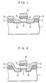
- an oxide film 3 made of SiO2 and having a thickness of about 10 nm is formed on the substrate 1 by thermal oxidation which is carried out in an atmosphere of oxygen kept at about 950°C.
- a poly-silicon layer (that is, first layer) 4 which will be used for forming a gate electrode, is deposited by the CVD (chemical vapor deposition) method to a thickness of about 100 nm, and a large amount of phosphorus is diffused into the first layer 4.
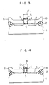
- an oxide film 3 made of SiO2 and having a thickness of about 10 nm is formed on the substrate 1 by thermal oxidation which is carried out in an atmosphere of oxygen kept at about 950°C.
- a poly silicon layer (that is, first layer) 4 is deposited by the CVD method to a thickness of about 100 nm, and a silicon nitride layer (that is, second layer) 5 is deposited on the poly-silicon layer 4 to a thickness of about 50 nm.
- a resist pattern made of a nega-type electron beam resist material is formed by the electron beam lithography.
- a silicon nitride layer 5 which acts as a mask when source and drain regions are formed through ion implantation techniques, is formed on the top of the gate electrode 4, and the side surface of the gate electrode 4 is covered with a silicon nitride film (that is, second insulating film) 7 for insulating the gate electrodes 4 from the source and drain electrodes 6. It is desirable to make the thickness of the second insulating film 7 as small as possible.
- the gate length of the present embodiment is equal to the sum of the width of the gate electrode 4 and the resultant thickness of the second insulating film 7 formed on both sides of the gate electrode, and hence the superconducting proximity effect can be enhanced by reducing the thickness of the second insulating film 7.
- the superconducting electrode layer 6 is made of niobium.
- the material of the layer 6 is not limited to niobium, but the layer 6 may be made of a superconducting alloy which has been already mentioned, an oxide superconducting material, or an organic superconducting material.
- the gate electrode 4 will be surely insulated from the superconducting electrodes.
- the insulating film 7 made of silicon nitride can be used even when the gate electrode is made very small in size.
- the insulating film 7 may be made of SiO2, SiO, Al2O3, YSZ (yttrium stabilized zirconia), MgO, or yttrium oxide. Further, the insulating film 7 may be formed of the self-oxidation film of the gate electrode.
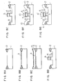
- Fig. 4 is a sectional view showing the fourth embodiment.
- a gate electrode 4 is interposed between first and second superconducting electrodes 6 corresponding to source and drain electrodes, in such a manner that a silicon nitride film (that is, second insulating film) 7 is sandwiched between the gate electrode 4 and the first or second superconducting electrode 6.
- the present embodiment is different from the third embodiment of Fig.
- a source region, the channel region and a drain region are formed at the same level, and hence the above superconducting current can flow efficiently.
- the distance between the source and drain electrodes is determined by the width of each of the protrusion 9 and the gate electrode 4, and is required to be less than ten times the coherence length in the substrate 1. Accordingly, in the present embodiment, the gate electrode 4 is made small in size, and the size surface of the gate electrode 4 is electrically from the source and drain electrodes.
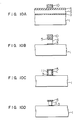
- a gate oxide film 3 made of SiO2 and having a thickness of about 10 nm is formed on the substrate 1 by thermal oxidation which is carried out in an atmosphere of pure oxygen kept at about 950° (Fig. 8B).
- a poly-silicon layer 4 is deposited by the CVD method to a thickness of about 100 nm, and a silicon nitride layer 5 is deposited on the poly-silicon layer 4 to a thickness of about 50 nm (Fig. 8C).
- a resist layer made of a nega-type electron beam resist material is formed by the electron beam lithography.
- the silicon nitride layer 5, the poly-silicon layer 4 and the gate oxide film 3 are etched in accordance with the above resist pattern used as a mask, by the reactive ion etching method using CF4 gas. Further, the substrate 1 is etched in accordance with the above resist pattern to a depth of about 100 nm (Fig. 8D). Next, the exposed surfaces of the substrate 1 and the poly-silicon layer 4 are oxidized by thermal oxidation which is carried out in an atmosphere of pure oxygen, so as to form an oxide film having a thickness of about 10 nm.
- a superconducting layer (that is, niobium layer) 6′ is left on the top of the silicon nitride layer 5.
- the gate electrode will surely be electrically isolated from the source and drain electrodes.
- the superconducting electrodes can be formed so as to be kept in contact with the insulating film on the side surface of the gate electrode, and hence the distance between the superconducting electrodes can be set to a desired value without generating the electrical breakdown between the gate electrode and the superconducting electrodes.
- the above distance is scarcely affected by conditions, under which the superconducting electrodes are formed.
- the present embodiment is excellent in reproducibility.
Landscapes
- Superconductor Devices And Manufacturing Methods Thereof (AREA)
- Junction Field-Effect Transistors (AREA)
Applications Claiming Priority (4)
| Application Number | Priority Date | Filing Date | Title |
|---|---|---|---|
| JP23670/88 | 1988-02-05 | ||
| JP63023670A JPH01200680A (ja) | 1988-02-05 | 1988-02-05 | 超電導電界効果トランジスタ |
| JP162511/88 | 1988-07-01 | ||
| JP63162511A JP2680046B2 (ja) | 1988-07-01 | 1988-07-01 | 超電導トランジスタおよびその製造方法 |
Publications (2)
| Publication Number | Publication Date |
|---|---|
| EP0327121A2 true EP0327121A2 (fr) | 1989-08-09 |
| EP0327121A3 EP0327121A3 (fr) | 1990-01-10 |
Family
ID=26361076
Family Applications (1)
| Application Number | Title | Priority Date | Filing Date |
|---|---|---|---|
| EP89101951A Withdrawn EP0327121A3 (fr) | 1988-02-05 | 1989-02-03 | Transistor à effet champ à supraconducteur |
Country Status (2)
| Country | Link |
|---|---|
| US (1) | US5317168A (fr) |
| EP (1) | EP0327121A3 (fr) |
Cited By (1)
| Publication number | Priority date | Publication date | Assignee | Title |
|---|---|---|---|---|
| US5521862A (en) * | 1990-12-21 | 1996-05-28 | Texas Instruments Incorporated | Apparatus and method for storing information in magnetic fields |
Families Citing this family (1)
| Publication number | Priority date | Publication date | Assignee | Title |
|---|---|---|---|---|
| US7615385B2 (en) | 2006-09-20 | 2009-11-10 | Hypres, Inc | Double-masking technique for increasing fabrication yield in superconducting electronics |
Family Cites Families (5)
| Publication number | Priority date | Publication date | Assignee | Title |
|---|---|---|---|---|
| EP0147482B1 (fr) * | 1983-12-28 | 1987-08-19 | International Business Machines Corporation | Transistor tunnel pour basses températures |
| EP0160456B1 (fr) * | 1984-04-19 | 1996-07-17 | Hitachi, Ltd. | Dispositif supraconducteur |
| EP0667645A1 (fr) * | 1984-11-05 | 1995-08-16 | Hitachi, Ltd. | Dispositif supraconducteur |
| JPS62131588A (ja) * | 1985-12-04 | 1987-06-13 | Hitachi Ltd | 超伝導トランジスタの製法 |
| US4837609A (en) * | 1987-09-09 | 1989-06-06 | American Telephone And Telegraph Company, At&T Bell Laboratories | Semiconductor devices having superconducting interconnects |
-
1989
- 1989-02-03 EP EP89101951A patent/EP0327121A3/fr not_active Withdrawn
-
1992
- 1992-11-19 US US07/978,454 patent/US5317168A/en not_active Expired - Fee Related
Cited By (1)
| Publication number | Priority date | Publication date | Assignee | Title |
|---|---|---|---|---|
| US5521862A (en) * | 1990-12-21 | 1996-05-28 | Texas Instruments Incorporated | Apparatus and method for storing information in magnetic fields |
Also Published As
| Publication number | Publication date |
|---|---|
| EP0327121A3 (fr) | 1990-01-10 |
| US5317168A (en) | 1994-05-31 |
Similar Documents
| Publication | Publication Date | Title |
|---|---|---|
| EP0181191B1 (fr) | Dispositif supraconducteur | |
| EP0070402B1 (fr) | Procédé pour former des configurations électroconductrices sur un dispositif semiconducteur, et un dispositif semiconducteur fabriqué par le procédé | |
| EP0478465A1 (fr) | Procédé de fabrication d'un dispositif supraconducteur ayant une couche d'oxyde supraconductrice à épaisseur réduite et dispositif à supraconducteur fabriqué ainsi | |
| EP0484253B1 (fr) | Dispositif supraconducteur ayant un canal extrêmement mince formé en matériau supraconducteur d'oxyde et méthode pour sa fabrication | |
| EP0095773B1 (fr) | Procédé de fabrication d'une barrière tunnel de Josephson | |
| US4425379A (en) | Polycrystalline silicon Schottky diode array | |
| US5717222A (en) | Superconducting device having an extremely thin superconducting channel formed of oxide superconductor material and method for manufacturing the same | |
| JPH05251777A (ja) | 超電導電界効果型素子およびその作製方法 | |
| US4544937A (en) | Formation of normal resistors by degenerate doping of substrates | |
| US5739084A (en) | Method for manufacturing a superconducting device having a reduced thickness of oxide superconducting layer | |
| US5446015A (en) | Superconducting device having a reduced thickness of oxide superconducting layer | |
| US4628339A (en) | Polycrystalline silicon Schottky diode array | |
| EP0577137B1 (fr) | Dispositif à effet quantique et procédé pour sa fabrication | |
| US5317168A (en) | Superconducting field effect transistor | |
| US5714767A (en) | Method for manufacturing superconducting device having a reduced thickness of oxide superconducting layer and superconducting device manufactured thereby | |
| US5304817A (en) | Superconductive circuit with film-layered josephson junction and process of fabrication thereof | |
| US4695856A (en) | Semiconductor device | |
| JPS62131588A (ja) | 超伝導トランジスタの製法 | |
| EP0487922B1 (fr) | Dispositif électronique de commutation à grande vitesse | |
| JP2738144B2 (ja) | 超電導素子および作製方法 | |
| JP2597745B2 (ja) | 超電導素子および作製方法 | |
| JP2641974B2 (ja) | 超電導素子および作製方法 | |
| JP2597747B2 (ja) | 超電導素子および作製方法 | |
| JP2680046B2 (ja) | 超電導トランジスタおよびその製造方法 | |
| JP2641975B2 (ja) | 超電導素子および作製方法 |
Legal Events
| Date | Code | Title | Description |
|---|---|---|---|
| PUAI | Public reference made under article 153(3) epc to a published international application that has entered the european phase |
Free format text: ORIGINAL CODE: 0009012 |
|
| AK | Designated contracting states |
Kind code of ref document: A2 Designated state(s): DE FR |
|
| PUAL | Search report despatched |
Free format text: ORIGINAL CODE: 0009013 |
|
| AK | Designated contracting states |
Kind code of ref document: A3 Designated state(s): DE FR |
|
| RHK1 | Main classification (correction) |
Ipc: H01L 39/22 |
|
| 17P | Request for examination filed |
Effective date: 19900629 |
|
| 17Q | First examination report despatched |
Effective date: 19930812 |
|
| STAA | Information on the status of an ep patent application or granted ep patent |
Free format text: STATUS: THE APPLICATION IS DEEMED TO BE WITHDRAWN |
|
| 18D | Application deemed to be withdrawn |
Effective date: 19940223 |