EP0667645A1 - Dispositif supraconducteur - Google Patents
Dispositif supraconducteur Download PDFInfo
- Publication number
- EP0667645A1 EP0667645A1 EP95104470A EP95104470A EP0667645A1 EP 0667645 A1 EP0667645 A1 EP 0667645A1 EP 95104470 A EP95104470 A EP 95104470A EP 95104470 A EP95104470 A EP 95104470A EP 0667645 A1 EP0667645 A1 EP 0667645A1
- Authority
- EP
- European Patent Office
- Prior art keywords
- superconducting
- semiconductor
- layer
- electrodes
- impurity concentration
- Prior art date
- Legal status (The legal status is an assumption and is not a legal conclusion. Google has not performed a legal analysis and makes no representation as to the accuracy of the status listed.)
- Withdrawn
Links
Images



Classifications
-
- H—ELECTRICITY
- H10—SEMICONDUCTOR DEVICES; ELECTRIC SOLID-STATE DEVICES NOT OTHERWISE PROVIDED FOR
- H10D—INORGANIC ELECTRIC SEMICONDUCTOR DEVICES
- H10D84/00—Integrated devices formed in or on semiconductor substrates that comprise only semiconducting layers, e.g. on Si wafers or on GaAs-on-Si wafers
- H10D84/01—Manufacture or treatment
-
- H—ELECTRICITY
- H10—SEMICONDUCTOR DEVICES; ELECTRIC SOLID-STATE DEVICES NOT OTHERWISE PROVIDED FOR
- H10D—INORGANIC ELECTRIC SEMICONDUCTOR DEVICES
- H10D86/00—Integrated devices formed in or on insulating or conducting substrates, e.g. formed in silicon-on-insulator [SOI] substrates or on stainless steel or glass substrates
- H10D86/01—Manufacture or treatment
-
- H—ELECTRICITY
- H10—SEMICONDUCTOR DEVICES; ELECTRIC SOLID-STATE DEVICES NOT OTHERWISE PROVIDED FOR
- H10N—ELECTRIC SOLID-STATE DEVICES NOT OTHERWISE PROVIDED FOR
- H10N60/00—Superconducting devices
- H10N60/10—Junction-based devices
- H10N60/128—Junction-based devices having three or more electrodes, e.g. transistor-like structures
Definitions
- the present invention relates to a cryogenic superconducting device designed to operate at extremely low temperatures and, more particularly, to a superconducting device for controlling the number of superconducting or normal conducting electrons, which tunnel through a semiconductor, by a voltage applied to a control electrode.
- this element In the conventional switching devices operative at extremely low temperatures, there is known a Josephson element. It has some advantages including a high switching speed and a small power consumption of several microwatts or so. However, this element is basically a two-terminal device, which is therefore not adapted for use in forming a circuit by the prior techniques accumulated in connection with the known semiconductor transistors, and employment of an AC power supply is requisite.
- a superconducting device has been developed by means of combining a superconductor and a semiconductor, as disclosed in Japanese Patent Laid-open No. 57-106186.
- a pair of superconducting layers are deposited on a semiconductor substrate with the respective end faces opposed to each other, and a control conductor is disposed in such opposed portions through an insulator layer.
- a superconducting layer formed on the semiconductor substrate is separated into two superconducting electrodes by photolithography and etching. Subsequently the portion thus separated is thermally oxidized to form an insulator film, and then a desired control electrode is formed by evaporation.
- JOFET Hybrid Josephson Field Effect Transistors
- T. D. Clark As reported in J. Appl. Phys., vol. 51, pp. 2736 - 2745, 1980.
- an electrode of a superconductor is formed on a semiconductor substrate doped to a high concentration, or a dope layer is formed on a high-purity buffer layer and an electrode of a superconductor is formed thereon.
- control of its characteristics is executed by applying a voltage to the control electrode and extending the inversion layer from the control electrode side toward the semiconductor side.
- the superconducting device of the present invention is suitable for high-density integration.
- the present invention may also make it possible to provide a superconducting device in which the parasitic capacity is reducible to enable a high speed operation.
- the present invention may provide a superconducting device which retains a great gain in controlling the coupling state between superconducting electrodes by an applied voltage.
- the superconducting device of the present invention is constituted as follows. 1) A pair of superconducting electrodes are formed on two sides of a semiconductor, and a control electrode is disposed on the semiconductor through an insulator film so as to control a superconductive weak coupling state in the semiconductor between the superconducting electrodes.
- the distance between the superconducting electrodes should be less than 10 times the coherent length ⁇ n of an electron pair.
- the manufacturing precision can be enhanced by determining the interelectrode distance in accordance with the thickness of the semiconductor interposed between the superconducting electrodes, whereby the uniformity of the device characteristics can be improved as well.
- Determination of the interelectrode distance in accordance with the semiconductor thickness is achieved by first etching a semiconductor substrate to form a, projection thereon and then disposing a pair of superconducting electrodes on the two sides of such projection. According to this process, the accuracy of the spatial distance between the superconducting electrodes is dependent on the precision of the semiconductor substrate. Therefore a high manufacturing precision is attainable regardless of any other condition such as the hardness of the superconductor material. It is desired that the height of the projection be equivalent to at least the thickness of the superconducting electrode.
- the electrode for controlling the superconductive weak coupling state is formed in an upper or lower portion of the semiconductor projection through an insulator film. It is a matter of course that the control electrode may be provided in each of upper and lower portions.
- the superconducting device of such structure furnished with a control electrode particularly in an upper portion of the projection is of a planar type adapted for realizing an arrangement of high-density integration.
- Reduction of a parasitic capacity is achievable by shaping a channel-defining semiconductor into an insular contour. That is, first an insular semiconductor is formed on one side of the insulator film, then superconducting electrodes are formed in such a manner as to interpose the semiconductor therebetween, and subsequently a control electrode is formed on the other side of the insulator film.
- the above procedure eliminates the substrate capacity to eventually accomplish a satisfactory superconducting device which is capable of performing a high speed operation.
- the superconducting device of such structure can be shaped into a planar type with facility so that high-density integration thereof is rendered possible.
- At least two superconducting electrodes are disposed adjacent each other on a semiconductor layer (or substrate), and at least one,control electrode is formed for controlling current flow between the superconducting electrodes to change the interelectrode superconductive weak coupling.
- the distribution of inpurities contained in the semiconductor layer is so arranged as to include at least one region of a high impurity concentration above the average and at least one region of a low impurity concentration below the average. Due to such varied concentration distribution of impurities contained in the semiconductor layer that serves as the superconducting electrode, the gain is increasable in controlling the interelectrode coupling state by an applied voltage.
- the semiconductor layer in the conventional superconducting device contains impurities uniformly at a high concentration, attainable extension of a charge storage layer or inversion layer is relatively small in comparison with the voltage applied to the control electrode.
- the extension of the charge storage layer or inversion layer is caused in a different manner as compared with that induced in a uniform distribution of impurities, so that application of a lower voltage is sufficient to extend the charge storage layer or inversion layer with facility, hence increasing the gain.
- the impurity concentration in a semiconductor region proximate to the control electrode is made to be high while the impurity concentration in other semiconductor regions proximate to the superconducting electrodes is made to be low in such a manner that the concentration distribution is formed in the direction of depth of the semiconductor layer.
- the charge storage layer is extendable readily from the high concentration layer toward the low concentration layer by the application of a low control voltage.
- the superconductive weak coupling state can be changed with facility by a low control voltage to eventually bring about an effect of increasing the gain.
- the inversion layer its extension is not induced easily until the control voltage exceeds a given value (i.e. until the inversion layer extends to the high impurity concentration layer), but upon rise of the voltage to cause extension of the inversion layer to the low impurity concentration layer, desired extension is induced readily even with a subsequent slight rise of the voltage. Consequently, utilization of such characteristic phenomenon realizes a satisfactory superconducting device of a great gain in which the characteristic thereof remains substantially unchanged until arrival of the control voltage at a certain fixed value but is sharply changed upon subsequent excess of the control voltage over the fixed value.
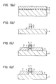
- Fig. 1 (c) is a sectional view of a superconducting transistor structure according to the present invention, wherein a projection 4 is formed in a portion of a semiconductor substrate 1, and a pair of mutually opposed superconducting electrodes 2 and 3 are disposed on the two sides of the projection 4. And a control electrode 5 with insulated lateral surfaces is disposed on the projection 4 through an insulator layer 6.
- the superconducting electrodes 2 and 3 are composed of a semiconductor such as silicon, a narrow gap of 0.2 microns is kept there- between.
- Superconducting electron pairs are emitted from the superconducting electrodes 2 and 3 onto the semiconductor substrate 1 or the projection 4 thereof and then are advanced to flow in the semiconductor interposed between the superconducting electrodes. Such flow of the superconducting electron pairs is controllable by a voltage applied to the control electrode 5.
- the superconducting electrodes 2 and 3 are coupled to each other by superconductive weak interaction when cooled below the transition temperature of the superconducting electrode material, and the maximum Josephson current 1m flowing between the two superconducting electrodes due to such coupling is given by where A is gap energy of the superconducting electrodes 2 and 3; e is an elementary charge; and R N is a normalconduction tunnel resistance in the superconductive weak coupling.
- A is gap energy of the superconducting electrodes 2 and 3
- e is an elementary charge
- R N is a normalconduction tunnel resistance in the superconductive weak coupling.
- a substrate 1 composed of monocrystal silicon is oxidized for an hour in a steam- containing oxygen atmosphere at 1200 ° C to form thereon an insulator layer 6 of Si0 2 having a thickness of 80 nanometers, and then a control electrode 5 of polycrystal silicon is formed to a thickness of 0.3 microns by electron beam evaporation in a high vacuum receptacle, as shown in Fig. 1 (a).
- a control electrode 5 of polycrystal silicon is formed to a thickness of 0.3 microns by electron beam evaporation in a high vacuum receptacle, as shown in Fig. 1 (a).
- plasma etching is executed with CF 4 gas to a portion of the substrate 1, as shown in Fig. 1 (b).
- superconducting electrodes 2 and 3 composed of Pb and having a thickness of 300 nanometers are formed by resistance heating evaporation and lift-off.
- the superconducting electrodes may be formed in contact with a projection 4 as shown in Fig. 1 (c) or may be formed separately therefrom as shown in Fig. 1 (d).
- the lateral surface of the control electrode 5 is thermally oxidized to form an insulator layer 7 thereon.
- a material suitable for such insulator layers 6 and 7 may be selected from SiO, SiaN 4 and A1 2 0 3 in addition to the aforesaid Si0 2 .
- the semiconductor its material may be Si or Ge containing an impurity such as P, B or As at a concentration higher than 10 19 cm- 3 ; or GaAs, InAs or InP containing an impurity such as Si, Zn or Ge at a concentration higher than 10 17 cm- 3 .
- the control electrode 4 may be composed of Ti, W, Mo, Poly-Si, Al, Cu or Pt as well.
- a material for the superconducting electrodes 2 and 3 may be Pb or Pb-based alloy (e.g. Pb-Au, Pb-In, Pb-Au-In or Pb-Bi); or Nb or its compound (e.g. NbN, Nb 3 AI, Nb 3 Ge or Nb 3 Sn).
- Pb or Pb-based alloy e.g. Pb-Au, Pb-In, Pb-Au-In or Pb-Bi
- Nb or its compound e.g. NbN, Nb 3 AI, Nb 3 Ge or Nb 3 Sn.
- the projection 4 serving as a channel layer can be easily formed with a high accuracy to have a dimension (approx, 0.5 microns or less although different depending on the semiconductor material, impurity concentration and other condition) which is about 10 times the coherent length of the superconductor.
- any malfunction is preventable in this exemplary embodiment where the insulator layer 7 is formed around the control electrode 4 to ensure interelectrode separation.
- a self-align process is applicable to eventually reduce the number of masks and that of steps required, hence facilitating the manufacture in view of the process.
- a control electrode 25 composed of niobium and having a thickness of 200 nanometers and a width of 10 microns is formed on a substrate 21 of monocrystal silicon which is covered with an oxide film 28 of 0.7 microns in thickness, and the surface of the control electrode 25 is oxidized to form an insulator film 26 thereon.
- a semiconductor layer 24 composed of polycrystal or amorphous silicon and having a thickness of 300 nanometers is formed by electron beam evaporation in a high vacuum receptacle, and the semiconductor 24 is etched partially or entirely by the same method as employed for the first embodiment with an electron beam resist used as a mask.
- the etching be executed in a depth equivalent to at least the thickness of superconducting electrodes 22 and 23 which are to be formed in the next step.
- the superconductor layer is composed of niobium and measures 200 nanometers in thickness.
- a fast-etchable material such as niobium or a compound thereof
- the precision of the spatial distance between the two superconducting electrodes is determined regardless of the superconductor material and merely by the manufacturing precision of the semiconductor substrate, hence not dependent on any ther condition such as the hardness of the superconductor material. Consequently, even when the superconductor material is changed from Pb alloy to Nb or its compound, high-precision processing can be performed to ensure remarkable uniformity in the device characteristic, whereby a high yield rate is attainable in manufacture.
- a thin film 32 of niobium is deposited to a thickness of 300 microns on a substrate 31 by DC magnetron sputtering, a channel layer 34 composed of silicon and having a thickness of 200 nanometers is formed thereon by vapor-phase growth or molecular beam growth, and boron is introduced as an impurity at a concentration of 10 25 cm- 3 by ion implantation. Then a thin film 33 of niobium having a thickness of 300 nanometers is deposited again to constitute a laminated structure, which is subsequently processed by ion etching with a photoresist used as a mask to obtain a desired shape.
- the surface of the lateral wall is thermally oxidized for 10 minutes in an oxygen atmosphere at 1000°C, thereby forming an insulator film 36 of about 20 nanometers in thickness.
- niobium is deposited to a thickness of 800 nanometers by DC magnetron sputtering.
- reactive ion etching is executed with CF 4 gas in such a manner as to leave niobium of 2 microns in width on the right side of the thermally oxidized film, whereby a third electrode 35 is obtained.
- the superconducting transistor of this embodiment shown in Fig. 11 is thus manufactured by the above procedure.
- the thickness of the semiconductor is utilized to determine the distance between the superconducting electrodes
- accurate control can be performed to minimize variation in the transistor characteristic as well as to raise the yield rate in manufacture.
- an interlayer insulator film is not necessary to bring about an advantageous effect of facilitating the production steps.
- a composite device can be constituted with facility by connecting a plurality of such superconducting transistors in series to obtain a greater output amplitude.
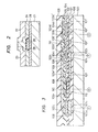
- Fig. 3 is a sectional view of a superconducting integrated circuit which is a third embodiment of the present invention.
- component elements including a superconducting device T, a diffused resistor D, a metal thin film resistor R and an electrostatic capacitor C are integrated on a single substrate.
- this integrated circuit is constituted of thin film structure which comprises a substrate 100 for mounting component elements thereon, a metal film 101 or a semiconductor film containing an impurity introduced therein and serving as a wiring layer, an insulator film 102 formed on the metal film 101, a superconducting metal 103 located on the insulator film 102, and an insular semiconductor thin film 104.
- a material for the substrate 100 is selected from an inorganic substance such as monocrystal or polycrystal silicon and an organic substance such as resin.
- the metal film 101 is composed of a stable material such as AI or Au, or a superconducting metal.
- the insulator film 102 is composed of an insulating substance such as resin or silicon compound typically represented by silicon oxide (e.g. Si0 2 or SiO) or silicon nitride.
- the superconducting metal 103 a Pb-based or Nb-based metal is used.
- the semiconductor thin film 104 is usually composed of Si, Ge, GaP, GaAs, GaSb, InP, InAs or InSb.
- any of such substances be a monocrystal, but polycrytal or amorphous one is usable as well.
- An impurity is contained in this semiconductor thin film at a concentration of 10 19 to 10 20 cm- 3 .
- an impurity typically used is B, P or As.
- a gate insulator film 102t is formed in a thin Portion obtained by selectively reducing the thickness of an insulator film 102, and a metal film 101 proximate to the substrate 100 is processed to serve as a gate electrode 101t.
- An insular semiconductor thin film 104 on the gate insulator film 102t is formed into a channel layer 104t, and a superconducting metal 103 so shaped as to cover the semiconductor thin film 104t while holding it from two sides is processed to become superconducting electrodes 103t and 103t' which are spaced apart from each other by a narrow gap of 0.2 microns or so.
- the gate electrode 101t is connected to a metal film 103r' formed on the insulator film 102 via a through-hole 107 in the insulator film 102 and is thereby connected to other component elements.
- the superconducting electrodes 103t and 103t' are connected respectively to metal films 110 and 111 which are formed on the insulator film 108 via through-holes 109 and 109' in the insulator film 108 located on both the superconducting metal 103 and the semiconductor thin film 104, whereby the superconducting electrodes 103t and 103t' are connected to other component elements.
- the superconducting device T thus constituted with a semiconductor thin film furnished separately from the substrate to serve as a channel layer is of a planar structure adapted for high-density integration and easily integrable with other elements as well.
- the fiffused resistor D integrated on the substrate together with the superconducting device T comprises a semiconductor thin film 104d formed on the insulator film 102 and metal films 103d and 103d' which serve as electrode films connected to the two ends of the semiconductor thin film 104d, wherein the metal film 103d is connected also to the superconducting electrode 103t'.
- the metal thin film resistor R is so formed that metal films 103r and 103r' serving as electrode films are connected to two ends of the metal resistor thin film 112.
- a material suitable for the metal resistor thin film is a normal conducting metal such as a compound or alloy of Au, Ag, Mo, Cr, Al, Ta, Nb or W.
- the electrostatic capacitor C is constituted by forming metal films 103c and 101c as electrodes above and below a portion 102c obtained by selectively reducing the thickness of the insulator film 102.
- the metal film 101' is used for wiring.
- the above-mentioned substrate 100, metal film 101, insulator film 102, superconducting metal film 103 and insular semiconductor thin film 104 function as basic elements to constitute a superconducting integrated circuit, whereby the entire components including the superconducting device can be arranged on the surface of the substrate, hence realizing high-density integration.
- this embodiment since this embodiment has an ideal structure where the entire components are embedded in the insulator film, the parasitic capacity can be reduced to eventually bring about another advantage of fast device operation.
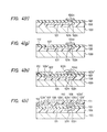
- an oxide layer serving as an insulator film 102 is formed on a substrate 200 of monocrystal silicon and is selectively thinned to shape a portion corresponding to a gate insulator film 102t.
- This film is producible by thermally oxidizing the surface of the monocrystal silicon to form a thick oxide film, then etching such oxide film selectively, and subsequently processing it to a thin oxide film to obtain a desired film structure.
- the insulator film 102 is shaped to have a thickness of 2000 angstroms, and the gate insulator film is shaped to have a thickness of 200 angstroms [Fig. 4 (a)].
- boron is introduced by ion implantation so as to be contained at a concentration of 10 19 cm- 3 , whereby a channel layer 104' is formed to serve as an insular semiconductor thin film 104 [Fig. 4 (b)].
- a metal film 101 is formed to a thickness of 3000 angstroms, thereby producing a gate electrode 101t [Fig. 4 (c)].
- an insulator film 106 and a substrate 100 are superposed thereon in a laminated structure.
- the substrate 100 is dimensionally so selected as to have a thickness of 200 microns or so (Fig. 4 (d)].
- the substrate 200 of monocrystal silicon is processed by etching from its reverse side in such a manner that merely the regions of a low impurity concentration are etched by utilizing the anisotropic etching property of silicon, whereby only a channel layer 104' of a high impurity concentration can he left.
- the channel layer 104' is processed to have a thickness of 1000 angstroms by the aforesaid ion implantation and the above etching. It is to be noted here that, in this stage of production, the channel layer 104' is on the obverse side [Fig.
- the channel layer 104' is processed by selective etching to form a portion corresponding to a channel layer 104t of the superconducting device T [Fig. 4 (f)].
- the insulator film 102 is selectively etched to form a through-hole 107, and further a metal resistance thin film 112 is formed [Fig. 4 (g)].
- a metal film of 3000 angstroms in thickness is formed to produce a metal film 103r' which is connected to the gate electrode 102t, and also superconducting electrodes 103t and 103t'.
- the gap between these two electrodes 103t and 103t' is established to be 200 nanometers [Fig. 4 (h)].
- an insulator film 108 is produced with through-holes 109 and 109' formed selectively.
- metal films 110 and 111 are formed in connection to the superconducting electrodes 103t and 103t', respectively. Desired shapes thereof are obtained by the art of liftoff and etching [Fig. 4 (i)].
- a protection film 105 is formed to finish constituting the superconducting device T which is a fundamental component of the superconducting integrated circuit shown in Fig. 1. It is to be understood that the steps illustrated in Fig. 4 are typical examples, and the superconducting integrated circuit of Fig. 3 can also be manufactured by altering the sequence of such steps or by employment of some other method.
- the channel layer 104' can be formed by executing the ion implantation of Fig. 4 (b) prior to forming the insulator film 102 of Fig. 4 (a).
- the ion implantation may be selectively executed in Fig. 4 (b), and an insular film of monocrystal silicon corresponding to the channel layer 104t is formable directly when the substrate 200 of monocrystal silicon is etched in Fig. 4 (e).
- the art of MBE or laser annealing may be applied to formation of the channel layer 104t.
- a superconducting device is constituted by first forming electrodes 52 and 53 of a superconductor on either a substrate 51, which becomes an insulator at extremely low temperatures, or an insulator film 58 provided previously on the substrate 51, then forming a semiconductor layer 54 on the electrodes 52 and 53, further forming an insulator layer 56 thereon, and finally forming a control electrode 55 on the insulator layer.
- the semiconductor layer where a superconducting or normal conducting current flows, is electrically isolated from the substrate so that no substrate capacity is existent therein. Accordingly it becomes possible to increase the switching speed in the circuit operation. Since a high resistance material is usable for the substrate, the necessity of providing particular means to separate the components from one another can be eliminated when arraying a multiplicity of superconducting devices on the substrate
- a heat treatment is effective for improving the crystalline and electrical properties of the semiconductor layer.
- deterioration may be induced in the superconductivity of the superconductor located under the semiconductor layer.
- it has been confirmed that such deterioration in the characteristic of the superconductor under the semiconductor layer is preventable despite a heat treatment of the semiconductor layer if any of NbN, Nb 3 Si, Nb 3 Ge, MoN and V 3 Si is used as a material for the superconductor.
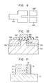
- a sixth embodiment of the present invention is shown in Fig. 6. Boron is introduced into a substrate 61 of monocrystal silicon in the [100] direction thereof by ion implantation with application of an acceleration voltage of 70 KeV to attain an impurity concentration of 10 15 cm- 3 , and then the substrate 61 is annealed for 35 minutes in a nitrogen atmosphere at 900 °C. This treatment produces a high impurity concentration layer 62 having a thickness of about 200 nanometers. Aster cleaning the surface thereof, a low impurity concentration layer 63 is formed thereon by molecular beam epitaxy or vapor-phase growth in such a manner that boron is contained as an impurity at a concentration of 10 16 -10 18 cm- 3 .
- the amount of the boron impurity to be contained in the low impurity concentration layer 63 is so selected as to become smaller than the amount in the high impurity concentration layer 62.
- the impurity concentration be about 1011 to 1016 cm-3 in the low concentration layer, or about 10 16 to 10 19 cm- 3 in the high concentration layer.
- the substrate 61 of monocrystal silicon is etched from its reverse side by the use of a chemical such as KOH with a mask of SiC 2 or the like formed by vapor-phase growth at a normal pressure. Since the etching speed on the [100] face of the monocrystal silicon is higher than that on the [111] face in this process, the shape obtained becomes such as shown in Fig. 6. Subsequently the surface of the monocrystal silicon substrate 61 is oxidized in a pure oxygen atmosphere at 1000 ° C to form an oxide layer 64 of Si0 2 having a thickness of about 40 nanometers. Then aluminum is deposited thereon by resistance heating evaporation to a thickness of about 500 nanometers, thereby producing a control electrode 65.
- an oxide film of silicon also grows on the surface of the low impurity concentration layer 63. Therefore, such oxide film is removed by chemical etching to clean the surface of the low impurity concentration layer 63. Then niobium is deposited by DC magnetron sputtering to a thickness of 300 nanometers on the surface of the low impurity concentration layer 63 thus cleaned, and the niobium film is processed by reactive ion etching while being masked with a pattern of an electron beam resist having a thickness of 350 nanometers, thereby producing first and second superconducting electrodes 66 and 67.
- the distance between such first and second superconducting electrodes be less than 0.2 microns.
- the procedure mentioned above completes a superconducting device of the present invention.
- the device thus produced is cooled to the temperature of liquid helium and placed in operation.
- a negative voltage is applied to the control electrode, a positive- charge storage layer extends readily into the low impurity concentration layer 63.
- the superconductive coupling state between the first and second superconducting electrodes 66 and 67 can be changed by a control signal of a low voltage such as 10 mV or so, whereby the gain is increased 2.5 to 3 times as compared with the value obtained in a uniform impurity distribution.
- the superconducting device has a given threshold value (not zero) for starting the operation as compared with the case of a uniform impurity distribution and still is furnished with a remarkable function of ensuring a great gain.
- the high impurity concentration layer is formed proximate to the control electrode while the low impurity concentration layer proximate to the superconducting electrodes, it is permitted to reverse the positional relationship in such a manner that the low impurity concentration layer is formed proximate to the control electrode while the high impurity concentration layer proximate to the superconducting electrodes.
- a charge inversion layer or a charge storage layer extends readily into the low impurity concentration layer in response to a low control voltage, whereby the gain is rendered great.
- This modification has such a feature that when the applied voltage rises above a certain given value, the inversion layer or storage layer comes to extend into the high impurity concentration layer, so that further extension of the invertion layer or storage layer is hardly induced to eventually diminish the device characteristic variation.
- the impurity concentration is high on the side proximate to the superconducting electrodes, another effect is produced that both the height and width of the Schottky barrier existing in the interface between the semiconductor and the superconductor are reduced to facilitate emission of electrons from the superconducting electrodes into the semiconductor.
- the spatial distance between the first and second superconducting electrodes is allowed to be longer than the conventional one, hence facilitating manufacture of the device.
- a seventh embodiment of the present invention is shown in Fig. 7, wherein a region of a low impurity concentration is located at the center of a semiconductor layer.
- a high impurity concentration layer 63' is formed by molecular beam epitaxy or the like on a low impurity concentration layer 62 formed similarly to the aforesaid one in the embodiment of Fig. 6.
- the seventh embodiment has a combination of the advantageous effects described in connection with the foregoing two structures (one example furnished with a high impurity concentration layer proximate to the control electrode and a low impurity concentration layer proximate to the superconducting electrodes; and another example having a reverse positional relationship thereof), whereby the gain is increased to facilitate manufacture of the device.
- FIG. 8 An eighth embodiment of the present invention is shown in Fig. 8, wherein a control electrode is disposed on the same side as the surface of a semiconductor layer on which superconducting electrodes are formed.
- a silicon substrate 301 containing phosphorus as an impurity at a concentration of 10 12 cm- 3 there are sequentially formed by molecular beam epitaxy a low impurity concentration layer 302 containing phosphorus at 10 13 cm- 3 , a low impurity concentration layer 303 containing phosphorus at 10 15 cm- 3 , and a low impurity concentration layer 302' containing phosphorus at 10 13 cm- 3 .
- an oxide layer of Si0 2 is formed thereon at a temperature of 500 °C and, after it is shaped into a pattern, phosphorus is introduced by ion implantation with the pattern used as a mask. Then niobium is deposited on the phosphorus-diffused surface by sputtering to a thickness of about 200 nanometers, and the Si0 2 layer used as a mask is removed by etching, whereby superconducting electrodes 306 and 307 are formed.
- an oxide film 304 of Si0 2 is formed by oxidation with 0 2 plasma, and finally a control electrode 305 is formed by evaporation of aluminum to a thickness of 500 nanometers.
- a storage layer or an inversion layer readily extends into the low impurity concentration layer 302' in response to a voltage applied to the control electrode 305, so that the gain can be increased exactly as in the foregoing embodiments.
- a low or high impurity concentration region may be formed in a limited portion of the semiconductor layer.
- the aimed effect is attainable if a high or low impurity concentration region is limited merely to a range including a portion immediately below each of the superconducting electrodes.
- the same effect is also obtainable if the impurity concentration difference is changed gradually, not stepwise.
- the semiconductor layer may he shaped insular with an impurity diffused therein in a desired distribution.
- the object of the present invention can be accomplished by the use of amorphous or polycrystal silicon as well.
- Silicon may be replaced with some other suitable substance such as Ge, GaAs, InAs, InP or InSb.
- the aforesaid Nb is replaceable with Pb or Pb-based alloy; Nb compound such as NbN, Nb 3 Sn, Nb 3 AI or Nb 3 Ge; or Mo compound such as MoN to attain the aimed effect.
- the material for the control electrode is not limited to AI alone, and a superconductor metal such as Pb offers the same effect.
- a Schottky barrier may be formed as well.
- a tenth embodiment of the superconducting device has such a feature that, for the purpose of realizing a planar structure and increasing the gain, two impurity introduced regions are formed on a semiconductor substrate to reduce the Schottky barrier, and a low impurity concentration region is formed there- between in such a manner as to be disposed in a projection of a height which is equivalent to or smaller than the thickness of superconducting electrodes formed on the semiconductor.
- Fig. 10 is a sectional view showing principal portions of the tenth exemplary superconducting device embodying the present invention.
- the surface of a silicon substrate 501 containing boron as an impurity at a concentration of 1 x 10 14 cm- 3 or less is oxidized to form thereon an oxide film 502 of Si0 2 to a thickness of 30 nanometers and, after a photoresist pattern is formed thereon to be used as a mask, the surface of the silicon substrate is processed by plasma etching with CF 4 gas or by ion beam etching with Ar or CF 4 gas, thereby forming a projection 503.
- the height of the projection 503, which corresponds to the amount of the silicon substrate removed by etching, should be equivalent to or smaller than the thickness of saperconducting electrodes to be formed later.
- such height is selected to be 200 nanometers.
- a sesirable width of the projection 503 ranges from 0.3 to 0.1 micron.
- boron is diffused throughout the entire surface of the sample at a surface con- cen t ra ti o n of 1 x 10 19 cm- 3 to form a diffusion layer 504.
- the process of diffusion may be replaced with ion implantation in forming the layer 504 to accomplish the object of this embodiment.
- An exemplary thickness of the diffusion layer is selected to be 50 nanometers from the surface.
- niobium is evaporated by electron beam heating in a high vacuum receptacle at 1 x 10- 6 Pa or less, whereby a niobium film is deposited to a thickness of about 200 nanometers.
- sputtering is also applicable in place of electron beam evaporation.
- the niobium film is processed by plasma etching with CF 4 gas to produce superconducting electrodes 505 and 506.
- the projection 503 and the superconducting electrodes 505 and 506 are existent substantially at the same height to realize the aim of flattening the device to a planar structure.
- an oxide film of Si0 2 is formed by vapor phase growth to a thickness of 50 nanometers and then is processed by plasma etching to form an insulator film 507.
- a niobium film is formed by vacuum evaporation and is processed by plasma etching to produce a control electrode 508, hence completing the superconducting device of the present invention.
- the aforesaid vapor phase growth is replaceable with sputtering.
- An integrated circuit manufactured by the use of such superconducting device is cooled to the temperature (4.2 K) of liquid helium and is placed in operation. Then emission of superconducting electrons into the semiconductor is expedited due to that the impurity concentration in a region corresponding to the channel is as low as 1 x 10 14 cm- 3 in this superconducting device and also that the diffusion layer is existent in a portion of the semiconductor adjacent to the superconductor. And the coherent length in the semiconductor is changed by a voltage of several millivolts applied to the control electrode, whereby the current flowing between the two superconducting electrodes is variable 10 to 100 times.
- the device is planar in shape as mentioned, wiring on the control electrode and lead layers for connection thereof can be arrayed in a multi-layer arrangement three-dimensionally to realize high density integration and an enhanced yield rate in manufacture.
- the interface level can be lowered to stabilize the device operation.
- silicon used for the semiconductor is replaceable with some other suitable substance such as GaAs, InAs, InP or InSb
- niobium used for the superconducting electrodes is replaced with Pb alloy; Nb compound such as NbN, Nb 3 Si, Nb 3 AI or Nb 3 Sn; or Mo compound such as MoN.
- boron may be replaced with phosphorus, arsenic or antimony.
- an impurity of the same conduction type is also usable to attain the aimed effect of the invention.
Landscapes
- Superconductor Devices And Manufacturing Methods Thereof (AREA)
Applications Claiming Priority (11)
| Application Number | Priority Date | Filing Date | Title |
|---|---|---|---|
| JP59231308A JPS61110479A (ja) | 1984-11-05 | 1984-11-05 | 超電導トランジスタの構造 |
| JP231308/84 | 1984-11-05 | ||
| JP60030366A JP2568995B2 (ja) | 1985-02-20 | 1985-02-20 | 超電導素子 |
| JP30366/85 | 1985-02-20 | ||
| JP34355/85 | 1985-02-25 | ||
| JP60034355A JPS61194884A (ja) | 1985-02-25 | 1985-02-25 | 超電導素子集積回路 |
| JP46539/85 | 1985-03-11 | ||
| JP60046539A JPS61206277A (ja) | 1985-03-11 | 1985-03-11 | 超電導トランジスタ |
| JP110371/85 | 1985-05-24 | ||
| JP60110371A JPS61269385A (ja) | 1985-05-24 | 1985-05-24 | 超伝導デバイス |
| EP85308009A EP0181191B1 (fr) | 1984-11-05 | 1985-11-04 | Dispositif supraconducteur |
Related Parent Applications (1)
| Application Number | Title | Priority Date | Filing Date |
|---|---|---|---|
| EP85308009.1 Division | 1985-11-04 |
Publications (1)
| Publication Number | Publication Date |
|---|---|
| EP0667645A1 true EP0667645A1 (fr) | 1995-08-16 |
Family
ID=27521216
Family Applications (2)
| Application Number | Title | Priority Date | Filing Date |
|---|---|---|---|
| EP95104470A Withdrawn EP0667645A1 (fr) | 1984-11-05 | 1985-11-04 | Dispositif supraconducteur |
| EP85308009A Expired - Lifetime EP0181191B1 (fr) | 1984-11-05 | 1985-11-04 | Dispositif supraconducteur |
Family Applications After (1)
| Application Number | Title | Priority Date | Filing Date |
|---|---|---|---|
| EP85308009A Expired - Lifetime EP0181191B1 (fr) | 1984-11-05 | 1985-11-04 | Dispositif supraconducteur |
Country Status (3)
| Country | Link |
|---|---|
| US (4) | US4884111A (fr) |
| EP (2) | EP0667645A1 (fr) |
| DE (1) | DE3588086T2 (fr) |
Families Citing this family (26)
| Publication number | Priority date | Publication date | Assignee | Title |
|---|---|---|---|---|
| EP0667645A1 (fr) * | 1984-11-05 | 1995-08-16 | Hitachi, Ltd. | Dispositif supraconducteur |
| US5272358A (en) * | 1986-08-13 | 1993-12-21 | Hitachi, Ltd. | Superconducting device |
| EP0257474A3 (fr) * | 1986-08-13 | 1989-02-15 | Hitachi, Ltd. | Dispositif supraconducteur |
| KR910002311B1 (ko) * | 1987-02-27 | 1991-04-11 | 가부시기가이샤 히다찌세이사꾸쇼 | 초전도 디바이스 |
| CN1014382B (zh) * | 1987-08-24 | 1991-10-16 | 株式会社半导体能源研究所 | 采用超导材料的电子器件 |
| EP0327121A3 (fr) * | 1988-02-05 | 1990-01-10 | Hitachi, Ltd. | Transistor à effet champ à supraconducteur |
| JPH07109906B2 (ja) * | 1988-03-03 | 1995-11-22 | 松下電器産業株式会社 | 超伝導トランジスタ回路 |
| JPH0298979A (ja) * | 1988-10-05 | 1990-04-11 | Sharp Corp | 超電導装置 |
| FR2638569B1 (fr) * | 1988-10-25 | 1992-11-20 | Seiko Epson Corp | Transistor josephson du type a effet de champ et procede de fabrication d'une jonction josephson |
| JPH02141569A (ja) * | 1988-11-24 | 1990-05-30 | Hitachi Ltd | 超伝導材料 |
| US5550389A (en) * | 1988-11-28 | 1996-08-27 | Hitachi, Ltd. | Superconducting device |
| FR2674067B1 (fr) * | 1991-03-15 | 1993-05-28 | Thomson Csf | Dispositif semiconducteur a effet josephson. |
| US5686317A (en) * | 1991-06-04 | 1997-11-11 | Micron Technology, Inc. | Method for forming an interconnect having a penetration limited contact structure for establishing a temporary electrical connection with a semiconductor die |
| JP2773487B2 (ja) * | 1991-10-15 | 1998-07-09 | 日本電気株式会社 | トンネルトランジスタ |
| US5250454A (en) * | 1992-12-10 | 1993-10-05 | Allied Signal Inc. | Method for forming thickened source/drain contact regions for field effect transistors |
| DE59504020D1 (de) * | 1994-11-22 | 1998-11-26 | Amo Gmbh | Tunnel-effekt bauelement und verfahren zu seiner herstellung |
| US5908813A (en) * | 1997-02-14 | 1999-06-01 | Micron Technology, Inc. | Method making integrated circuit metallization with superconductor BEOL wiring |
| US5930165A (en) * | 1997-10-31 | 1999-07-27 | The United States Of America As Represented By The Secretary Of The Navy | Fringe field superconducting system |
| DE19930531C2 (de) * | 1999-07-01 | 2001-07-05 | Infineon Technologies Ag | Tunnelkontakt und Verfahren zu seiner Herstellung |
| JP4194237B2 (ja) | 1999-12-28 | 2008-12-10 | 株式会社リコー | 電界効果トランジスタを用いた電圧発生回路及び基準電圧源回路 |
| US20060289976A1 (en) * | 2005-06-23 | 2006-12-28 | Intel Corporation | Pre-patterned thin film capacitor and method for embedding same in a package substrate |
| US7615385B2 (en) | 2006-09-20 | 2009-11-10 | Hypres, Inc | Double-masking technique for increasing fabrication yield in superconducting electronics |
| US7880204B2 (en) * | 2006-10-02 | 2011-02-01 | Massachusetts Institute Of Technology | System and method for providing a high frequency response silicon photodetector |
| EP3031443A1 (fr) | 2014-12-12 | 2016-06-15 | Basf Se | Composition comprenant de l'ester partiel d'hydrate de carbone |
| CN110335939B (zh) * | 2018-05-17 | 2021-05-04 | 大连理工大学 | 氟化异质结势垒层的半导体磁场传感器 |
| US12082512B2 (en) | 2019-10-24 | 2024-09-03 | Microsoft Technology Licensing, Llc | Semiconductor-superconductor hybrid device |
Citations (2)
| Publication number | Priority date | Publication date | Assignee | Title |
|---|---|---|---|---|
| EP0147482A1 (fr) * | 1983-12-28 | 1985-07-10 | International Business Machines Corporation | Transistor tunnel pour basses températures |
| JPS6135574A (ja) * | 1984-07-27 | 1986-02-20 | Hitachi Ltd | 超電導ホトトランジスタ |
Family Cites Families (16)
| Publication number | Priority date | Publication date | Assignee | Title |
|---|---|---|---|---|
| NL282170A (fr) * | 1961-08-17 | |||
| US4157555A (en) * | 1977-11-07 | 1979-06-05 | The United States Of America As Represented By The United States Department Of Energy | Superconducting transistor |
| US4163237A (en) * | 1978-04-24 | 1979-07-31 | Bell Telephone Laboratories, Incorporated | High mobility multilayered heterojunction devices employing modulated doping |
| JPS54154289A (en) * | 1978-05-26 | 1979-12-05 | Matsushita Electric Ind Co Ltd | Manufacture of thin-film transistor array |
| JPS592389B2 (ja) * | 1980-10-30 | 1984-01-18 | 工業技術院長 | 準粒子注入制御型超電導弱結合素子 |
| US4589001A (en) * | 1980-07-09 | 1986-05-13 | Agency Of Industrial Science & Technology | Quasiparticle injection control type superconducting device |
| JPS57106186A (en) * | 1980-12-24 | 1982-07-01 | Fujitsu Ltd | Josephson element |
| JPS57106286A (en) * | 1980-12-24 | 1982-07-02 | Nec Home Electronics Ltd | Reproducer for picture data signal |
| JPS5952885A (ja) * | 1982-09-20 | 1984-03-27 | Agency Of Ind Science & Technol | ス−パ・シヨツトキ・トランジスタおよびその製造方法 |
| JPS59103389A (ja) * | 1982-12-04 | 1984-06-14 | Nippon Telegr & Teleph Corp <Ntt> | 超伝導素子及びその製法 |
| JPS59182586A (ja) * | 1983-04-01 | 1984-10-17 | Nippon Telegr & Teleph Corp <Ntt> | ジヨセフソン接合素子 |
| US4575141A (en) * | 1983-11-07 | 1986-03-11 | Burns Michael P | Safety dead-bolt lock |
| JPS60128681A (ja) * | 1983-12-16 | 1985-07-09 | Hitachi Ltd | 超電導多端子素子 |
| US4575741A (en) * | 1984-04-26 | 1986-03-11 | International Business Machines Corporation | Cryogenic transistor with a superconducting base and a semiconductor-isolated collector |
| EP0667645A1 (fr) * | 1984-11-05 | 1995-08-16 | Hitachi, Ltd. | Dispositif supraconducteur |
| US4630081A (en) * | 1984-12-19 | 1986-12-16 | Eaton Corporation | MOMOM tunnel emission transistor |
-
1985
- 1985-11-04 EP EP95104470A patent/EP0667645A1/fr not_active Withdrawn
- 1985-11-04 EP EP85308009A patent/EP0181191B1/fr not_active Expired - Lifetime
- 1985-11-04 DE DE3588086T patent/DE3588086T2/de not_active Expired - Fee Related
-
1987
- 1987-07-13 US US07/073,408 patent/US4884111A/en not_active Expired - Fee Related
-
1989
- 1989-09-25 US US07/412,201 patent/US5126801A/en not_active Expired - Fee Related
-
1992
- 1992-04-29 US US07/875,431 patent/US5311036A/en not_active Expired - Fee Related
-
1994
- 1994-02-24 US US08/201,410 patent/US5442196A/en not_active Expired - Fee Related
Patent Citations (2)
| Publication number | Priority date | Publication date | Assignee | Title |
|---|---|---|---|---|
| EP0147482A1 (fr) * | 1983-12-28 | 1985-07-10 | International Business Machines Corporation | Transistor tunnel pour basses températures |
| JPS6135574A (ja) * | 1984-07-27 | 1986-02-20 | Hitachi Ltd | 超電導ホトトランジスタ |
Non-Patent Citations (3)
| Title |
|---|
| CLARK T D ET AL: "Feasibility of hybrid Josephson field effect transistors", JOURNAL OF APPLIED PHYSICS, MAY 1980, USA, vol. 51, no. 5, ISSN 0021-8979, pages 2736 - 2743 * |
| J.E.E. JOURNAL OF ELECTRONIC ENGINEERING, vol. 22, no. 217, KANAGAWA JAPAN, pages 20 * |
| PATENT ABSTRACTS OF JAPAN vol. 010, no. 192 (E - 417) 5 July 1986 (1986-07-05) * |
Also Published As
| Publication number | Publication date |
|---|---|
| DE3588086T2 (de) | 1996-09-19 |
| US5311036A (en) | 1994-05-10 |
| DE3588086D1 (de) | 1996-04-04 |
| EP0181191A2 (fr) | 1986-05-14 |
| US4884111A (en) | 1989-11-28 |
| US5126801A (en) | 1992-06-30 |
| EP0181191B1 (fr) | 1996-02-28 |
| US5442196A (en) | 1995-08-15 |
| EP0181191A3 (en) | 1988-10-26 |
Similar Documents
| Publication | Publication Date | Title |
|---|---|---|
| US4884111A (en) | Superconducting device | |
| EP0005364B1 (fr) | Dispositifs à jonction Josephson | |
| EP0478465B1 (fr) | Procédé de fabrication d'un dispositif supraconducteur ayant une couche d'oxyde supraconductrice à épaisseur réduite et dispositif à supraconducteur fabriqué ainsi | |
| US5416072A (en) | Superconducting device having an thin superconducting channel formed of oxide superconducting material | |
| US5594257A (en) | Superconducting device having a superconducting channel formed of oxide superconductor material and method for manufacturing the same | |
| US5621223A (en) | Superconducting device having a reduced thickness of oxide superconducting layer and method for manufacturing the same | |
| US5446015A (en) | Superconducting device having a reduced thickness of oxide superconducting layer | |
| US5854493A (en) | Superconduting device having an extremely short superconducting channel formed of oxide superconductor material and method for manufacturing the same | |
| JPH05251776A (ja) | 超電導素子およびその作製方法 | |
| EP0551033B1 (fr) | Dispositif supraconducteur à canal supraconducteur extrêmement mince en oxyde supraconducteur et procédé pour sa fabrication | |
| US5272358A (en) | Superconducting device | |
| EP0508844B1 (fr) | Couche mince supraconductrice ayant au moins une région isolée supraconductrice formée en matériau supraconducteur d'oxyde et méthode pour sa fabrication | |
| JP2594934B2 (ja) | 弱結合型ジヨセフソン素子 | |
| JP2645663B2 (ja) | 薄膜半導体装置とその製造方法 | |
| US5317168A (en) | Superconducting field effect transistor | |
| JPS62131588A (ja) | 超伝導トランジスタの製法 | |
| EP0257474A2 (fr) | Dispositif supraconducteur | |
| JP2614939B2 (ja) | 超電導素子および作製方法 | |
| JPS61110481A (ja) | 超電導トランジスタ | |
| JP3076503B2 (ja) | 超電導素子およびその製造方法 | |
| JP2614940B2 (ja) | 超電導素子および作製方法 | |
| JP2597743B2 (ja) | 超電導素子の作製方法 | |
| JPS6257260A (ja) | 超電導トランジスタ | |
| JP2738144B2 (ja) | 超電導素子および作製方法 | |
| Yoshinaga et al. | Investigation of the electrical properties of vertically stacked interface-treated Josephson junctions |
Legal Events
| Date | Code | Title | Description |
|---|---|---|---|
| PUAI | Public reference made under article 153(3) epc to a published international application that has entered the european phase |
Free format text: ORIGINAL CODE: 0009012 |
|
| AC | Divisional application: reference to earlier application |
Ref document number: 181191 Country of ref document: EP |
|
| AK | Designated contracting states |
Kind code of ref document: A1 Designated state(s): DE FR GB |
|
| 17P | Request for examination filed |
Effective date: 19951124 |
|
| 17Q | First examination report despatched |
Effective date: 19960827 |
|
| STAA | Information on the status of an ep patent application or granted ep patent |
Free format text: STATUS: THE APPLICATION IS DEEMED TO BE WITHDRAWN |
|
| 18D | Application deemed to be withdrawn |
Effective date: 19971203 |