EP0327656A1 - Commutateur de proximité à ultrasons - Google Patents
Commutateur de proximité à ultrasons Download PDFInfo
- Publication number
- EP0327656A1 EP0327656A1 EP88101969A EP88101969A EP0327656A1 EP 0327656 A1 EP0327656 A1 EP 0327656A1 EP 88101969 A EP88101969 A EP 88101969A EP 88101969 A EP88101969 A EP 88101969A EP 0327656 A1 EP0327656 A1 EP 0327656A1
- Authority
- EP
- European Patent Office
- Prior art keywords
- proximity switch
- time
- switch according
- capacitor
- time window
- Prior art date
- Legal status (The legal status is an assumption and is not a legal conclusion. Google has not performed a legal analysis and makes no representation as to the accuracy of the status listed.)
- Granted
Links
- 239000003990 capacitor Substances 0.000 claims description 39
- 238000011156 evaluation Methods 0.000 claims description 7
- 230000003321 amplification Effects 0.000 claims description 3
- 238000003199 nucleic acid amplification method Methods 0.000 claims description 3
- 230000005284 excitation Effects 0.000 abstract 1
- 230000005540 biological transmission Effects 0.000 description 5
- 238000010586 diagram Methods 0.000 description 2
- 230000035945 sensitivity Effects 0.000 description 2
- 238000006243 chemical reaction Methods 0.000 description 1
- 230000008878 coupling Effects 0.000 description 1
- 238000010168 coupling process Methods 0.000 description 1
- 238000005859 coupling reaction Methods 0.000 description 1
- 230000003111 delayed effect Effects 0.000 description 1
- 238000002592 echocardiography Methods 0.000 description 1
- 230000036039 immunity Effects 0.000 description 1
- 238000000034 method Methods 0.000 description 1
- 238000004904 shortening Methods 0.000 description 1
Images


Classifications
-
- H—ELECTRICITY
- H03—ELECTRONIC CIRCUITRY
- H03K—PULSE TECHNIQUE
- H03K17/00—Electronic switching or gating, i.e. not by contact-making and –breaking
- H03K17/94—Electronic switching or gating, i.e. not by contact-making and –breaking characterised by the way in which the control signals are generated
-
- G—PHYSICS
- G01—MEASURING; TESTING
- G01S—RADIO DIRECTION-FINDING; RADIO NAVIGATION; DETERMINING DISTANCE OR VELOCITY BY USE OF RADIO WAVES; LOCATING OR PRESENCE-DETECTING BY USE OF THE REFLECTION OR RERADIATION OF RADIO WAVES; ANALOGOUS ARRANGEMENTS USING OTHER WAVES
- G01S15/00—Systems using the reflection or reradiation of acoustic waves, e.g. sonar systems
- G01S15/02—Systems using the reflection or reradiation of acoustic waves, e.g. sonar systems using reflection of acoustic waves
- G01S15/04—Systems determining presence of a target
-
- G—PHYSICS
- G01—MEASURING; TESTING
- G01S—RADIO DIRECTION-FINDING; RADIO NAVIGATION; DETERMINING DISTANCE OR VELOCITY BY USE OF RADIO WAVES; LOCATING OR PRESENCE-DETECTING BY USE OF THE REFLECTION OR RERADIATION OF RADIO WAVES; ANALOGOUS ARRANGEMENTS USING OTHER WAVES
- G01S15/00—Systems using the reflection or reradiation of acoustic waves, e.g. sonar systems
- G01S15/02—Systems using the reflection or reradiation of acoustic waves, e.g. sonar systems using reflection of acoustic waves
- G01S15/06—Systems determining the position data of a target
- G01S15/08—Systems for measuring distance only
- G01S15/10—Systems for measuring distance only using transmission of interrupted, pulse-modulated waves
- G01S15/18—Systems for measuring distance only using transmission of interrupted, pulse-modulated waves wherein range gates are used
Definitions
- the present invention relates to an ultrasonic proximity switch according to the preamble of claim 1.
- the clock and evaluation module TAM of the proximity switch is shown in the upper half, separated by a broken line, and the transmission and reception module SAM is shown in the lower half.
- a working clock generator 10 acts on a US converter 14 via a transmitter 12.
- the one received by the US converter 14 and a US signal reflected from an object is fed to a receiver 16 and the amplified received signal acts on a demodulator and filter module 18.
- the filtered out receive signal is fed via a time window 20 and a further filter 22 to an output switching amplifier 24 and is available at its output Further processing.
- a first control line HuR is connected to the clock generator 10 and serves to stop the transmission mode or to change the measuring range.
- a second control line SN1 / 2 is connected both to the working clock generator 10 and to the receiver 16 and serves on the one hand to accelerate the measuring sequence by increasing the working clock speed with a reduced object distance and on the other hand to reduce the reception sensitivity in order to improve the reception interference immunity.
- Both the filter 22 and the time window 20 are controlled by the working clock generator 10.
- the output switching amplifier 24 also acts on the time window 20 in order to specify a specific switching hysteresis when it is switched.
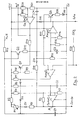
- Fig. 2 shows in more detail the clock and Evaluation module TAM, the structure and function of which will be described in more detail below.
- the working clock generator comprises an operational amplifier OpAm1 whose positive input is connected to a resistor connected between the operating voltage of the voltage divider R4, R5 and A whose output is fed back via a further resistor R3 to the positive input.
- the negative input of the operational amplifier OpAm1 is connected to the tap of an RC element connected between the operating voltage, which comprises a resistor R6 and a capacitor C2.
- the operational amplifier OpAm1 switches its output A to ground potential, so that the capacitor C2 discharges into the transmitter via a diode D2, a further diode D1 and a resistor R1.
- the dimensions of the components are such that, for example, a clock pulse of 50 ⁇ s is generated every 9 ms.
- the operating cycle can be changed by switching a comparator Komp1 with a signal on a line SN1 / 2 via a resistor R22, whereby an additional charging path, consisting of a resistor R7 and a diode D3, is activated to the capacitor C2. This shortens the cycle period to 3ms, for example.
- the time window is formed by a correspondingly connected comparator Komp2, the output of which is connected to the transmission line between the receiver and the switching amplifier and which, when actuated, keeps this line at ground potential.
- the positive input of the comparator Komp2 is connected to a voltage divider connected between the operating voltage, which comprises the resistors R16 and R17.
- the negative input of the comparator Komp2 is connected to a capacitor C3, to which a resistor R15 for discharge is connected in parallel. This parallel connection of capacitor C3 and resistor R15 is connected to the collector of a transistor Q1, the emitter of which is connected to the positive operating voltage (+ 12V).
- the base of transistor Q1 is connected to a voltage divider consisting of resistors R8 and R9, which are connected between the positive operating voltage and the output of operational amplifier OpAm1. If the output A of this operational amplifier OpAm1 is connected to ground when it is switched, the transistor Q1 opens and suddenly charges the capacitor C3 with the positive operating voltage. As a result, the comparator Komp2 switches, causing its output to reach ground potential and the time window to be closed.
- the operational amplifier OpAm1 switches again at its output A, and the transistor Q1 is closed. Now capacitor C3 discharges through resistor R15. This causes the comparator Komp2 to switch over and the time window is opened.
- a further transistor Q2 is operated, which is operated as a voltage follower and a charging of the capacitor C3 via a resistor R12 arranged in its emitter circuit causes.
- the capacitor C1 is charged via a resistor R2 and an adjustable potentiometer P1 from the positive operating voltage.
- the charging of the capacitor C1 can also be influenced from the outside via a line HuR and a resistor R13. For example, by applying a corresponding potential to this line, the transmission can be stopped completely or the closing time of the window can be changed. In normal operation, however, the charging of the capacitor C3 via the transistor Q2 and the resistor R12 at some point reaches a value at which the comparator Komp2 switches and sets its output to ground potential, which in turn closes the time window.
- the charging of the capacitor C3 is changed by the output of the output switching amplifier via a resistor R14 in order to generate a switching hysteresis, ie the closing time of the Time window is shifted.
- a filter with digital properties is specified by a capacitor C4, which is charged in stages by echo pulses received within the time window and, on the other hand, is discharged after each operating cycle via a diode D4 and a resistor R10 after the output A of the operational amplifier OpAm1.
- the dimensioning is such that the charge is sufficient to actuate a switching amplifier connected only after several received echo pulses.
- a diode D5 prevents discharge to the output of the comparator Komp2.
- a light-emitting diode LED indicates the reception of echo pulses by driving them with a non-switched comparator Komp2 a transistor Q3 at the base, which is connected in series with its collector / emitter path to a resistor R19 and the light-emitting diode LED, whereby the entire series connection is operated between the operating voltage.
- a Schmitt trigger is formed by an operational amplifier OpAm2, the negative input of which is connected to the capacitor C4 and the positive input of which is connected to a voltage divider consisting of the resistors R20 and R21, which are connected between the operating voltage.
- the exit of the Operational amplifier OpAm2 is fed back to the positive input via a resistor R18.
- the Schmitt trigger formed in this way generates a signal at its output when the charge on the capacitor C4 reaches a certain predeterminable value. This normally requires several echo pulses received within a time window.
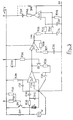
- the transmitting and receiving module SEM according to FIG. 3 has an essentially conventional structure and is only to be described in more detail insofar as it contains special features.
- Each operating cycle switches the full operating voltage to a coil L via a transistor Q4, so that the resulting voltage pulse excites the converter W to vibrate.
- a diode D11 is provided as a freewheeling diode.
- US echo pulses excite the transducer to vibrate and the electrical signals thus generated are fed to a first amplifier IC1 via a resistor R32 and a coupling capacitor C21.
- a tens diode D12 connected to ground serves to limit the input voltage of the amplifier IC1.
- a special feature is the switchable amplification factor of this amplifier. If a signal is applied via the second control line SN1 / 2, not only the operating clock frequency is increased, but also The transistor Q5 is controlled via the resistor R36, as a result of which the response sensitivity of the receiver is reduced in accordance with the shortening of the switching distance.
- a downstream amplifier IC2 is used for further amplification.
- a downstream dynamic comparator comprises an amplifier IC3, the positive input of which is connected to an RC element which consists of a high-resistance resistor R40 and a capacitor C27.
- the negative input of the amplifier IC3 is connected to a voltage divider, which consists of a low-resistance resistor R41 and a high-resistance resistor R42.
- Both the RC element (R40, C27) and the voltage divider (R41, R42) are connected in parallel to the capacitor C26.
- the voltage divider R41, R42 specifies the offset voltage.
- the whole arrangement acts as a filter, which only filters out the echoes and delivers them as positive standardized pulses to the clock and evaluation module. DC components in the received signal are not evaluated and high-frequency noise components are suppressed.
- the charging time of the capacitor C1 and thus also the charging time of the capacitor C3 can be controlled via the potentiometer P1, which leads to a shift in the closing time of the time window into the time t3 '. This is shown in broken lines in FIGS. 4b and 4c.
- the hysteresis specified via the output switching amplifier OpAm2 and the resistor R14 leads to a shift in the closing time t3 of the time window, which is not taken into account in FIG. 4c.
- RC elements were used to specify the work cycle and the time window.
- other timers such as counters, could be used to to specify the various switching points without using a digital counting method. It is important for the present US proximity switch to register one or more pulses within a predeterminable window, the transit time not being recorded digitally or in an analog manner. It is only determined whether the pulse is within the window; the window being adjustable and being broadened to obtain hysteresis when one or more pulses are received.
Landscapes
- Physics & Mathematics (AREA)
- Engineering & Computer Science (AREA)
- Radar, Positioning & Navigation (AREA)
- Remote Sensing (AREA)
- Acoustics & Sound (AREA)
- Computer Networks & Wireless Communication (AREA)
- General Physics & Mathematics (AREA)
- Electronic Switches (AREA)
- Measurement Of Velocity Or Position Using Acoustic Or Ultrasonic Waves (AREA)
Priority Applications (2)
| Application Number | Priority Date | Filing Date | Title |
|---|---|---|---|
| DE8888101969T DE3873739D1 (de) | 1988-02-11 | 1988-02-11 | Ultraschall-naeherungsschalter. |
| EP19880101969 EP0327656B1 (fr) | 1988-02-11 | 1988-02-11 | Commutateur de proximité à ultrasons |
Applications Claiming Priority (1)
| Application Number | Priority Date | Filing Date | Title |
|---|---|---|---|
| EP19880101969 EP0327656B1 (fr) | 1988-02-11 | 1988-02-11 | Commutateur de proximité à ultrasons |
Publications (2)
| Publication Number | Publication Date |
|---|---|
| EP0327656A1 true EP0327656A1 (fr) | 1989-08-16 |
| EP0327656B1 EP0327656B1 (fr) | 1992-08-12 |
Family
ID=8198713
Family Applications (1)
| Application Number | Title | Priority Date | Filing Date |
|---|---|---|---|
| EP19880101969 Expired - Lifetime EP0327656B1 (fr) | 1988-02-11 | 1988-02-11 | Commutateur de proximité à ultrasons |
Country Status (2)
| Country | Link |
|---|---|
| EP (1) | EP0327656B1 (fr) |
| DE (1) | DE3873739D1 (fr) |
Citations (7)
| Publication number | Priority date | Publication date | Assignee | Title |
|---|---|---|---|---|
| US3145363A (en) * | 1960-03-21 | 1964-08-18 | Kelvin & Hughes Ltd | Echo-sounding equipment |
| GB1139272A (en) * | 1966-05-20 | 1969-01-08 | Lab For Electronics Inc | Sonic vehicle detector |
| US3555499A (en) * | 1968-05-24 | 1971-01-12 | Texas Instruments Inc | Method and system for determining reflectivity of the ocean bottom |
| US3793618A (en) * | 1972-10-30 | 1974-02-19 | Heath Co | Depth alarm system |
| DE2344702A1 (de) * | 1973-09-05 | 1975-03-06 | Dirk Bruehl | Verfahren und schaltungsanordnung zur erzielung einer anzeige von stark gestoerten periodisch wiederkehrenden signalen |
| US4326273A (en) * | 1980-07-23 | 1982-04-20 | Hurst Performance, Inc. | Ultrasonic ranging device |
| US4551722A (en) * | 1982-03-16 | 1985-11-05 | Nippondenso Co., Ltd. | Apparatus and method for detecting obstacles in the path of a moving vehicle |
-
1988
- 1988-02-11 DE DE8888101969T patent/DE3873739D1/de not_active Expired - Fee Related
- 1988-02-11 EP EP19880101969 patent/EP0327656B1/fr not_active Expired - Lifetime
Patent Citations (7)
| Publication number | Priority date | Publication date | Assignee | Title |
|---|---|---|---|---|
| US3145363A (en) * | 1960-03-21 | 1964-08-18 | Kelvin & Hughes Ltd | Echo-sounding equipment |
| GB1139272A (en) * | 1966-05-20 | 1969-01-08 | Lab For Electronics Inc | Sonic vehicle detector |
| US3555499A (en) * | 1968-05-24 | 1971-01-12 | Texas Instruments Inc | Method and system for determining reflectivity of the ocean bottom |
| US3793618A (en) * | 1972-10-30 | 1974-02-19 | Heath Co | Depth alarm system |
| DE2344702A1 (de) * | 1973-09-05 | 1975-03-06 | Dirk Bruehl | Verfahren und schaltungsanordnung zur erzielung einer anzeige von stark gestoerten periodisch wiederkehrenden signalen |
| US4326273A (en) * | 1980-07-23 | 1982-04-20 | Hurst Performance, Inc. | Ultrasonic ranging device |
| US4551722A (en) * | 1982-03-16 | 1985-11-05 | Nippondenso Co., Ltd. | Apparatus and method for detecting obstacles in the path of a moving vehicle |
Also Published As
| Publication number | Publication date |
|---|---|
| EP0327656B1 (fr) | 1992-08-12 |
| DE3873739D1 (de) | 1992-09-17 |
Similar Documents
| Publication | Publication Date | Title |
|---|---|---|
| EP0033508B1 (fr) | Circuit pour transmettre et recevoir alternativement avec un seul émetteur-transducteur du son | |
| DE19520940C2 (de) | Anordnung zur galvanisch getrennten Übertragung von Hilfsenergie (Gleichspannung) und Informationen zu einer elektronischen Einheit | |
| EP0168895B1 (fr) | Dispositif d'aide auditive | |
| DE2634240C2 (de) | Signalauswahl- und Fernmelde-Dekodiersystem zur Auswahl von wenigstens einem aus mehreren zu überwachenden Signalen | |
| DE2721225A1 (de) | Schaltungsanordnung zur frequenz- selbststeuerung eines ultraschall- sendewandlers | |
| DE2251094C2 (de) | Fernsteuer-Empfangsschaltung zur Unterscheidung zwischen Störsignalen und Nutzsignalen | |
| DE3909807A1 (de) | Fernsteuerung | |
| EP1238468B1 (fr) | Procede et systeme pour l'antiparasitage dans un circuit recepteur | |
| DE3513270A1 (de) | Einrichtung zur abstandsmessung, insbesondere fuer kraftfahrzeuge | |
| DE2801122A1 (de) | Fernwirksystem zum selektiven ansteuern von verbrauchern, insbesondere in einem kraftfahrzeug | |
| DE2813628A1 (de) | Filterschaltung | |
| DE2433362A1 (de) | Schaltungsanordnung zum erzeugen eines ausgangssignales aus einem eingangssignal mit vorgegebener frequenz und unterschiedlich grossen amplituden | |
| CH632626A5 (de) | Fernsteuerungssender. | |
| EP0469174A1 (fr) | Procédé pour commander à distance une prothèse auditive | |
| DE2752522C2 (de) | Abstimmbarer Tonsignaldetektor | |
| EP0623395B1 (fr) | Circuit pour amortir un transducteur d'ultrasons | |
| DE2622868A1 (de) | Digitale steuereinrichtung | |
| CH635454A5 (de) | Fernsteuerungsempfaenger. | |
| DE1948180A1 (de) | Einzelfrequenz-Zeichengabeempfaenger | |
| EP0327656B1 (fr) | Commutateur de proximité à ultrasons | |
| DE3234152C2 (fr) | ||
| DE69028393T2 (de) | Verfahren und gerät zur diskriminierung eines datensignals | |
| DE3608440C2 (fr) | ||
| DE2912566A1 (de) | Ton-decodierschaltung | |
| DE1904836C3 (de) | Laufzeit-MeBvorrfchtung zur Ultraschallprüfung von Beton |
Legal Events
| Date | Code | Title | Description |
|---|---|---|---|
| PUAI | Public reference made under article 153(3) epc to a published international application that has entered the european phase |
Free format text: ORIGINAL CODE: 0009012 |
|
| AK | Designated contracting states |
Kind code of ref document: A1 Designated state(s): AT BE CH DE ES FR GB GR IT LI LU NL SE |
|
| 17P | Request for examination filed |
Effective date: 19890725 |
|
| RBV | Designated contracting states (corrected) |
Designated state(s): CH DE FR GB LI |
|
| 17Q | First examination report despatched |
Effective date: 19910809 |
|
| GRAA | (expected) grant |
Free format text: ORIGINAL CODE: 0009210 |
|
| AK | Designated contracting states |
Kind code of ref document: B1 Designated state(s): CH DE FR GB LI |
|
| GBT | Gb: translation of ep patent filed (gb section 77(6)(a)/1977) | ||
| REF | Corresponds to: |
Ref document number: 3873739 Country of ref document: DE Date of ref document: 19920917 |
|
| ET | Fr: translation filed | ||
| PGFP | Annual fee paid to national office [announced via postgrant information from national office to epo] |
Ref country code: FR Payment date: 19921215 Year of fee payment: 6 |
|
| PGFP | Annual fee paid to national office [announced via postgrant information from national office to epo] |
Ref country code: GB Payment date: 19921221 Year of fee payment: 6 Ref country code: CH Payment date: 19921221 Year of fee payment: 6 |
|
| PLBE | No opposition filed within time limit |
Free format text: ORIGINAL CODE: 0009261 |
|
| STAA | Information on the status of an ep patent application or granted ep patent |
Free format text: STATUS: NO OPPOSITION FILED WITHIN TIME LIMIT |
|
| 26N | No opposition filed | ||
| PG25 | Lapsed in a contracting state [announced via postgrant information from national office to epo] |
Ref country code: GB Effective date: 19940211 |
|
| PG25 | Lapsed in a contracting state [announced via postgrant information from national office to epo] |
Ref country code: LI Effective date: 19940228 Ref country code: CH Effective date: 19940228 |
|
| GBPC | Gb: european patent ceased through non-payment of renewal fee |
Effective date: 19940211 |
|
| PG25 | Lapsed in a contracting state [announced via postgrant information from national office to epo] |
Ref country code: FR Effective date: 19941031 |
|
| REG | Reference to a national code |
Ref country code: CH Ref legal event code: PL |
|
| REG | Reference to a national code |
Ref country code: FR Ref legal event code: ST |
|
| PGFP | Annual fee paid to national office [announced via postgrant information from national office to epo] |
Ref country code: DE Payment date: 19960130 Year of fee payment: 9 |
|
| PG25 | Lapsed in a contracting state [announced via postgrant information from national office to epo] |
Ref country code: DE Effective date: 19971101 |