EP0327675A2 - Membrane de blindage - Google Patents
Membrane de blindage Download PDFInfo
- Publication number
- EP0327675A2 EP0327675A2 EP88116318A EP88116318A EP0327675A2 EP 0327675 A2 EP0327675 A2 EP 0327675A2 EP 88116318 A EP88116318 A EP 88116318A EP 88116318 A EP88116318 A EP 88116318A EP 0327675 A2 EP0327675 A2 EP 0327675A2
- Authority
- EP
- European Patent Office
- Prior art keywords
- radiation
- layer
- absorption
- shielding membrane
- deflection
- Prior art date
- Legal status (The legal status is an assumption and is not a legal conclusion. Google has not performed a legal analysis and makes no representation as to the accuracy of the status listed.)
- Withdrawn
Links
Images

Classifications
-
- H—ELECTRICITY
- H05—ELECTRIC TECHNIQUES NOT OTHERWISE PROVIDED FOR
- H05K—PRINTED CIRCUITS; CASINGS OR CONSTRUCTIONAL DETAILS OF ELECTRIC APPARATUS; MANUFACTURE OF ASSEMBLAGES OF ELECTRICAL COMPONENTS
- H05K9/00—Screening of apparatus or components against electric or magnetic fields
- H05K9/0073—Shielding materials
- H05K9/0081—Electromagnetic shielding materials, e.g. EMI, RFI shielding
- H05K9/0088—Electromagnetic shielding materials, e.g. EMI, RFI shielding comprising a plurality of shielding layers; combining different shielding material structure
Definitions
- the present invention relates generally to a device for shielding electromagnetic radiation emanating from electronic devices and electrical power sources. More particularly, the present invention relates to a shielding membrane that absorbs undesirable radiation emitted by cathode ray tubes, power sources and other electronic equipment systems.
- an electromagnetic wave absorber comprised of a plurality of foamed polystyrol members sandwiched between a metallic plate and a front surface having a plurality of pyramidal shaped foam surfaces created from the same material as the wave absorbing members.
- the polystyrol members serve as radiation absorbing media.
- the metallic layer reflects radiation incident thereon.
- Japanese Patent Application No. 55-29599 discloses an alternative embodiment of a wave absorber that comprises a plurality of triangular pyramid shape ferrite members disposed over ferrite plates that are backed with a metal plate. While such a device would effectively absorb some frequencies, its reliance upon wave length matching principles (due to its ferrite composition), restricts its usefulness to limited frequency ranges.
- Another object of the invention is to provide a housing suitable for shielding users from radiation emitted by electronic appliances.
- Another object of the present invention is to provide a shielding membrane that minimizes reflections back to a radiation source.
- Another object of the invention is to provide a shielding membrane with a low radiation transmissivity.
- a shielding membrane for shielding radiation from an electromagnetic radiation source.
- the shielding membrane has an incident surface facing the radiation source and a base surface facing away from the radiation source.
- the shielding membrane includes means for minimizing reflection of radiation directed onto the incident surface of the shielding membrane.
- Means is also provided for grounding some of the low frequency electrical components of the radiation.
- a conductive deflection layer formed of a multiplicity of spaced-apart metallic deflection pads adapted to deflect incident radiation thereabout, is stacked behind the low frequency grounding means.
- a conductive absorption funneling layer is positioned spaced apart behind the deflection layer in a confronting relationship.
- the absorption funneling layer includes a multiplicity of apertures for passing radiation deflected about the deflection pads.
- a reflecting plate is placed near the base side of the absorption funneling layer.
- the low frequency grounding means, the deflection layer, the absorption funneling layer and the reflecting plate are each spaced apart and grounded to facilitate absorption of various components of the incident radiation.
- the gaps between these conductive layers are filled by spacers that are formed of an absorbing media to maximize radiation absorption.
- the spacers are formed of a high density porous foam.
- the low frequency grounding means preferably includes a conductive mesh.
- the reflection minimizing means preferably includes a waveguide barrier having a multiplicity of protrusions facing the radiation emitting source.
- the protrusions are preferably pyramidal in shape and the waveguide barrier is preferably formed of a high density porous foam.
- the apertures in the absorption funneling layer preferably have the same geometry as the deflection pads on the deflection layer.
- the apertures in the absorption funneling layer are stamped from a metallic foil and the cutout foil materials are used to form the deflection pads in the deflection layer.
- Such a shielding membrane may be used to shield video display terminals, power supply stations, electronic equipment and the like. Additionally the walls of buildings and/or rooms, ships, aircraft, and other vehicles that require data and detection security could be constructed to incorporate such a shielding device.
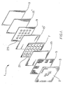
- the shielding membrane 1 of the present invention includes a waveguide barrier 3, a mesh 5, a deflection layer 7, an absorption funneling layer 9, a reflecting plate 11, and a plurality of absorption spacers 15, 15′, 15 ⁇ formed from an appropriate absorption media.
- the mesh, the deflective layer, the absorption funneling layer and the reflecting plate (referred to herein as the conductive layers) are all formed of highly conductive materials and grounded and spacers 15, 15′ and 15 ⁇ are disposed therebetween to absorb and disperse as much of the incident radiation as possible.
- the shielding membrane described is designed to suppress radiation over an extremely broad frequency range including high frequency radiation near the visible light spectrum and extremely low frequency waves.
- the shielding membrane 1 has an incident surface 2 facing toward the components that emit radiation sought to be suppressed and an base surface.
- Waveguide barrier 3 forms the incident surface 2 of the shielding membrane 1.
- the waveguide includes a plurality of pyramid shaped protrusions that face toward the radiation emitting source (not shown). The shape of the protrusions may be varied somewhat, although they are intended to minimize radiation reflections from the incident surface of the shielding membrane 1 as described below with relation to Figure 4.
- the waveguide barrier is formed from a radiation absorbing material preferably having micropores dispersed therethrough. The micropores are used advantageously to disperse radiation within the shielding membrane 1 which enhances the likelihood of absorption.
- a mesh 5 formed of a highly electrically conductive material such as a conductive plastic or metal is disposed behind the waveguide barrier 3.
- suitable metals include copper, aluminum, steel, conductively coated nylon or polyester, etc.
- Suitable plastics include foam and composites.
- the mesh is grounded and as will be appreciated by those familiar with antenna theory, the mesh will appear as a grounding plate to low frequency radiation. Therefore, a substantial percentage of the low frequency radiation incident upon conductive mesh 5 will be absorbed thereby.
- waveguide barrier 3 may be provided with and adhesive backing which adheres to the mesh 5.
- a suitable adhesive is a 9000 Series type adhesive manufactured by 3M Company of St. Paul, Minnesota.
- a deflection layer 7 formed of a plurality of electrically conductive deflection pads 21 is disposed on the base side of spacer 15.
- a spacer 15 formed of a radiation absorbing medium is disposed between the mesh 5 and the deflection layer 7 to separate the deflection layer and maintain a suitable distance therebetween. It should be appreciated that the actual spacing may be widely varied. By way of example, a 1/8" separation is appropriate.
- the deflection pads 21 are in electrical contact with one another and are suitably grounded. The electrical contact may be maintained by any suitable means including a conductive copper tape or a wire mesh.
- the deflection layer 7 is preferably formed of a metallic material such as copper, aluminum, stainless steel or nickel, (although other conductors are appropriate).
- the actual size of the deflection pads may be widely varied although, as explained below, they should be sized such that the expected incident radiation will deflect thereabout.
- the deflection pads may take any geometric shape. By way of example, a circular shape has been found to work well. Further by way of example, 2 cm. diameter disks work well for most applications.
- the deflection pads 21 must be spaced apart to work effectively. Experimentation has shown that a spacing of approximately one-fourth the disk diameter works well. Thus, for the 2 cm. diameter disks described above, a 0.5 cm. spacing works well. However, it should be appreciated that the actual size, shape and spacing of the deflection pads 21 may be widely varied.
- the actual size of the pads chosen for a particular function may be, in part, dependent on the wavelength of radiations sought to be suppressed.
- Absorption funneling layer 9 includes a plurality of apertures 25 and is spaced apart from the deflection layer 7 on its base side.
- a second spacer 15′ is disposed between the deflection layer 7 and the absorption funneling layer 9 to maintain the desired spacing.
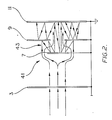
- the spacing between absorption funneling layer 9 and deflection layer 7 is chosen to allow radiation deflected about the deflection pads 21 to recombine such that a substantial percentage of such radiation will regroup and pass through apertures 25.
- a suitable separation is at least 1/8".
- a reflecting plate 11 is positioned on the base side of the absorption funneling layer 9 with an appropriate spacer 15 ⁇ disposed therebetween.
- the purpose of the reflective layer 11 is to reflect any incident radiation that is not absorbed thereon.
- the deflection layer 7, absorption funneling layer 9 and reflective plate 11 cooperate to trap entering radiation between the deflection layer and the reflective plate. A substantial portion of the trapped radiation is reflected back and forth between deflection layer 7 and the reflective plate until it is ultimately absorbed.
- Mesh 5, deflection layer 7, absorption funneling layer 9 and reflective plate 11 are all connected to appropriate grounds which may take the form of a common ground.
- the spacers 15, 15′ and 15 ⁇ are all formed of a radiation absorbing media.
- desirable spacer properties include the ability to effectively absorb and disperse radiation incident thereon.
- suitable radiation absorbing materials are known to the art and, by way of example, a high density porous foam felt, fiberglass and the like all work well.
- the spacers may be formed of either conductive or nonconductive material.
- Soundfoam manufactured by Soundfoam of Los Angeles, California works well.
- the deflection pads, the absorption funneling layer and the reflective plate 11 are all preferably stippled to enhance defraction of radiation within the shielding membrane.
- the shielding membrane 1 is broken down into several distinct regions.
- the first region (which comprises waveguide barrier 3) insures that, radiation incident on the shielding membrane is not reflected back towards the source of EM radiation. It is important to minimize the reflection of radiation back towards the source since such radiations may appear as noise to the source.
- the waveguide barrier 3, as well as the spacers 15, are formed from a media that absorbs and disperses radiation passing therethrough. Dispersion of the radiation is important since it statistically increases the likelihood that incident radiation will be either absorbed or grounded within the shielding membrane. Therefore, the waveguide barrier acts as both an initial reflection minimizing zone and as an absorption and dispersion zone.
- the mesh 5 acts as a grounding zone for low frequency radiation.
- a wire mesh will effectively ground much of the incident low frequency radiation.
- Higher frequency radiation (and lower frequency radiation that escapes the mesh) passes through an absorption spacer into a trap region comprising the deflection layer 7, absorption funneling layer 9, and reflecting plate 11.
- the intent of the trap region is to "capture" a substantial portion of the incident radiation behind the deflection and preferably the absorption funneling layer to ensure that it is absorbed rather than reflected back towards the radiation source or transmitted outside the shield.
- the deflection pads 21 create a deflection zone 41. Radiation that passes through the deflection zone 41 travels into a funneling zone 43 which directs the radiation through apertures 25 in absorption funneling layer 9. The radiation tend to regroup after it passes the deflection pads and pass through the apertures 25 in absorption funneling layer 9. Such regrouping is important to the function of the trap, since the intent is to have radiation deflected about the deflection pads 21 pass through the apertures 25. Therefore, it is important that the absorption funneling layer be spaced far enough behind the deflection pads to allow the radiation to regroup and divert through the apertures 25.
- the waves After passing through the funneling zone the waves pass into a second absorption zone disposed between the absorption funneling layer and the reflecting plate 11.
- the intent is to trap as much of the radiation as possible between the reflective plate 11 and the deflection layer 7 and to cause the radiation trapped therein to bounce back and forth between the reflecting plate and the absorption funneling layer until it is absorbed.
- the described construction proves to be very effective at retaining radiation within the second absorption zone long enough for it to be either absorbed by spacer 15 or grounded by one of the conductive layers.
- the waveguide includes a plurality of pyramid shaped protrusions 32 that face toward the radiation emitting source (not shown).
- the shape of the protrusions may be varied somewhat, although they are intended to minimize radiation reflections from the incident surface of the shielding membrane 1.
- the waveguide barrier 3 is formed from a radiation absorbing material preferably having micropores dispersed therethrough. The micropores are used advantageously to disperse radiation within the shielding membrane 1 which enhances the likelihood of absorption.
- suitable radiation absorbing materials are known to the art and by way of example, a high density porous foam works well for this purpose.
- a suitable high density foam is Soundfoam, manufactured by Soundfoam of Los Angeles, California.
- Other suitable materials include felt, fiberglass and the like.
- the waveguide barrier includes a multiplicity of pyramidal shaped protrusions that face the radiation emitting source. Such a shape reduces the likelihood of reflecting radiation back toward the radiation source.
- the pyramidal geometry facilitates increased absorption since radiation reflected off of the incident surface 2 is likely to be reflected toward another portion of the waveguide barrier 3 wherein it may be absorbed on its second or third contact.
- the advantages of such a construction is well known to the prior art. It is important to minimize reflections since such radiation constitutes noise which in many circumstances can be extremely problematic for the electronics.
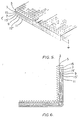
- Membrane sections may be interlinked by using continuous conducting layers including conductive mesh 5, deflection layer 7, absorption funneling layer 9 and reflective layer 11.
- the waveguide barrier and the spacers may be sized appropriately to conform to the walls of a housing.
- two adjoining sections are bent upon another as shown in Figure 6 such that the respective waveguide barriers 3 contact one another.
- Such a continuous construction minimizes the possibility of both reflection back toward the electrical components and emissions of radiation from the appliance.
- each of the conducting layers may be joined to a common ground.
- the spacers do not have to be cut for corner bending as long as they stretch sufficiently to accommodate the extra distance required.
- the sandwich construction described may be manufactured in a laminated form, as individual components or in other suitable forms.
- a metallic foil sheet may be used to form absorption funneling layer 9, with the apertures 25 being punched therefrom.
- the punched portions of the metallic foil may be used to form the deflection pads 21.
- the stamped portions of the absorption funneling layer are moved forward and electrically connected by suitable means such as copper or other conductive tape or wire.
- the shielding membrane may be fabricated in a tubular construction. Such a tubular configuration lends itself ideally to the shielding of power lines, conduits and the like.
- the application of a shielding membrane to the plastic casing walls of a video display terminal will be described.
- a thin layer of adhesive is applied to the back surface of the reflecting plate as uniformly as possible.
- the shielding layer is then adhered to the casing wall.
- the shielding membrane 1 may be integrated into the housing of an electrical appliance.
- the present invention may be embodied in many other specific forms without departing from the spirit or scope of the invention. Particularly, it should be appreciated that additional absorption or grounding layers could be added to further reduce reflections or transmissivity. Similarly, multiple defraction/absorption funneling component pairs may be added to improve the efficiency of the shielding membrane. It should also be appreciated that there are a wide variety of materials that can be used for each of the components. For example, the waveguide barrier and spacers may be formed from high density foams, felt, fiberglass or even particle board. The various conducting layers should all be highly conductive, such as metal mesh and foils.
- the conductive layers 5, 7 9 and 11 may be formed of lead. Such a construction would greatly reduce the weight of conventional shielding aprons necessary to protect against X-rays. It will be appreciated that the multi-layer structure of spaced conductive layers obviates the need for an individual conductive barrier layer that is very thick as is commonly necessary in conventional single layer X-ray barriers.
- a shielding membrane as disclosed herein has many applications beyond housings for cathode ray tubes and electronic components as described herein.
- a shield arrangement could be built into the walls of power stations to reduce the fields generated therein.
- installations which have concerns about the security of data may include walls formed with the described shielding membrane to prevent the escape of radiation.
- vehicles and installations can be shielded from electronic jamming with such a membrane.
- the shielding membrane of the present invention may be used to attenuate certain electromagnetic fields. This is accomplished by suppressing the electrical components of such fields.
Landscapes
- Physics & Mathematics (AREA)
- Electromagnetism (AREA)
- Engineering & Computer Science (AREA)
- Microelectronics & Electronic Packaging (AREA)
- Shielding Devices Or Components To Electric Or Magnetic Fields (AREA)
- Thin Magnetic Films (AREA)
Applications Claiming Priority (2)
| Application Number | Priority Date | Filing Date | Title |
|---|---|---|---|
| US07/154,977 US4825090A (en) | 1988-02-09 | 1988-02-09 | Shielding membrane |
| US154977 | 1988-02-09 |
Publications (2)
| Publication Number | Publication Date |
|---|---|
| EP0327675A2 true EP0327675A2 (fr) | 1989-08-16 |
| EP0327675A3 EP0327675A3 (fr) | 1990-01-31 |
Family
ID=22553623
Family Applications (1)
| Application Number | Title | Priority Date | Filing Date |
|---|---|---|---|
| EP88116318A Withdrawn EP0327675A3 (fr) | 1988-02-09 | 1988-10-04 | Membrane de blindage |
Country Status (4)
| Country | Link |
|---|---|
| US (1) | US4825090A (fr) |
| EP (1) | EP0327675A3 (fr) |
| JP (1) | JPH025597A (fr) |
| AU (1) | AU599529B2 (fr) |
Cited By (3)
| Publication number | Priority date | Publication date | Assignee | Title |
|---|---|---|---|---|
| EP0536541B1 (fr) * | 1991-10-05 | 1997-01-08 | BESMA BESCHICHTUNGSMASSEN GmbH | Feuille déformable pour accrocher sur un support et protéger contre les rayonnements ou isoler des parties électriquement conductrices |
| RU2168879C1 (ru) * | 2000-09-20 | 2001-06-10 | Спирин Юрий Леонидович | Устройство для защиты от электромагнитного излучения |
| ITBO20110665A1 (it) * | 2011-11-21 | 2013-05-22 | Nrg En S R L | Dispositivo di schermatura per campi elettromagnetici ed elettrostatici |
Families Citing this family (17)
| Publication number | Priority date | Publication date | Assignee | Title |
|---|---|---|---|---|
| JPH0634152Y2 (ja) * | 1988-12-08 | 1994-09-07 | 多機能カード | |
| US5098735A (en) * | 1990-09-14 | 1992-03-24 | Advanced Research Technologies | Shielding of houses and buildings from low and high frequency EMF radiation by organic based stabilized nickel conductive coatings |
| US5274420A (en) * | 1992-04-20 | 1993-12-28 | International Business Machines Corporation | Beamsplitter type lens elements with pupil-plane stops for lithographic systems |
| CA2154156C (fr) * | 1993-02-02 | 2005-04-26 | Edward D. Suski | Carte de circuit a grilles de blindage et sa methode de fabrication |
| US5334800A (en) * | 1993-07-21 | 1994-08-02 | Parlex Corporation | Flexible shielded circuit board |
| US5519168A (en) * | 1993-10-12 | 1996-05-21 | Owens; William M. | Electromagnetic interference shielding |
| US5583318A (en) * | 1993-12-30 | 1996-12-10 | Lucent Technologies Inc. | Multi-layer shield for absorption of electromagnetic energy |
| US5539150A (en) * | 1995-01-18 | 1996-07-23 | American Etching & Manufacturing | Kit and method of making radiation shields |
| US5473110A (en) * | 1995-03-07 | 1995-12-05 | Unisys Corporation | Magnetically-attachable EMI shielding cover for attenuating electromagnetic emanation |
| US5675299A (en) * | 1996-03-25 | 1997-10-07 | Ast Research, Inc. | Bidirectional non-solid impedance controlled reference plane requiring no conductor to grid alignment |
| SE520785C2 (sv) * | 2000-05-22 | 2003-08-26 | Ericsson Telefon Ab L M | Täcklock för en elektronikanordning |
| US6671186B2 (en) * | 2001-04-20 | 2003-12-30 | Hewlett-Packard Development Company, L.P. | Electromagnetic interference shield |
| JP4738636B2 (ja) * | 2001-05-29 | 2011-08-03 | 株式会社テクノ菱和 | 防爆型無発塵イオナイザー |
| JP4098788B2 (ja) * | 2005-05-09 | 2008-06-11 | Tdk株式会社 | 電波減衰体 |
| TWI631889B (zh) * | 2014-12-27 | 2018-08-01 | 中原大學 | Electromagnetic wave shielding composite film |
| US20180338396A1 (en) * | 2017-05-16 | 2018-11-22 | Murata Manufacturing Co., Ltd. | Electronic component having electromagnetic shielding and method for producing the same |
| JP2025069659A (ja) * | 2023-10-18 | 2025-05-01 | コグニティブリサーチラボ株式会社 | 電磁波遮断構造体 |
Family Cites Families (7)
| Publication number | Priority date | Publication date | Assignee | Title |
|---|---|---|---|---|
| JPS523706Y2 (fr) * | 1973-09-14 | 1977-01-26 | ||
| US3964072A (en) * | 1975-02-25 | 1976-06-15 | General Electric Company | Suppression of unwanted radiation from unavoidable openings in shielded enclosures |
| DE2946519C2 (de) * | 1979-11-17 | 1983-05-11 | Leo 5000 Köln Wirtz | Fenster mit elektromagnetischer und akustischer Abschirmung |
| DE3133441C2 (de) * | 1981-08-24 | 1984-02-02 | Precitronic Gesellschaft für Feinmechanik und Electronic mbH, 2000 Hamburg | Abschirmung gegen elektromagnetische Impulse |
| US4647714A (en) * | 1984-12-28 | 1987-03-03 | Sohwa Laminate Printing Co., Ltd. | Composite sheet material for magnetic and electronic shielding and product obtained therefrom |
| US4631641A (en) * | 1985-07-18 | 1986-12-23 | Northern Telecom Limited | Electronic apparatus with electro-magnetic interference screening |
| JPH101706A (ja) * | 1996-06-12 | 1998-01-06 | Kawasaki Steel Corp | 溶銑予備処理時の排ガス集塵装置 |
-
1988
- 1988-02-09 US US07/154,977 patent/US4825090A/en not_active Expired - Fee Related
- 1988-10-04 EP EP88116318A patent/EP0327675A3/fr not_active Withdrawn
-
1989
- 1989-02-08 AU AU29760/89A patent/AU599529B2/en not_active Ceased
- 1989-02-09 JP JP1030910A patent/JPH025597A/ja active Pending
Cited By (3)
| Publication number | Priority date | Publication date | Assignee | Title |
|---|---|---|---|---|
| EP0536541B1 (fr) * | 1991-10-05 | 1997-01-08 | BESMA BESCHICHTUNGSMASSEN GmbH | Feuille déformable pour accrocher sur un support et protéger contre les rayonnements ou isoler des parties électriquement conductrices |
| RU2168879C1 (ru) * | 2000-09-20 | 2001-06-10 | Спирин Юрий Леонидович | Устройство для защиты от электромагнитного излучения |
| ITBO20110665A1 (it) * | 2011-11-21 | 2013-05-22 | Nrg En S R L | Dispositivo di schermatura per campi elettromagnetici ed elettrostatici |
Also Published As
| Publication number | Publication date |
|---|---|
| US4825090A (en) | 1989-04-25 |
| AU2976089A (en) | 1989-08-10 |
| JPH025597A (ja) | 1990-01-10 |
| EP0327675A3 (fr) | 1990-01-31 |
| AU599529B2 (en) | 1990-07-19 |
Similar Documents
| Publication | Publication Date | Title |
|---|---|---|
| US4825090A (en) | Shielding membrane | |
| US5563614A (en) | Low noise dual polarization electromagnetic power reception and conversion system | |
| US5522602A (en) | EMI-shielding gasket | |
| US4381421A (en) | Electromagnetic shield for electronic equipment | |
| US6504501B2 (en) | Radio wave absorbing panel | |
| US6297446B1 (en) | High performance EMC vent panel | |
| JPS61140203A (ja) | 抵抗性ループ角度フイルタ | |
| WO2019172237A1 (fr) | Couvercle de radar à ondes millimétriques | |
| US6825411B2 (en) | Method and apparatus for controlling electromagnetic radiation emissions from electronic device enclosures | |
| CN114447622A (zh) | 一种宽带超薄透明吸波体设计 | |
| KR20230031493A (ko) | 전자파 및 자기장 흡수차폐시트 및 이를 포함하는 전자기기 | |
| US10439292B2 (en) | Electromagnetic energy shielding systems, apparatuses, and methods | |
| CN112739183A (zh) | 电磁干扰薄板衰减器 | |
| EP1028611B1 (fr) | Plaque-écran électromagnétique transparente | |
| JP2972305B2 (ja) | 電磁遮へい体および電磁遮へい用筐体 | |
| JP2001053485A (ja) | 電磁波吸収シート | |
| JPH11261283A (ja) | 反射波干渉低減型電磁遮蔽建物 | |
| EP0425262B1 (fr) | Absorbeurs | |
| JP2003078276A (ja) | 電波吸収体 | |
| JPH10126091A (ja) | 電磁シールド性能を有する窓ガラス | |
| JP4487345B2 (ja) | 電波暗室 | |
| EP1195848B1 (fr) | Paroi équipée d' absorbeur de micro-ondes | |
| JPH025033B2 (fr) | ||
| RU2821816C1 (ru) | Экран | |
| JP4487346B2 (ja) | 電波無響箱 |
Legal Events
| Date | Code | Title | Description |
|---|---|---|---|
| PUAI | Public reference made under article 153(3) epc to a published international application that has entered the european phase |
Free format text: ORIGINAL CODE: 0009012 |
|
| AK | Designated contracting states |
Kind code of ref document: A2 Designated state(s): AT BE CH DE ES FR GB GR IT LI LU NL SE |
|
| PUAL | Search report despatched |
Free format text: ORIGINAL CODE: 0009013 |
|
| AK | Designated contracting states |
Kind code of ref document: A3 Designated state(s): AT BE CH DE ES FR GB GR IT LI LU NL SE |
|
| 17P | Request for examination filed |
Effective date: 19900306 |
|
| 17Q | First examination report despatched |
Effective date: 19910711 |
|
| RAP1 | Party data changed (applicant data changed or rights of an application transferred) |
Owner name: GRABIS, DIETRICH WALTER |
|
| RAP1 | Party data changed (applicant data changed or rights of an application transferred) |
Owner name: GRABIS, DIETRICH WALTER |
|
| STAA | Information on the status of an ep patent application or granted ep patent |
Free format text: STATUS: THE APPLICATION IS DEEMED TO BE WITHDRAWN |
|
| 18D | Application deemed to be withdrawn |
Effective date: 19940501 |