EP0328633B1 - Cellule matricielle active pour fonctionnement en courant alternatif - Google Patents
Cellule matricielle active pour fonctionnement en courant alternatif Download PDFInfo
- Publication number
- EP0328633B1 EP0328633B1 EP88908540A EP88908540A EP0328633B1 EP 0328633 B1 EP0328633 B1 EP 0328633B1 EP 88908540 A EP88908540 A EP 88908540A EP 88908540 A EP88908540 A EP 88908540A EP 0328633 B1 EP0328633 B1 EP 0328633B1
- Authority
- EP
- European Patent Office
- Prior art keywords
- liquid crystal
- crystal display
- common
- top plate
- signal
- Prior art date
- Legal status (The legal status is an assumption and is not a legal conclusion. Google has not performed a legal analysis and makes no representation as to the accuracy of the status listed.)
- Expired - Lifetime
Links
- 239000011159 matrix material Substances 0.000 title abstract description 9
- 239000004973 liquid crystal related substance Substances 0.000 claims abstract description 73
- 210000004027 cell Anatomy 0.000 claims abstract description 41
- 239000003990 capacitor Substances 0.000 claims abstract description 24
- 210000002858 crystal cell Anatomy 0.000 claims abstract description 19
- 238000000034 method Methods 0.000 claims description 5
- XUIMIQQOPSSXEZ-UHFFFAOYSA-N Silicon Chemical compound [Si] XUIMIQQOPSSXEZ-UHFFFAOYSA-N 0.000 claims 1
- 229910044991 metal oxide Inorganic materials 0.000 claims 1
- 150000004706 metal oxides Chemical group 0.000 claims 1
- 229910052710 silicon Inorganic materials 0.000 claims 1
- 239000010703 silicon Substances 0.000 claims 1
- 230000005669 field effect Effects 0.000 abstract description 6
- 238000010586 diagram Methods 0.000 description 7
- 239000000463 material Substances 0.000 description 7
- 230000000694 effects Effects 0.000 description 4
- 230000004913 activation Effects 0.000 description 3
- VYPSYNLAJGMNEJ-UHFFFAOYSA-N Silicium dioxide Chemical compound O=[Si]=O VYPSYNLAJGMNEJ-UHFFFAOYSA-N 0.000 description 2
- 230000010354 integration Effects 0.000 description 2
- 230000001360 synchronised effect Effects 0.000 description 2
- 230000006978 adaptation Effects 0.000 description 1
- 230000015556 catabolic process Effects 0.000 description 1
- 229910052681 coesite Inorganic materials 0.000 description 1
- 239000000356 contaminant Substances 0.000 description 1
- 229910052906 cristobalite Inorganic materials 0.000 description 1
- 238000006731 degradation reaction Methods 0.000 description 1
- 230000009977 dual effect Effects 0.000 description 1
- 238000010894 electron beam technology Methods 0.000 description 1
- 239000012212 insulator Substances 0.000 description 1
- 238000012986 modification Methods 0.000 description 1
- 230000004048 modification Effects 0.000 description 1
- 239000000377 silicon dioxide Substances 0.000 description 1
- 230000003068 static effect Effects 0.000 description 1
- 229910052682 stishovite Inorganic materials 0.000 description 1
- 239000000126 substance Substances 0.000 description 1
- 229910052905 tridymite Inorganic materials 0.000 description 1
Images


Classifications
-
- G—PHYSICS
- G09—EDUCATION; CRYPTOGRAPHY; DISPLAY; ADVERTISING; SEALS
- G09G—ARRANGEMENTS OR CIRCUITS FOR CONTROL OF INDICATING DEVICES USING STATIC MEANS TO PRESENT VARIABLE INFORMATION
- G09G3/00—Control arrangements or circuits, of interest only in connection with visual indicators other than cathode-ray tubes
- G09G3/20—Control arrangements or circuits, of interest only in connection with visual indicators other than cathode-ray tubes for presentation of an assembly of a number of characters, e.g. a page, by composing the assembly by combination of individual elements arranged in a matrix no fixed position being assigned to or needed to be assigned to the individual characters or partial characters
- G09G3/34—Control arrangements or circuits, of interest only in connection with visual indicators other than cathode-ray tubes for presentation of an assembly of a number of characters, e.g. a page, by composing the assembly by combination of individual elements arranged in a matrix no fixed position being assigned to or needed to be assigned to the individual characters or partial characters by control of light from an independent source
- G09G3/36—Control arrangements or circuits, of interest only in connection with visual indicators other than cathode-ray tubes for presentation of an assembly of a number of characters, e.g. a page, by composing the assembly by combination of individual elements arranged in a matrix no fixed position being assigned to or needed to be assigned to the individual characters or partial characters by control of light from an independent source using liquid crystals
- G09G3/3611—Control of matrices with row and column drivers
- G09G3/3648—Control of matrices with row and column drivers using an active matrix
- G09G3/3659—Control of matrices with row and column drivers using an active matrix the addressing of the pixel involving the control of two or more scan electrodes or two or more data electrodes, e.g. pixel voltage dependant on signal of two data electrodes
-
- G—PHYSICS
- G09—EDUCATION; CRYPTOGRAPHY; DISPLAY; ADVERTISING; SEALS
- G09G—ARRANGEMENTS OR CIRCUITS FOR CONTROL OF INDICATING DEVICES USING STATIC MEANS TO PRESENT VARIABLE INFORMATION
- G09G3/00—Control arrangements or circuits, of interest only in connection with visual indicators other than cathode-ray tubes
- G09G3/20—Control arrangements or circuits, of interest only in connection with visual indicators other than cathode-ray tubes for presentation of an assembly of a number of characters, e.g. a page, by composing the assembly by combination of individual elements arranged in a matrix no fixed position being assigned to or needed to be assigned to the individual characters or partial characters
- G09G3/34—Control arrangements or circuits, of interest only in connection with visual indicators other than cathode-ray tubes for presentation of an assembly of a number of characters, e.g. a page, by composing the assembly by combination of individual elements arranged in a matrix no fixed position being assigned to or needed to be assigned to the individual characters or partial characters by control of light from an independent source
- G09G3/36—Control arrangements or circuits, of interest only in connection with visual indicators other than cathode-ray tubes for presentation of an assembly of a number of characters, e.g. a page, by composing the assembly by combination of individual elements arranged in a matrix no fixed position being assigned to or needed to be assigned to the individual characters or partial characters by control of light from an independent source using liquid crystals
- G09G3/3611—Control of matrices with row and column drivers
- G09G3/3648—Control of matrices with row and column drivers using an active matrix
-
- G—PHYSICS
- G09—EDUCATION; CRYPTOGRAPHY; DISPLAY; ADVERTISING; SEALS
- G09G—ARRANGEMENTS OR CIRCUITS FOR CONTROL OF INDICATING DEVICES USING STATIC MEANS TO PRESENT VARIABLE INFORMATION
- G09G3/00—Control arrangements or circuits, of interest only in connection with visual indicators other than cathode-ray tubes
- G09G3/20—Control arrangements or circuits, of interest only in connection with visual indicators other than cathode-ray tubes for presentation of an assembly of a number of characters, e.g. a page, by composing the assembly by combination of individual elements arranged in a matrix no fixed position being assigned to or needed to be assigned to the individual characters or partial characters
- G09G3/34—Control arrangements or circuits, of interest only in connection with visual indicators other than cathode-ray tubes for presentation of an assembly of a number of characters, e.g. a page, by composing the assembly by combination of individual elements arranged in a matrix no fixed position being assigned to or needed to be assigned to the individual characters or partial characters by control of light from an independent source
- G09G3/36—Control arrangements or circuits, of interest only in connection with visual indicators other than cathode-ray tubes for presentation of an assembly of a number of characters, e.g. a page, by composing the assembly by combination of individual elements arranged in a matrix no fixed position being assigned to or needed to be assigned to the individual characters or partial characters by control of light from an independent source using liquid crystals
- G09G3/3611—Control of matrices with row and column drivers
- G09G3/3648—Control of matrices with row and column drivers using an active matrix
- G09G3/3655—Details of drivers for counter electrodes, e.g. common electrodes for pixel capacitors or supplementary storage capacitors
-
- G—PHYSICS
- G02—OPTICS
- G02F—OPTICAL DEVICES OR ARRANGEMENTS FOR THE CONTROL OF LIGHT BY MODIFICATION OF THE OPTICAL PROPERTIES OF THE MEDIA OF THE ELEMENTS INVOLVED THEREIN; NON-LINEAR OPTICS; FREQUENCY-CHANGING OF LIGHT; OPTICAL LOGIC ELEMENTS; OPTICAL ANALOGUE/DIGITAL CONVERTERS
- G02F1/00—Devices or arrangements for the control of the intensity, colour, phase, polarisation or direction of light arriving from an independent light source, e.g. switching, gating or modulating; Non-linear optics
- G02F1/01—Devices or arrangements for the control of the intensity, colour, phase, polarisation or direction of light arriving from an independent light source, e.g. switching, gating or modulating; Non-linear optics for the control of the intensity, phase, polarisation or colour
- G02F1/13—Devices or arrangements for the control of the intensity, colour, phase, polarisation or direction of light arriving from an independent light source, e.g. switching, gating or modulating; Non-linear optics for the control of the intensity, phase, polarisation or colour based on liquid crystals, e.g. single liquid crystal display cells
- G02F1/133—Constructional arrangements; Operation of liquid crystal cells; Circuit arrangements
- G02F1/136—Liquid crystal cells structurally associated with a semi-conducting layer or substrate, e.g. cells forming part of an integrated circuit
- G02F1/1362—Active matrix addressed cells
- G02F1/13624—Active matrix addressed cells having more than one switching element per pixel
-
- G—PHYSICS
- G09—EDUCATION; CRYPTOGRAPHY; DISPLAY; ADVERTISING; SEALS
- G09G—ARRANGEMENTS OR CIRCUITS FOR CONTROL OF INDICATING DEVICES USING STATIC MEANS TO PRESENT VARIABLE INFORMATION
- G09G2300/00—Aspects of the constitution of display devices
- G09G2300/08—Active matrix structure, i.e. with use of active elements, inclusive of non-linear two terminal elements, in the pixels together with light emitting or modulating elements
- G09G2300/0809—Several active elements per pixel in active matrix panels
- G09G2300/0814—Several active elements per pixel in active matrix panels used for selection purposes, e.g. logical AND for partial update
-
- G—PHYSICS
- G09—EDUCATION; CRYPTOGRAPHY; DISPLAY; ADVERTISING; SEALS
- G09G—ARRANGEMENTS OR CIRCUITS FOR CONTROL OF INDICATING DEVICES USING STATIC MEANS TO PRESENT VARIABLE INFORMATION
- G09G2300/00—Aspects of the constitution of display devices
- G09G2300/08—Active matrix structure, i.e. with use of active elements, inclusive of non-linear two terminal elements, in the pixels together with light emitting or modulating elements
- G09G2300/0809—Several active elements per pixel in active matrix panels
- G09G2300/0842—Several active elements per pixel in active matrix panels forming a memory circuit, e.g. a dynamic memory with one capacitor
Definitions
- the subject invention relates to liquid crystal displays and more particularly to improved AC activation circuitry for an active matrix addressed liquid crystal display.
- AC activated displays are more desirable than DC displays in this respect since the applied AC potential tends to limit electrochemical degradation of the liquid crystal material. It would therefore be desirable to continue use of AC activated displays, while eliminating the present limitations on the operating voltage of such displays.
- Display cells with multiple transistors have been proposed in the prior art, generally to construct a static random access memory (RAM) cell.
- RAM static random access memory
- additional transistors have not been proposed as part of a technique to extend the dynamic operating voltage of the liquid crystal cells.
- a liquid crystal display comprising a plurality of liquid crystal display cells having a common top plate electrode and means to address a first control signal to each display cell, each display cell comprising a signal storage means for storing a display signal and a first switch means for switching the display signal to the storage means in response to the first control signal, characterised in that each liquid crystal display cell further comprises a second switch means for switching the display signal stored by the signal storage means to the liquid crystal cell in response to a second control signal, whereby the plurality of the liquid crystal display cells having a common top plate electrode may be activated simultaneously by a common second control signal.
- the vertical sync signal is a convenient signal for use as the second signal, although another signal could be used.
- Use of the commonly activated plurality of second switch means permits the top plate voltage to be alternated, rather,than remaining fixed as the prior art. Alternation of the top plate voltage according to the invention permits doubling of the voltage applied to the liquid crystal material.
- the first and second switch means comprise first and second transistors, such as, for example, field effect transistors.
- the second transistors By using the second transistors to switch the voltage on all of the pixels of the display in parallel, one can switch the voltage applied to the top plate of the display in concert with the switching of the pixel voltage. This allows the applied RMS voltage to equal the full D.C. voltage range as described in further detail herein.
- FIG. 1 illustrates a typical prior art liquid crystal display panel configuration and addressing format which can be used for presenting conventional television type imagery.
- each cell 20 employs liquid crystal material 28 sandwiched between a first transparent electrode 32 and a second reflective electrode 36.
- the transparent electrode 32 of each cell 20 is connected to a fixed reference voltage level as indicated by the arrowhead extending therefrom.
- Each liquid crystal cell 20 also has associated therewith a field effect transistor (FET), which is designated generally by a reference numeral 22 and a capacitor which is designated generally by reference numeral 24.
- FET field effect transistor
- the transparent electrode 32 of each cell is typically formed as a transparent top plate electrode common to all cells.
- the capacitor 24 and FET 22 form an elemental sample and hold circuit which functions to "stretch” addressing pulses, which could be 30 microseconds in duration, for example, to pulses of one millisecond duration needed to effectively energize the liquid crystal material.
- a FET 22 When the gate of a FET 22 is driven negative, the FET 22 turns “on” and the associated capacitor 24 is connected to a column electrode bus, such as column electrode bus 48, for example. Since the gates of all of the FETS 22 in any one row are connected together by a gate electrode bus, such as bus 42, for example, the placement of an enable signal on any given gate electrode bus causes all the storage capacitors 24 for that given row to be loaded with video data that is then present on their corresponding column electrode buses.
- the synchronous line-at-a-time loading of new video information into all the elements in a given row of the display requires the video information to be present in parallel synchronous form on all the column electrode buses; i.e., the video cannot be scanned or switched from one column to the next because the video on all columns must be simultaneously valid and independent of video on the other columns.
- a vertical sweep multiplexer 46 supplied with vertical and horizontal sync signals V s , H s provides the ordered scan by driving the gate electrode buses, e.g. bus 42 with gate enable signals, e.g. GE A , GE B , GE C .
- the multiplexer 46 may be implemented by driving the gate electrode buses from the parallel outputs of a shift register, for example.
- the video signals are applied in the format required for conventional television scanning by means of a dual serial to parallel video converter 52. Additional details of such addressing circuitry are disclosed in U.S. Patent No. 3,862,360, assigned to Hughes Aircraft Company.
- FIG. 2 Additional detail of a prior art active matrix cell 20 is shown in FIG. 2.
- the cell 20 contains one transistor 22 and a storage capacitor 24.
- the storage capacitor 24 stores a voltage PV A representing the applied video signal between refresh cycles.
- the ungrounded terminal 23 of the storage capacitor 24 connects the capacitor voltage PV A to one side of a liquid crystal cell LC, which has associated therewith a capacitance C LC , shown in phantom in FIG. 2.
- the opposite side or top plate electrode of the liquid crystal cell LC is connected to a fixed top plate voltage V TP .
- FIG. 3 shows the timing of the signals of three isolated rows or lines A, B, C of a display such as that of FIG. 1, which are located at the beginning (top), middle, and end (bottom) of the display, respectively.
- the first line of FIG. 3 illustrates standard vertical sync pulses, which synchronize or time the provision of each successive frame of the display.
- the horizontal sync pulses On the second line of the timing diagram, below the vertical sync pulses are shown the horizontal sync pulses, each one of which synchronizes the activation of a particular row of the display during the vertical sync period by triggering generation of corresponding "Gate Enable" pulses for each of the rows of the display.
- the pixel voltage PV A , PV B , PV C is shown for each of the rows A, B, C, in the example under discussion.
- the respective pixel voltages PV A , PV B , PV C are each sampled and held by respective storage capacitors 24 at the beginning of application of the respective gate enable pulse GE A , GE B , GE C .
- the top plate voltage V TP remains at a fixed level, -15 volts, throughout operation of the display.
- the display cell 60 of the preferred embodiment of the invention is shown in FIG. 4.
- a second field effect transistor 62 is added.
- This transistor 62 is located between the storage capacitor 24 of the FIG. 2 design and the liquid crystal element LC.
- the source of the second transistor 62 is connected to the capacitor terminal 23, and the drain D of the second transistor 62 is connected to the liquid crystal cell LC.
- the gate of the second transistor 62 is connected to a common line 64.
- the common top plate electrode of the liquid crystal element LC is connected to a voltage source V TP which provides an alternating voltage V TP as will be described in further detail in connection with FIG. 5.
- the liquid crystal element LC of FIG. 4 again has a capacitance C LC associated therewith.
- a display cell 60 may be substituted for each display cell 20 in a matrix structure such as that of FIG. 1.
- the gate of each second transistor 62 in each display cell is connected to a common line and is activated in common by, for example, the vertical sync signal.
- the purpose of the second transistor 62 is to allow the charge stored on the first capacitor 24 to be transferred to the capacitance C LC associated with the liquid crystal element LC in parallel for all of the liquid crystal elements of the display.
- the first transistor 22 and the first capacitor 24 are used as in prior art displays to store the video information line by line, and the second transistor 62 and capacitance C LC of the liquid crystal cell are used to apply that stored information in parallel to the liquid crystal cells LC.
- the capacitance C 1 of the first capacitors 24 be much greater than the capacitance C LC of the liquid crystal cells LC, i.e. C 1 >> C LC .
- This constraint limits the display cell size.
- Such a constraint might be overcome by adding additional capacitance through higher dielectric constant insulators or vertical integration of the capacitor.
- the capacitance associated with a 79 micron square liquid crystal element 10 microns thick is approximately 0.3 pF;
- the storage capacitance of one present LCMOS display layout employing an approximately 45 x 55 micron capacitor with a 1400 angstrom thick SiO 2 dielectric
- Integration of the second transistor 62 would reduce this capacitance by approximately a factor of two or so, but would still permit a C 1 to C LC ratio of ten.
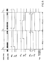
- FIG. 5 shows the timing of the signals for three lines or rows A, B, C of a display which includes display cells according to the preferred embodiment.
- the diagram of FIG. 5 is similar to that of FIG. 3 in that the rows A, B and C are rows at the top, middle and bottom of a display as shown in FIG. 1.
- the vertical sync and horizontal sync signals shown are identical to those of FIG. 3, as are the gate enable signals, again illustrated as Gate Enable A (GE A ), Gate Enable B (GE B ) and Gate Enable C (GE C ).
- the top plate voltage V TP can be changed at the same moment as the voltage applied to the liquid crystal cells LC, resulting in symmetrical signals for all elements of the display.
- the top plate voltage V TP is therefore illustrated in FIG. 5 as being changed between 0 and -30 volts, and the line outputs again vary between 0 and -30 volts. This operation results in a theoretical 30v RMS signal for the liquid crystal matrix or twice the RMS signal level of the prior art. Losses in the charge transferred between capacitors will reduce this range somewhat.
Landscapes
- Engineering & Computer Science (AREA)
- Chemical & Material Sciences (AREA)
- Crystallography & Structural Chemistry (AREA)
- Physics & Mathematics (AREA)
- Computer Hardware Design (AREA)
- General Physics & Mathematics (AREA)
- Theoretical Computer Science (AREA)
- Power Engineering (AREA)
- Liquid Crystal (AREA)
- Liquid Crystal Display Device Control (AREA)
- Transforming Electric Information Into Light Information (AREA)
Abstract
Claims (13)
- Afficheur à cristaux liquides comprenant plusieurs cellules d'affichage à cristaux liquides (60) ayant une électrode supérieure commune en forme de plaque et des moyens pour adresser un premier signal de commande à chaque cellule d'affichage (60), chaque cellule d'affichage (60) comprenant des moyens de mémorisation de signal (24) pour mémoriser un signal d'affichage et des premiers moyens formant commutateur (22) pour commuter le signal d'affichage vers les moyens de mémorisation (24) en réponse au premier signal de commande, caractérisé en ce que chaque cellule d'affichage à cristaux liquides (60) comprend en outre des deuxièmes moyens formant commutateur (62) pour commuter le signal d'affichage mémorisé par les moyens de mémorisation de signal (24) vers la cellule à cristaux liquides à un deuxième signal de commande, grâce à quoi les plusieurs cellules d'affichage à cristaux liquides (60) ayant une électrode supérieure commune en forme de plaque peuvent être activées simultanément par un deuxième signal de commande commun.
- Afficheur à cristaux liquides selon la revendication 1, caractérisé en ce que ledit deuxième signal de commande commun est un signal de synchronisation verticale.
- Afficheur à cristaux liquides selon la revendication 2, caractérisé en ce que plusieurs desdits deuxièmes moyens formant commutateur (62) sont reliés à une ligne de signal de commande commune (64) pour fournir ledit deuxième signal de commande commun.
- Afficheur à cristaux liquides selon l'une des revendications 1 à 3, caractérisé en ce que les premiers moyens formant commutateur (22) sont constitués par un premier transistor ayant une source connectée pour recevoir le signal d'affichage, un drain relié aux moyens de mémorisation de signal (24), et une grille connectée pour recevoir le premier signal de commande.
- Afficheur à cristaux liquides selon l'une des revendications précédentes, caractérisé en ce que les deuxièmes moyens de commutation (62) sont constitués par un deuxième transistor ayant une source reliée aux moyens de mémorisation de signal (24), un drain relié à la cellule à cristaux liquides, et une grille connectée pour recevoir le deuxième signal de commande.
- Afficheur à cristaux liquides selon la revendication 4 ou 5, caractérisé en ce que le premier et/ou le deuxième transistor est un transistor MOS (de "metal oxide silicon").
- Afficheur à cristaux liquides selon l'une des revendications précédentes, caractérisé en ce que les moyens de mémorisation de signal (24) sont constitués par un condensateur.
- Afficheur à cristaux liquides selon l'une des revendications précédentes, caractérisé en ce que toutes les cellules d'affichage à cristaux liquides (60) se partagent une électrode supérieure commune en forme de plaque.
- Afficheur à cristaux liquides selon l'une des revendications précédentes, caractérisé en ce que des moyens sont prévus pour fournir une tension de plaque supérieure à l'électrode supérieure commune en forme de plaque et pour alterner la tension de plaque supérieure entre des premier et deuxièmes niveaux de tension.
- Afficheur à cristaux liquides selon la revendication 9, caractérisé en ce que les moyens pour fournir la tension de plaque supérieure sont adaptés pour alterner la tension de plaque supérieure en synchronisme avec le deuxième signal de commande commun.
- Procédé pour commander un afficheur à cristaux liquides selon l'une des revendications précédentes, caractérisé en ce qu'il comprend les étapes consistant à:- mémoriser des signaux d'affichage dans les moyens de mémorisation de signal (24) des plusieurs cellules d'affichage à cristaux liquides (60); et- appliquer simultanément un deuxième signal de commande commun aux deuxièmes moyens formant commutateur (62) des plusieurs cellules d'affichage à cristaux liquides (60);
- Procédé pour commander un afficheur à cristaux liquides selon la revendication 1, caractérisé en ce qu'une tension est fournie à l'électrode supérieure commune en forme de plaque en synchronisme avec ledit deuxième signal de commande commun.
- Procédé de commande d'un afficheur à cristaux liquides selon la revendication 12, caractérisé en ce que plusieurs ensembles de signaux d'affichage sont successivement mémorisé et successivement appliqués, chaque ensemble étant appliqué en réponse à un signal respectif d'une suite de deuxièmes signaux de commande communs, et en ce que la tension appliquée à l'électrode supérieure commune en forme de plaque est successivement alternée en synchronisme avec la suite de deuxièmes signaux de commande commun.
Applications Claiming Priority (2)
| Application Number | Priority Date | Filing Date | Title |
|---|---|---|---|
| US90189 | 1987-08-27 | ||
| US07/090,189 US4870396A (en) | 1987-08-27 | 1987-08-27 | AC activated liquid crystal display cell employing dual switching devices |
Publications (2)
| Publication Number | Publication Date |
|---|---|
| EP0328633A1 EP0328633A1 (fr) | 1989-08-23 |
| EP0328633B1 true EP0328633B1 (fr) | 1992-09-30 |
Family
ID=22221697
Family Applications (1)
| Application Number | Title | Priority Date | Filing Date |
|---|---|---|---|
| EP88908540A Expired - Lifetime EP0328633B1 (fr) | 1987-08-27 | 1988-08-23 | Cellule matricielle active pour fonctionnement en courant alternatif |
Country Status (5)
| Country | Link |
|---|---|
| US (1) | US4870396A (fr) |
| EP (1) | EP0328633B1 (fr) |
| JP (1) | JP2528957B2 (fr) |
| DE (1) | DE3875104T2 (fr) |
| WO (1) | WO1989002144A1 (fr) |
Families Citing this family (66)
| Publication number | Priority date | Publication date | Assignee | Title |
|---|---|---|---|---|
| KR100202246B1 (ko) * | 1989-02-27 | 1999-06-15 | 윌리엄 비. 켐플러 | 디지탈화 비디오 시스템을 위한 장치 및 방법 |
| US5206629A (en) * | 1989-02-27 | 1993-04-27 | Texas Instruments Incorporated | Spatial light modulator and memory for digitized video display |
| US5214420A (en) * | 1989-02-27 | 1993-05-25 | Texas Instruments Incorporated | Spatial light modulator projection system with random polarity light |
| US5194974A (en) * | 1989-08-21 | 1993-03-16 | Sharp Kabushiki Kaisha | Non-flicker liquid crystal display with capacitive charge storage |
| US5225823A (en) * | 1990-12-04 | 1993-07-06 | Harris Corporation | Field sequential liquid crystal display with memory integrated within the liquid crystal panel |
| JP2775040B2 (ja) * | 1991-10-29 | 1998-07-09 | 株式会社 半導体エネルギー研究所 | 電気光学表示装置およびその駆動方法 |
| JP2798540B2 (ja) * | 1992-01-21 | 1998-09-17 | シャープ株式会社 | アクティブマトリクス基板とその駆動方法 |
| US5325106A (en) * | 1992-01-27 | 1994-06-28 | Northrop Corporation | Analog driver for scrollable spatial light modulator |
| US5257103A (en) * | 1992-02-05 | 1993-10-26 | Nview Corporation | Method and apparatus for deinterlacing video inputs |
| US6511187B1 (en) | 1992-02-20 | 2003-01-28 | Kopin Corporation | Method of fabricating a matrix display system |
| US5627557A (en) * | 1992-08-20 | 1997-05-06 | Sharp Kabushiki Kaisha | Display apparatus |
| GB9223697D0 (en) * | 1992-11-12 | 1992-12-23 | Philips Electronics Uk Ltd | Active matrix display devices |
| US5583534A (en) * | 1993-02-18 | 1996-12-10 | Canon Kabushiki Kaisha | Method and apparatus for driving liquid crystal display having memory effect |
| JPH06289817A (ja) * | 1993-04-01 | 1994-10-18 | Sharp Corp | 表示装置の駆動方法及び駆動回路 |
| JPH06317807A (ja) * | 1993-05-06 | 1994-11-15 | Sharp Corp | マトリクス表示装置およびその駆動方法 |
| JP3102666B2 (ja) * | 1993-06-28 | 2000-10-23 | シャープ株式会社 | 画像表示装置 |
| TW356546B (en) | 1993-08-10 | 1999-04-21 | Sharp Kk | An image display apparatus and a method for driving the same |
| US6448944B2 (en) | 1993-10-22 | 2002-09-10 | Kopin Corporation | Head-mounted matrix display |
| US5815126A (en) | 1993-10-22 | 1998-09-29 | Kopin Corporation | Monocular portable communication and display system |
| US7310072B2 (en) | 1993-10-22 | 2007-12-18 | Kopin Corporation | Portable communication display device |
| US5844538A (en) * | 1993-12-28 | 1998-12-01 | Sharp Kabushiki Kaisha | Active matrix-type image display apparatus controlling writing of display data with respect to picture elements |
| US5666130A (en) * | 1994-08-10 | 1997-09-09 | Hughes Aircraft Company | Point addressable display assembly, method of operating same, and method of fabricating same |
| JP3187254B2 (ja) * | 1994-09-08 | 2001-07-11 | シャープ株式会社 | 画像表示装置 |
| JP3471928B2 (ja) * | 1994-10-07 | 2003-12-02 | 株式会社半導体エネルギー研究所 | アクティブマトリクス表示装置の駆動方法 |
| US5604510A (en) * | 1995-01-10 | 1997-02-18 | Palomar Technologies Corporation | Liquid crystal display drive with voltage translation |
| US5644340A (en) * | 1995-03-16 | 1997-07-01 | Harney; Michael | Frequency mixing for controlling individual pixels in a display |
| US5767828A (en) * | 1995-07-20 | 1998-06-16 | The Regents Of The University Of Colorado | Method and apparatus for displaying grey-scale or color images from binary images |
| US5959598A (en) | 1995-07-20 | 1999-09-28 | The Regents Of The University Of Colorado | Pixel buffer circuits for implementing improved methods of displaying grey-scale or color images |
| US6181311B1 (en) * | 1996-02-23 | 2001-01-30 | Canon Kabushiki Kaisha | Liquid crystal color display apparatus and driving method thereof |
| WO1997032297A1 (fr) * | 1996-02-27 | 1997-09-04 | The Penn State Research Foundation | Procede et systeme pour la reduction du courant a l'etat bloque dans des transistors a effet de champ |
| EP0797182A1 (fr) * | 1996-03-19 | 1997-09-24 | Hitachi, Ltd. | Affichage à cristaux liquides avec matrice active et circuit de maintien de données dans chaque pixel |
| US6011530A (en) * | 1996-04-12 | 2000-01-04 | Frontec Incorporated | Liquid crystal display |
| JP3468986B2 (ja) * | 1996-04-16 | 2003-11-25 | 株式会社半導体エネルギー研究所 | アクティブマトリクス回路および表示装置 |
| US6057820A (en) * | 1996-10-21 | 2000-05-02 | Spatialight, Inc. | Apparatus and method for controlling contrast in a dot-matrix liquid crystal display |
| US6078303A (en) * | 1996-12-19 | 2000-06-20 | Colorado Microdisplay, Inc. | Display system having electrode modulation to alter a state of an electro-optic layer |
| US6046716A (en) | 1996-12-19 | 2000-04-04 | Colorado Microdisplay, Inc. | Display system having electrode modulation to alter a state of an electro-optic layer |
| US7304632B2 (en) * | 1997-05-13 | 2007-12-04 | Oki Electric Industry Co., Ltd. | Liquid-crystal display driving circuit and method |
| JPH1130975A (ja) * | 1997-05-13 | 1999-02-02 | Oki Electric Ind Co Ltd | 液晶表示装置の駆動回路及びその駆動方法 |
| US20030179168A1 (en) * | 1997-12-18 | 2003-09-25 | Scott A. Rosenberg | Voltage signal modulation scheme |
| US6310594B1 (en) * | 1998-11-04 | 2001-10-30 | International Business Machines Corporation | Driving method and circuit for pixel multiplexing circuits |
| US6476787B1 (en) * | 1998-11-04 | 2002-11-05 | International Business Machines Corporation | Multiplexing pixel circuits |
| JP2001117534A (ja) * | 1999-10-21 | 2001-04-27 | Pioneer Electronic Corp | アクティブマトリクス型表示装置及びその駆動方法 |
| US6476785B1 (en) | 1999-11-08 | 2002-11-05 | Atmel Corporation | Drive circuit for liquid crystal display cell |
| JP4123711B2 (ja) * | 2000-07-24 | 2008-07-23 | セイコーエプソン株式会社 | 電気光学パネルの駆動方法、電気光学装置、および電子機器 |
| JP3982992B2 (ja) * | 2000-12-07 | 2007-09-26 | 三洋電機株式会社 | アクティブマトリクス型表示装置 |
| US7230597B2 (en) * | 2001-07-13 | 2007-06-12 | Tpo Hong Kong Holding Limited | Active matrix array devices |
| JP4085369B2 (ja) | 2002-10-10 | 2008-05-14 | 日本ビクター株式会社 | 液晶表示装置 |
| CN100435201C (zh) * | 2002-11-15 | 2008-11-19 | 奇景光电股份有限公司 | 液晶单元结构的驱动电路及其控制方法 |
| KR100762026B1 (ko) * | 2003-03-31 | 2007-09-28 | 비오이 하이디스 테크놀로지 주식회사 | 액정표시장치 |
| JP4560275B2 (ja) * | 2003-04-04 | 2010-10-13 | 株式会社半導体エネルギー研究所 | アクティブマトリクス型表示装置とその駆動方法 |
| US20040222953A1 (en) * | 2003-05-06 | 2004-11-11 | Smith Joseph T. | Low voltage frame buffer for high contrast LCD microdisplay and method therefor |
| TW200614143A (en) * | 2004-10-19 | 2006-05-01 | Ind Tech Res Inst | Pixel equivalent circuit and method for improving the hold type of pixels |
| US7746294B2 (en) | 2006-04-14 | 2010-06-29 | University Of Central Florida Research Foundation, Inc. | Transflective liquid crystal display |
| EP2008264B1 (fr) * | 2006-04-19 | 2016-11-16 | Ignis Innovation Inc. | Plan de commande stable pour des affichages à matrice active |
| JP4508166B2 (ja) * | 2006-07-04 | 2010-07-21 | セイコーエプソン株式会社 | 表示装置およびそれを用いた表示システム |
| DK2102848T3 (en) * | 2006-12-01 | 2017-12-04 | Ses-Imagotag | Active matrix display with low power consumption |
| US7589808B2 (en) * | 2007-06-15 | 2009-09-15 | University Of Central Florida Research Foundation, Inc. | Wide viewing angle transflective liquid crystal displays |
| US20080309854A1 (en) * | 2007-06-15 | 2008-12-18 | Zhibing Ge | Wide Viewing Angle and Broadband Circular Polarizers for Transflective Liquid Crystal Displays |
| US7605897B2 (en) * | 2007-07-20 | 2009-10-20 | University Of Central Florida Research Foundation Inc. | Multi-domain vertical alignment liquid crystal displays with improved angular dependent gamma curves |
| JP5200209B2 (ja) * | 2007-08-08 | 2013-06-05 | エプソンイメージングデバイス株式会社 | 液晶表示装置 |
| US7583439B2 (en) * | 2007-08-09 | 2009-09-01 | University Of Central Florida Research Foundation, Inc. | Wide-angle and broadband polarization converter |
| US7796201B2 (en) * | 2008-03-17 | 2010-09-14 | Himax Display, Inc. | Pixel device having a capacitor comprising metal layers and a capacitor having poly-silicon layers |
| CN102023434B (zh) * | 2009-09-18 | 2013-01-23 | 北京京东方光电科技有限公司 | 阵列基板及其驱动方法 |
| WO2011104965A1 (fr) * | 2010-02-24 | 2011-09-01 | シャープ株式会社 | Dispositif et système d'affichage d'image tridimensionnelle et procédé d'entraînement de dispositif d'affichage d'image tridimensionnelle |
| US9013562B2 (en) * | 2010-06-18 | 2015-04-21 | Honeywell International Inc. | Methods and systems for presenting sequential video frames |
| CN102736290A (zh) * | 2011-04-14 | 2012-10-17 | 京东方科技集团股份有限公司 | 一种场扫描的方法和像素结构、阵列基板和显示装置 |
Family Cites Families (19)
| Publication number | Priority date | Publication date | Assignee | Title |
|---|---|---|---|---|
| US3862360A (en) * | 1973-04-18 | 1975-01-21 | Hughes Aircraft Co | Liquid crystal display system with integrated signal storage circuitry |
| JPS5911916B2 (ja) * | 1976-05-25 | 1984-03-19 | 株式会社日立製作所 | 表示デ−タ合成回路 |
| US4114070A (en) * | 1977-03-22 | 1978-09-12 | Westinghouse Electric Corp. | Display panel with simplified thin film interconnect system |
| US4335936A (en) * | 1977-10-14 | 1982-06-22 | Sharp Kabushiki Kaisha | Matrix electrode structure in a multi-layer matrix type liquid crystal display |
| JPS5458399A (en) * | 1977-10-18 | 1979-05-11 | Sharp Corp | Matrix type liquid crystal display unit |
| GB2034953B (en) * | 1978-10-25 | 1982-10-27 | Sharp Kk Mos Fet | Array drive for liquid crystal matrix display |
| JPS55159493A (en) * | 1979-05-30 | 1980-12-11 | Suwa Seikosha Kk | Liquid crystal face iimage display unit |
| DE3176454D1 (en) * | 1980-02-22 | 1987-10-22 | Toshiba Kk | Liquid crystal display device |
| JPS5741078A (en) * | 1980-08-22 | 1982-03-06 | Seiko Epson Corp | Synchronizing circuit of matrix television |
| JPS5799688A (en) * | 1980-12-11 | 1982-06-21 | Sharp Kk | Display driving circuit |
| JPS57120992A (en) * | 1981-01-21 | 1982-07-28 | Seiko Instr & Electronics | Picture display device |
| US4455576A (en) * | 1981-04-07 | 1984-06-19 | Seiko Instruments & Electronics Ltd. | Picture display device |
| FR2524679B1 (fr) * | 1982-04-01 | 1990-07-06 | Suwa Seikosha Kk | Procede d'attaque d'un panneau d'affichage a cristaux liquides a matrice active |
| JPS59123884A (ja) * | 1982-12-29 | 1984-07-17 | シャープ株式会社 | 液晶表示装置の駆動方法 |
| JPS6059389A (ja) * | 1983-09-12 | 1985-04-05 | シャープ株式会社 | 液晶表示装置の駆動回路 |
| JPS6083477A (ja) * | 1983-10-13 | 1985-05-11 | Sharp Corp | 液昇表示装置の駆動回路 |
| JPS60257683A (ja) * | 1984-06-01 | 1985-12-19 | Sharp Corp | 液晶表示装置の駆動回路 |
| JPS61267734A (ja) * | 1985-05-23 | 1986-11-27 | Seiko Epson Corp | 液晶電気光学装置 |
| JPS61290490A (ja) * | 1985-06-18 | 1986-12-20 | 三菱電機株式会社 | マトリクス形表示素子 |
-
1987
- 1987-08-27 US US07/090,189 patent/US4870396A/en not_active Expired - Fee Related
-
1988
- 1988-08-23 WO PCT/US1988/002926 patent/WO1989002144A1/fr not_active Ceased
- 1988-08-23 JP JP63507802A patent/JP2528957B2/ja not_active Expired - Lifetime
- 1988-08-23 EP EP88908540A patent/EP0328633B1/fr not_active Expired - Lifetime
- 1988-08-23 DE DE8888908540T patent/DE3875104T2/de not_active Expired - Fee Related
Non-Patent Citations (1)
| Title |
|---|
| Patent Abstracts of Japan, Vol. 8, No. 192 (P-298), Abstract of JP 59-81621 published 1984-05-11 * |
Also Published As
| Publication number | Publication date |
|---|---|
| JP2528957B2 (ja) | 1996-08-28 |
| US4870396A (en) | 1989-09-26 |
| JPH02500621A (ja) | 1990-03-01 |
| EP0328633A1 (fr) | 1989-08-23 |
| DE3875104D1 (de) | 1992-11-05 |
| DE3875104T2 (de) | 1993-04-08 |
| WO1989002144A1 (fr) | 1989-03-09 |
Similar Documents
| Publication | Publication Date | Title |
|---|---|---|
| US4870396A (en) | AC activated liquid crystal display cell employing dual switching devices | |
| US4845482A (en) | Method for eliminating crosstalk in a thin film transistor/liquid crystal display | |
| US4804951A (en) | Display apparatus and driving method therefor | |
| KR0128729B1 (ko) | 매트릭스 표시 장치 | |
| EP0622772B1 (fr) | Méthode et dispositif pour éliminer la diaphonie dans un dispositif d'affichage à cristaux liquides à matrice active | |
| US5926158A (en) | Image display apparatus | |
| EP0216188B1 (fr) | Panneau d'affichage matriciel | |
| EP0362974B1 (fr) | Circuit de commande pour un dispositif d'affichage à matrice | |
| US6031514A (en) | Method for driving liquid crystal display device | |
| US5777591A (en) | Matrix display apparatus employing dual switching means and data signal line driving means | |
| US5898416A (en) | Display device | |
| EP0489459B1 (fr) | Méthode de commande d'un dispositif d'affichage matriciel et un dispositif d'affichage matriciel commandé par cette méthode | |
| JPS647391B2 (fr) | ||
| US5796380A (en) | Liquid crystal apparatus and method of driving same | |
| US6057820A (en) | Apparatus and method for controlling contrast in a dot-matrix liquid crystal display | |
| US5742270A (en) | Over line scan method | |
| US6703996B2 (en) | Device and method for addressing LCD pixels | |
| US20020186195A1 (en) | Electro-optic display device using a multi-row addressing scheme | |
| US20060181495A1 (en) | Active matrix array device | |
| US20020167479A1 (en) | High performance reflective liquid crystal light valve using a multi-row addressing scheme | |
| JP3297335B2 (ja) | 液晶表示装置 | |
| GB2160346A (en) | Active matrix display | |
| JP3149084B2 (ja) | 表示装置 | |
| JPS62241480A (ja) | 表示装置の駆動方法 |
Legal Events
| Date | Code | Title | Description |
|---|---|---|---|
| PUAI | Public reference made under article 153(3) epc to a published international application that has entered the european phase |
Free format text: ORIGINAL CODE: 0009012 |
|
| 17P | Request for examination filed |
Effective date: 19890421 |
|
| AK | Designated contracting states |
Kind code of ref document: A1 Designated state(s): DE FR GB NL SE |
|
| 17Q | First examination report despatched |
Effective date: 19910528 |
|
| GRAA | (expected) grant |
Free format text: ORIGINAL CODE: 0009210 |
|
| AK | Designated contracting states |
Kind code of ref document: B1 Designated state(s): DE FR GB NL SE |
|
| PG25 | Lapsed in a contracting state [announced via postgrant information from national office to epo] |
Ref country code: SE Effective date: 19920930 |
|
| REF | Corresponds to: |
Ref document number: 3875104 Country of ref document: DE Date of ref document: 19921105 |
|
| ET | Fr: translation filed | ||
| PLBE | No opposition filed within time limit |
Free format text: ORIGINAL CODE: 0009261 |
|
| STAA | Information on the status of an ep patent application or granted ep patent |
Free format text: STATUS: NO OPPOSITION FILED WITHIN TIME LIMIT |
|
| PG25 | Lapsed in a contracting state [announced via postgrant information from national office to epo] |
Ref country code: GB Effective date: 19930823 |
|
| 26N | No opposition filed | ||
| GBPC | Gb: european patent ceased through non-payment of renewal fee |
Effective date: 19930823 |
|
| PGFP | Annual fee paid to national office [announced via postgrant information from national office to epo] |
Ref country code: FR Payment date: 20000801 Year of fee payment: 13 |
|
| PGFP | Annual fee paid to national office [announced via postgrant information from national office to epo] |
Ref country code: DE Payment date: 20000802 Year of fee payment: 13 |
|
| PGFP | Annual fee paid to national office [announced via postgrant information from national office to epo] |
Ref country code: NL Payment date: 20000808 Year of fee payment: 13 |
|
| PG25 | Lapsed in a contracting state [announced via postgrant information from national office to epo] |
Ref country code: NL Free format text: LAPSE BECAUSE OF NON-PAYMENT OF DUE FEES Effective date: 20020301 |
|
| PG25 | Lapsed in a contracting state [announced via postgrant information from national office to epo] |
Ref country code: FR Free format text: LAPSE BECAUSE OF NON-PAYMENT OF DUE FEES Effective date: 20020430 |
|
| NLV4 | Nl: lapsed or anulled due to non-payment of the annual fee |
Effective date: 20020301 |
|
| PG25 | Lapsed in a contracting state [announced via postgrant information from national office to epo] |
Ref country code: DE Free format text: LAPSE BECAUSE OF NON-PAYMENT OF DUE FEES Effective date: 20020501 |
|
| REG | Reference to a national code |
Ref country code: FR Ref legal event code: ST |