EP0328899A2 - Verfahren und Schaltung zur Paritätserzeugung - Google Patents
Verfahren und Schaltung zur Paritätserzeugung Download PDFInfo
- Publication number
- EP0328899A2 EP0328899A2 EP89101069A EP89101069A EP0328899A2 EP 0328899 A2 EP0328899 A2 EP 0328899A2 EP 89101069 A EP89101069 A EP 89101069A EP 89101069 A EP89101069 A EP 89101069A EP 0328899 A2 EP0328899 A2 EP 0328899A2
- Authority
- EP
- European Patent Office
- Prior art keywords
- bit
- parity
- sum
- output
- adder
- Prior art date
- Legal status (The legal status is an assumption and is not a legal conclusion. Google has not performed a legal analysis and makes no representation as to the accuracy of the status listed.)
- Withdrawn
Links
Images




Classifications
-
- G—PHYSICS
- G06—COMPUTING OR CALCULATING; COUNTING
- G06F—ELECTRIC DIGITAL DATA PROCESSING
- G06F11/00—Error detection; Error correction; Monitoring
- G06F11/07—Responding to the occurrence of a fault, e.g. fault tolerance
- G06F11/08—Error detection or correction by redundancy in data representation, e.g. by using checking codes
- G06F11/10—Adding special bits or symbols to the coded information, e.g. parity check, casting out 9's or 11's
-
- G—PHYSICS
- G06—COMPUTING OR CALCULATING; COUNTING
- G06F—ELECTRIC DIGITAL DATA PROCESSING
- G06F7/00—Methods or arrangements for processing data by operating upon the order or content of the data handled
- G06F7/38—Methods or arrangements for performing computations using exclusively denominational number representation, e.g. using binary, ternary, decimal representation
- G06F7/48—Methods or arrangements for performing computations using exclusively denominational number representation, e.g. using binary, ternary, decimal representation using non-contact-making devices, e.g. tube, solid state device; using unspecified devices
- G06F7/50—Adding; Subtracting
- G06F7/505—Adding; Subtracting in bit-parallel fashion, i.e. having a different digit-handling circuit for each denomination
- G06F7/506—Adding; Subtracting in bit-parallel fashion, i.e. having a different digit-handling circuit for each denomination with simultaneous carry generation for, or propagation over, two or more stages
Definitions
- the invention relates to a data processing technology and more particularly relates to arithmetic circuitry and a method especially for the generation of parity bit values.
- parity bit to be associated with a byte or multiple byte expression of a numeric value is well-known in the art, and is used as a means to insure that single bit errors which occur in the byte or multiple byte expression can be detected and with appropriate circuitry, corrected.
- the production of a parity bit finds its best use in the detection of errors which occur during the transmission of a byte or multiple byte expression over a communications medium.
- parity can be considered as either even parity or odd parity.
- Odd parity is defined herein as a binary bit P having a value of one when the byte or multiple byte expression with which it is associated has an odd number of ones contained therein.
- odd parity will be employed as the form of parity to be discussed. The choice of even or odd parity is merely a local convention, either choice providing essentially the same results.
- the classic technique for generating the parity of a sum output of an N bit adder is to apply the N bits of the sum output to an N bit exclusive OR (in reality an exclusive OR tree) so as to produce a single binary bit for the odd parity value associated with the N bit sum.
- the problem in the prior art of producing parity in this classical manner is the duration required, since one must wait for the carry bit to propagate over all of the N bits producing the N bit sum, in order to be able to apply all N bits to the N bit input of the exclusive OR parity generator.
- a number of techniques have been attempted in the prior art to reduce the duration necessary to compute the parity of the sum output of an N bit adder.
- the parity generation circuit which is disclosed takes advantage of a property of the parity of a number before and after it has been incremented. This is characterized as the parity toggle property and it allows parity generation to be done on the most significant bits of an adder before the carry input to these most significant bits has been generated from the least significant bit portion of the sum produced by the adder. The final parity for the entire sum output of the addition process is adjusted quickly when the carry into the most significant bits of the sum becomes available from the least significant bit portion of the sum output.
- the parity toggle property of the invention allows for the quick adjustment of the parity without incurring the undue delay of waiting for the production of the carry output from the low order sum before commencing computations with the high order sum.
- FIG. 1 The principle of operation of the invention is set forth in the table of Fig. 2 and is further described in the functional block diagram of Fig. 1.
- the improved parity generator for the sum output of an adder is shown in Fig. 1.
- First input operand A has M high order bits AH and N low order bits AL applied to a first register 10 in Fig. 1.
- a second input operand B has M high order bits BH and N low order bits BL applied to the input register 12.
- the operands A and B are to be added in a two input adder associated with the parity generator circuit. The sum of that addition is to have its parity established and that is the objective of the improved parity generator invention.
- the parity generator circuit of Fig. 1 has a first M bit adder 14 which receives a first M bit operand AH and a second M bit operand BH from the registers 10 and 12 of Fig. 1, and the adder 14 produces an M bit high order sum SH′ without carry.
- the adder 14 will not use a carry input. Therefore, any existing adder circuit which is used to implement adder 14 must have its carry input terminal disabled, usually by connecting it to a logical zero.
- a first parity generator 16 of Fig. 1 is connected to the sum output of the M bit adder 14, for producing a high order parity bit without carry PH′.
- a parity toggle means 18 is shown in Fig. 1.
- the parity toggle means 18 can be a random access memory (RAM) or read only memory (ROM) or a program logic array (PLA) or a complex logic function which carries out the parity toggle operation.
- the parity toggle mechanism 18 has an input connected to the sum output of the M bit adder 14, for producing a parity toggle bit having a binary value of one if there are an even number of binary ones to the right of the first binary zero in the sum output of the M bit adder 14. Alternately, the parity toggle bit produced by the parity toggle means 18 will have a binary value of zero if there are an odd number of binary ones to the right of the first binary zero in the sum output of the M bit adder 14.
- An M bit register 15 is shown between the sum output of the adder 14 and the parity generator 16 and the parity toggle means 18, and is used for the purpose of temporarily storing the sum output from the adder 14.
- the improved parity generator of Fig. 1 further includes an N bit adder 20 having an N bit value AL applied as a first operand input thereto and having an N bit value BL applied as a second operand input thereto from the registers 10 and 12 of Fig. 1.
- the adder 20 produces an N bit low order sum SL and a low order carry bit CL.
- An N bit register 21 is connected to the sum output of the adder 20, for temporarily storing the sum value output from the adder 20.
- the single bit register 23 connected to the low order carry bit output of the adder 20 will provide a similar temporary storage for CL.
- a second parity generator 22 shown in Fig. 1 has its input connected through the register 21 to the sum output of the N bit adder 20, for producing a low order parity bit PL.
- An AND gate 24 has a first input connected to the parity toggle bit output from the parity means 18 and it has a second input connected, through register 23, to the low order carry bit CL output from the N bit adder 20, and it has an output.
- a three input exclusive OR 26 is shown in Fig. 1 which has a first input connected to the output of the AND gate 24, a second input connected to the high order parity without carry bit PH′ from the first parity generator 16, and it has a third input connected from the low order parity bit PL of the second parity generator 22.
- the output of the three input exclusive OR 26 is the parity PS of the sum of the operands A and B.
- the registers 10 and 12 of Fig. 1 could be eliminated and the inputs A and B directly applied to the adders 14 and 20.
- the registers 15, 21 and 23 could be eliminated in Fig. 1.
- the AND gate 24 and exclusive OR 26 perform a compound logical operation of combining the four inputs Ptog, PH′, CL and PL by ANDing and exclusive ORing these binary values to obtain PS, as described. There are many other combinations of elementary logic elements which can be combined to accomplish this compound logical operation.
- parity generator 16 were instead, an even parity generator, then it would output the complement binary value (not PH′), which can be logically compensated for by an inversion or an equivalent logical operation.
- parity generator 22 if it employed even parity, instead of the odd parity disclosed for the specific embodiment.
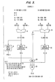
- Fig. 3 is an example of the operation of the invention for 16 bit operands A and B.
- Fig. 3 further shows the binary values for AH and BH being applied to the adder 14 producing the sum output SH′ which is applied to the parity toggle means 18 and the parity generator 16.
- the carry output CL from the adder 20 is applied to one of the inputs of the AND gate 24.
- the output of the AND gate 24 is applied to the third input of the exclusive OR 26.
- Fig. 4 and Fig. 5 provide an example of the generation of the parity for the sum of two 6 bit operands, where the partitioning of the operands is changed from odd to even, in order to further illustrate the invention.
- the operands A and B in example 2A of Fig. 4 are the same as the operands A and B of the example 2B of Fig. 5.
- the value M for the number of bits in AH and BH is an odd value
- the value of M in Fig. 5 is an even value.
- the parity toggle means 18 generates a value of Ptog of 1, a value for the parity PH′ of 0, a value for CL of 1 and a value of PL of 1.
Landscapes
- Engineering & Computer Science (AREA)
- Theoretical Computer Science (AREA)
- Quality & Reliability (AREA)
- Physics & Mathematics (AREA)
- General Engineering & Computer Science (AREA)
- General Physics & Mathematics (AREA)
- Error Detection And Correction (AREA)
- Detection And Correction Of Errors (AREA)
Applications Claiming Priority (2)
| Application Number | Priority Date | Filing Date | Title |
|---|---|---|---|
| US07/156,626 US4879675A (en) | 1988-02-17 | 1988-02-17 | Parity generator circuit and method |
| US156626 | 1988-02-17 |
Publications (2)
| Publication Number | Publication Date |
|---|---|
| EP0328899A2 true EP0328899A2 (de) | 1989-08-23 |
| EP0328899A3 EP0328899A3 (de) | 1991-09-11 |
Family
ID=22560357
Family Applications (1)
| Application Number | Title | Priority Date | Filing Date |
|---|---|---|---|
| EP19890101069 Withdrawn EP0328899A3 (de) | 1988-02-17 | 1989-01-23 | Verfahren und Schaltung zur Paritätserzeugung |
Country Status (3)
| Country | Link |
|---|---|
| US (1) | US4879675A (de) |
| EP (1) | EP0328899A3 (de) |
| JP (1) | JPH01220528A (de) |
Families Citing this family (6)
| Publication number | Priority date | Publication date | Assignee | Title |
|---|---|---|---|---|
| US5557622A (en) * | 1990-10-01 | 1996-09-17 | Digital Equipment Corporation | Method and apparatus for parity generation |
| US5608741A (en) * | 1993-11-23 | 1997-03-04 | Intel Corporation | Fast parity generator using complement pass-transistor logic |
| FR2713364B1 (fr) * | 1993-11-30 | 1996-01-12 | Bull Sa | Dispositif de calcul des bits de parité associés à une somme de deux nombres. |
| US5825204A (en) * | 1996-03-21 | 1998-10-20 | Hashimoto; Masashi | Apparatus and method for a party check logic circuit in a dynamic random access memory |
| KR100224278B1 (ko) * | 1996-12-18 | 1999-10-15 | 윤종용 | 패스 트랜지스터 로직을 사용하는 조건 합 가산기 및 그것을 구비한 집적 회로 |
| US6990507B2 (en) * | 2002-05-21 | 2006-01-24 | Hewlett-Packard Development Company, L.P. | Parity prediction for arithmetic increment function |
Family Cites Families (9)
| Publication number | Priority date | Publication date | Assignee | Title |
|---|---|---|---|---|
| US3222652A (en) * | 1961-08-07 | 1965-12-07 | Ibm | Special-function data processing |
| US3287546A (en) * | 1963-02-27 | 1966-11-22 | Ibm | Parity prediction apparatus for use with a binary adder |
| GB1047246A (de) * | 1963-02-27 | |||
| US3342983A (en) * | 1963-06-25 | 1967-09-19 | Ibm | Parity checking and parity generating means for binary adders |
| US3596072A (en) * | 1968-05-24 | 1971-07-27 | Hitachi Ltd | Error-detecting circuitry in adder system |
| US3758760A (en) * | 1972-04-07 | 1973-09-11 | Honeywell Inf Systems | Error detection for arithmetic and logical unit modules |
| US3925647A (en) * | 1974-09-30 | 1975-12-09 | Honeywell Inf Systems | Parity predicting and checking logic for carry look-ahead binary adder |
| US4224680A (en) * | 1978-06-05 | 1980-09-23 | Fujitsu Limited | Parity prediction circuit for adder/counter |
| US4608693A (en) * | 1984-05-07 | 1986-08-26 | At&T Bell Laboratories | Fault detection arrangement for a digital conferencing system |
-
1988
- 1988-02-17 US US07/156,626 patent/US4879675A/en not_active Expired - Fee Related
- 1988-11-18 JP JP63290385A patent/JPH01220528A/ja active Granted
-
1989
- 1989-01-23 EP EP19890101069 patent/EP0328899A3/de not_active Withdrawn
Also Published As
| Publication number | Publication date |
|---|---|
| EP0328899A3 (de) | 1991-09-11 |
| JPH01220528A (ja) | 1989-09-04 |
| US4879675A (en) | 1989-11-07 |
| JPH0370416B2 (de) | 1991-11-07 |
Similar Documents
| Publication | Publication Date | Title |
|---|---|---|
| US4682303A (en) | Parallel binary adder | |
| US4616330A (en) | Pipelined multiply-accumulate unit | |
| US5764554A (en) | Method for the implementation of modular reduction according to the Montgomery method | |
| US4953115A (en) | Absolute value calculating circuit having a single adder | |
| US5367477A (en) | Method and apparatus for performing parallel zero detection in a data processing system | |
| EP1752870B1 (de) | Multiplizierer | |
| US5805491A (en) | Fast 4-2 carry save adder using multiplexer logic | |
| US6175852B1 (en) | High-speed binary adder | |
| GB2232280A (en) | Evaluation of an extremum of binary encoded words | |
| US5177703A (en) | Division circuit using higher radices | |
| US4879675A (en) | Parity generator circuit and method | |
| JPH0545982B2 (de) | ||
| US4901269A (en) | Multiple-stage carry-select adder having unique construction for initial adder cells | |
| US6519621B1 (en) | Arithmetic circuit for accumulative operation | |
| US3842250A (en) | Circuit for implementing rounding in add/subtract logic networks | |
| EP0605885A2 (de) | Verfahren und Gerät zum automatischen Entwurf logischer Schaltung und Multiplikator | |
| US6163790A (en) | Modular arithmetic coprocessor comprising an integer division circuit | |
| EP0512686B1 (de) | Abrundungsschaltung in einem Gleitkommamultiplizierer | |
| JPS6238975A (ja) | 自己相関装置 | |
| US4538237A (en) | Method and apparatus for calculating the residue of a binary number | |
| KR0147942B1 (ko) | 승산기에서의 부스 레코딩회로 | |
| US4506340A (en) | Method and apparatus for producing the residue of the product of two residues | |
| US12135955B2 (en) | Systems and methods for low latency modular multiplication | |
| JPH05197525A (ja) | オペランドを否定するための否定方法及び否定回路 | |
| JP2991788B2 (ja) | 復号器 |
Legal Events
| Date | Code | Title | Description |
|---|---|---|---|
| PUAI | Public reference made under article 153(3) epc to a published international application that has entered the european phase |
Free format text: ORIGINAL CODE: 0009012 |
|
| AK | Designated contracting states |
Kind code of ref document: A2 Designated state(s): DE FR GB |
|
| 17P | Request for examination filed |
Effective date: 19891214 |
|
| PUAL | Search report despatched |
Free format text: ORIGINAL CODE: 0009013 |
|
| AK | Designated contracting states |
Kind code of ref document: A3 Designated state(s): DE FR GB |
|
| STAA | Information on the status of an ep patent application or granted ep patent |
Free format text: STATUS: THE APPLICATION IS DEEMED TO BE WITHDRAWN |
|
| 18D | Application deemed to be withdrawn |
Effective date: 19940801 |
|
| R18D | Application deemed to be withdrawn (corrected) |
Effective date: 19940802 |