EP0329227A1 - Verfahren zum Herstellen einer Halbleiteranordnung - Google Patents
Verfahren zum Herstellen einer Halbleiteranordnung Download PDFInfo
- Publication number
- EP0329227A1 EP0329227A1 EP89200300A EP89200300A EP0329227A1 EP 0329227 A1 EP0329227 A1 EP 0329227A1 EP 89200300 A EP89200300 A EP 89200300A EP 89200300 A EP89200300 A EP 89200300A EP 0329227 A1 EP0329227 A1 EP 0329227A1
- Authority
- EP
- European Patent Office
- Prior art keywords
- nitrogen
- titanium
- layer
- titanium layer
- silicon
- Prior art date
- Legal status (The legal status is an assumption and is not a legal conclusion. Google has not performed a legal analysis and makes no representation as to the accuracy of the status listed.)
- Withdrawn
Links
Images
Classifications
-
- H—ELECTRICITY
- H10—SEMICONDUCTOR DEVICES; ELECTRIC SOLID-STATE DEVICES NOT OTHERWISE PROVIDED FOR
- H10P—GENERIC PROCESSES OR APPARATUS FOR THE MANUFACTURE OR TREATMENT OF DEVICES COVERED BY CLASS H10
- H10P14/00—Formation of materials, e.g. in the shape of layers or pillars
- H10P14/40—Formation of materials, e.g. in the shape of layers or pillars of conductive or resistive materials
- H10P14/418—Formation of materials, e.g. in the shape of layers or pillars of conductive or resistive materials the conductive layers comprising transition metals
-
- H—ELECTRICITY
- H10—SEMICONDUCTOR DEVICES; ELECTRIC SOLID-STATE DEVICES NOT OTHERWISE PROVIDED FOR
- H10P—GENERIC PROCESSES OR APPARATUS FOR THE MANUFACTURE OR TREATMENT OF DEVICES COVERED BY CLASS H10
- H10P14/00—Formation of materials, e.g. in the shape of layers or pillars
- H10P14/60—Formation of materials, e.g. in the shape of layers or pillars of insulating materials
- H10P14/63—Formation of materials, e.g. in the shape of layers or pillars of insulating materials characterised by the formation processes
- H10P14/6302—Non-deposition formation processes
- H10P14/6316—Formation by nitridation, e.g. nitridation of the substrate
-
- H—ELECTRICITY
- H10—SEMICONDUCTOR DEVICES; ELECTRIC SOLID-STATE DEVICES NOT OTHERWISE PROVIDED FOR
- H10P—GENERIC PROCESSES OR APPARATUS FOR THE MANUFACTURE OR TREATMENT OF DEVICES COVERED BY CLASS H10
- H10P14/00—Formation of materials, e.g. in the shape of layers or pillars
- H10P14/60—Formation of materials, e.g. in the shape of layers or pillars of insulating materials
- H10P14/63—Formation of materials, e.g. in the shape of layers or pillars of insulating materials characterised by the formation processes
- H10P14/6302—Non-deposition formation processes
- H10P14/6322—Formation by thermal treatments
-
- H—ELECTRICITY
- H10—SEMICONDUCTOR DEVICES; ELECTRIC SOLID-STATE DEVICES NOT OTHERWISE PROVIDED FOR
- H10P—GENERIC PROCESSES OR APPARATUS FOR THE MANUFACTURE OR TREATMENT OF DEVICES COVERED BY CLASS H10
- H10P14/00—Formation of materials, e.g. in the shape of layers or pillars
- H10P14/60—Formation of materials, e.g. in the shape of layers or pillars of insulating materials
- H10P14/69—Inorganic materials
- H10P14/692—Inorganic materials composed of oxides, glassy oxides or oxide-based glasses
- H10P14/6938—Inorganic materials composed of oxides, glassy oxides or oxide-based glasses the material containing at least one metal element, e.g. metal oxides, metal oxynitrides or metal oxycarbides
- H10P14/6939—Inorganic materials composed of oxides, glassy oxides or oxide-based glasses the material containing at least one metal element, e.g. metal oxides, metal oxynitrides or metal oxycarbides characterised by the metal
- H10P14/69394—Inorganic materials composed of oxides, glassy oxides or oxide-based glasses the material containing at least one metal element, e.g. metal oxides, metal oxynitrides or metal oxycarbides characterised by the metal the material containing titanium, e.g. TiO2
-
- H—ELECTRICITY
- H10—SEMICONDUCTOR DEVICES; ELECTRIC SOLID-STATE DEVICES NOT OTHERWISE PROVIDED FOR
- H10W—GENERIC PACKAGES, INTERCONNECTIONS, CONNECTORS OR OTHER CONSTRUCTIONAL DETAILS OF DEVICES COVERED BY CLASS H10
- H10W20/00—Interconnections in chips, wafers or substrates
- H10W20/01—Manufacture or treatment
- H10W20/031—Manufacture or treatment of conductive parts of the interconnections
Definitions
- the invention relates to a method of manufacturing a semiconductor device, in which a semiconductor body of silicon is contacted at the surface of a silicon-containing part by forming on it in order of succession a titanium layer, a nitrogen-containing titanium layer and an aluminium layer.
- the combination of the titanium and titanium nitride layers has between a silicon body and an aluminium layer a good contact resistance with the silicon and substantially no interaction with the aluminium layer.
- a combination of a titanium layer and a nitrogen-containing titanium layer is to be preferred to a titanium layer alone because, though the latter has a lower contact resistance with silicon, it is reactive with aluminium.
- a combination of a titanium layer and a nitrogen-containing titanium layer is also to be preferred to a nitrogen-containing titanium layer alone because, though the latter is less reactive with aluminium, it has a higher contact resistance with silicon.
- the titanium and titanium nitride layers are formed by sputtering.
- the titanium layer is first formed by sputtering of a thoroughly cleaned titanium target, after which in the same apparatus the titanium nitride layer is formed by sputtering of the same titanium target in a nitrogen-containing atmosphere.
- the said sputtering process has the disadvantage that it is complicated. With a clean apparatus, reasonable results can be attained when the method is carried out for the first time, but when the method is carried out for the second time, an impure titanium layer is often obtained by subsequent delivery of nitrogen still present in the apparatus after the method has been carried out for the first time.
- the deposition rate of titanium nitride also strongly decreases soon by nitridation of the titanium target.
- the invention has inter alia for its object to avoid the aforementioned disadvantages at least to a great extent.
- the invention is based inter alia on the recognition of the fact that improvements are possible by forming the nitrogen-containing titanium layer by a process other than sputtering.
- the method mentioned in the opening paragraph is therefore characterized in that the nitrogen-containing titanium layer is formed by converting titanium in a part of the titanium layer adjoining the surface in a short treatment at elevated temperature in a nitrogen-containing atmosphere into the nitrogen-containing titanium layer.
- the heat treatment is preferably carried out in 5 to 60 seconds and at a temperature of 300 - 750°C, for example by heating for 30 seconds at a temperature of 550°C and a nitrogen pressure of 1 atm.
- the titanium layer can be formed in a usual manner by sputtering.
- the titanium layer may contain additions of, for
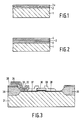
- Figure 1 and Figure 2 show diagrammatically and in sectional view a part of a semiconductor device at successive stages of manufacture by means of the method according to the invention and Figure 3 shows also diagrammatically and in sectional view another part of a semiconductor device at a stage of manufacture by means of the method according to the invention.
- Figures 1 and 2 show that in a method of manufacturing a semiconductor device a semiconductor body 1 of silicon is contacted by forming on it in order of succession a titanium layer 2, a nitrogen-containing titanium layer 3 and an aluminium layer 4.
- the nitrogen-containing titanium layer 3 is formed by converting titanium in a part 2a of the titanium layer 2 adjoining the surface in a short treatment at elevated temperature in a nitrogen-containing atmosphere into the nitrogen-containing titanium layer 3.
- the treatment is so short that the titanium substantially does not attack any underlying silicon oxide, that the titanium at most reacts partly with the underlying silicon and that substantially no oxidation of the titanium by small traces of oxygen, if any, can occur.
- a layer system of a titanium layer and a nitrogen-containing titanium layer is obtained, which has a low resistance with silicon and is substantially not reactive with aluminium.
- a consequence of the low reaction of titanium with silicon oxide in the method according to the invention is that the contacts need not be aligned accurately to the openings in oxide layers and may lie in part over silicon oxide layers present on the surface of the silicon body. .
- Figure 3 indicates how a layer system consisting of a titanium layer 32, a nitrogen-containing titanium layer 33 and an aluminium layer 34 contacts a silicon body 31 by means of the method according to the invention.
- oxide regions 35 sunken into the silicon body 31 an insulated gate electrode 36, source and drain regions 37 and 38 and an oxide layer 39 are formed in a usual manner.
- the titanium layers 2 and 32 are provided by sputtering of titanium and have a thickness of, for example, 0.1 ⁇ m.
- the semiconductor body is heated for 30 seconds at 550°C in a nitrogen atmosphere and the nitrogen-containing titanium layers 3 and 33 are formed.
- the titanium layer is then converted over approximately half its thickness.
- aluminium containing 1% of silicon is deposited in a usual manner in a thickness of about 1 ⁇ m.
- a desired pattern is then provided also in a usual manner in the aluminium layers, in the nitrogen-containing titanium layers and in the titanium layers.
- the nitrogen-containing atmosphere may be obtained by the use of nitrogen, ammonia or hydrazine as nitrogen source.
- the nitrogen or nitrogen compounds may also be rarefied by an inert gas, for example argon. It may be very useful to add besides nitrogen traces of oxygen to the atmosphere in which the heat treatment is carried out, as a result of which the reactivity of the nitrogen-containing titanium layer with aluminium is still further reduced.
- the titanium and nitrogen-containing titanium layers may also be provided on silicide layers, for example titanium or cobalt silicide layers, disposed on the silicon body.
Landscapes
- Internal Circuitry In Semiconductor Integrated Circuit Devices (AREA)
- Electrodes Of Semiconductors (AREA)
Applications Claiming Priority (2)
| Application Number | Priority Date | Filing Date | Title |
|---|---|---|---|
| NL8800359 | 1988-02-15 | ||
| NL8800359A NL8800359A (nl) | 1988-02-15 | 1988-02-15 | Werkwijze voor het vervaardigen van een halfgeleiderinrichting. |
Publications (1)
| Publication Number | Publication Date |
|---|---|
| EP0329227A1 true EP0329227A1 (de) | 1989-08-23 |
Family
ID=19851778
Family Applications (1)
| Application Number | Title | Priority Date | Filing Date |
|---|---|---|---|
| EP89200300A Withdrawn EP0329227A1 (de) | 1988-02-15 | 1989-02-09 | Verfahren zum Herstellen einer Halbleiteranordnung |
Country Status (4)
| Country | Link |
|---|---|
| EP (1) | EP0329227A1 (de) |
| JP (1) | JPH01251611A (de) |
| KR (1) | KR890013721A (de) |
| NL (1) | NL8800359A (de) |
Cited By (14)
| Publication number | Priority date | Publication date | Assignee | Title |
|---|---|---|---|---|
| EP0452921A3 (en) * | 1990-04-20 | 1992-10-28 | Applied Materials Inc. | Formation of titanium nitride on semiconductor wafer by reaction of titanium with nitrogen-bearing gas in an integrated processing system |
| EP0488628A3 (en) * | 1990-11-30 | 1992-11-04 | Sgs-Thomson Microelectronics, Inc. | Method of producing an aluminum stacked contact/via for multilayer interconnections |
| EP0525517A1 (de) * | 1991-08-02 | 1993-02-03 | Siemens Aktiengesellschaft | Verfahren zur Auffüllung mindestens eines Kontaktloches in einer isolierenden Schicht |
| EP0535354A1 (de) * | 1991-08-26 | 1993-04-07 | Motorola, Inc. | Verfahren zur Bildung einer Nitridschicht mit Benutzung von vorgewärmtem Ammoniak |
| US5374592A (en) * | 1992-09-22 | 1994-12-20 | Sgs-Thomson Microelectronics, Inc. | Method for forming an aluminum metal contact |
| US5472912A (en) * | 1989-11-30 | 1995-12-05 | Sgs-Thomson Microelectronics, Inc. | Method of making an integrated circuit structure by using a non-conductive plug |
| US5658828A (en) * | 1989-11-30 | 1997-08-19 | Sgs-Thomson Microelectronics, Inc. | Method for forming an aluminum contact through an insulating layer |
| US5930673A (en) * | 1990-11-05 | 1999-07-27 | Stmicroelectronics, Inc. | Method for forming a metal contact |
| EP1008172A4 (de) * | 1995-09-29 | 2000-06-14 | Intel Corp | Verbesserte schnittstelle zwischen titan und aluminiumlegierung in metallstapelfür integrierte schaltung |
| US6242811B1 (en) | 1989-11-30 | 2001-06-05 | Stmicroelectronics, Inc. | Interlevel contact including aluminum-refractory metal alloy formed during aluminum deposition at an elevated temperature |
| US6271137B1 (en) | 1989-11-30 | 2001-08-07 | Stmicroelectronics, Inc. | Method of producing an aluminum stacked contact/via for multilayer |
| US6287963B1 (en) | 1990-11-05 | 2001-09-11 | Stmicroelectronics, Inc. | Method for forming a metal contact |
| US6617242B1 (en) | 1989-11-30 | 2003-09-09 | Stmicroelectronics, Inc. | Method for fabricating interlevel contacts of aluminum/refractory metal alloys |
| CN104916533A (zh) * | 2014-03-11 | 2015-09-16 | 北大方正集团有限公司 | 一种半导体器件电极及其制造方法 |
Citations (2)
| Publication number | Priority date | Publication date | Assignee | Title |
|---|---|---|---|---|
| US4566026A (en) * | 1984-04-25 | 1986-01-21 | Honeywell Inc. | Integrated circuit bimetal layer |
| EP0209654A2 (de) * | 1985-05-13 | 1987-01-28 | Kabushiki Kaisha Toshiba | Halbleiteranordnung mit Verbindungselektroden |
-
1988
- 1988-02-15 NL NL8800359A patent/NL8800359A/nl not_active Application Discontinuation
-
1989
- 1989-02-08 JP JP1029556A patent/JPH01251611A/ja active Pending
- 1989-02-09 EP EP89200300A patent/EP0329227A1/de not_active Withdrawn
- 1989-02-10 KR KR1019890001504A patent/KR890013721A/ko not_active Withdrawn
Patent Citations (2)
| Publication number | Priority date | Publication date | Assignee | Title |
|---|---|---|---|---|
| US4566026A (en) * | 1984-04-25 | 1986-01-21 | Honeywell Inc. | Integrated circuit bimetal layer |
| EP0209654A2 (de) * | 1985-05-13 | 1987-01-28 | Kabushiki Kaisha Toshiba | Halbleiteranordnung mit Verbindungselektroden |
Non-Patent Citations (2)
| Title |
|---|
| IBM TECHNICAL DISCLOSURE BULLETIN, vol. 24, no. 4, September 1981, pages 1976-1977, New York, US; C.Y. TING: "Using titanium nitride and silicon nitride for VLSI contacts" * |
| IBM TECHNICAL DISCLOSURE BULLETIN, vol. 25, no. 2, July 1982, page 572, New York, US; L. BERENBAUM et al.: "Improved junction integrity and contact resistance of shallow junction" * |
Cited By (17)
| Publication number | Priority date | Publication date | Assignee | Title |
|---|---|---|---|---|
| US5976969A (en) * | 1989-11-30 | 1999-11-02 | Stmicroelectronics, Inc. | Method for forming an aluminum contact |
| US6617242B1 (en) | 1989-11-30 | 2003-09-09 | Stmicroelectronics, Inc. | Method for fabricating interlevel contacts of aluminum/refractory metal alloys |
| US6271137B1 (en) | 1989-11-30 | 2001-08-07 | Stmicroelectronics, Inc. | Method of producing an aluminum stacked contact/via for multilayer |
| US5472912A (en) * | 1989-11-30 | 1995-12-05 | Sgs-Thomson Microelectronics, Inc. | Method of making an integrated circuit structure by using a non-conductive plug |
| US5658828A (en) * | 1989-11-30 | 1997-08-19 | Sgs-Thomson Microelectronics, Inc. | Method for forming an aluminum contact through an insulating layer |
| US6242811B1 (en) | 1989-11-30 | 2001-06-05 | Stmicroelectronics, Inc. | Interlevel contact including aluminum-refractory metal alloy formed during aluminum deposition at an elevated temperature |
| KR100343880B1 (ko) * | 1990-04-20 | 2002-11-23 | 어플라이드 머티어리얼스, 인코포레이티드 | 집적공정시스템에서티타늄과질소함유가스의반응에의해반도체웨이퍼상에질화티타늄을형성시키는방법 |
| EP0452921A3 (en) * | 1990-04-20 | 1992-10-28 | Applied Materials Inc. | Formation of titanium nitride on semiconductor wafer by reaction of titanium with nitrogen-bearing gas in an integrated processing system |
| US6287963B1 (en) | 1990-11-05 | 2001-09-11 | Stmicroelectronics, Inc. | Method for forming a metal contact |
| US5930673A (en) * | 1990-11-05 | 1999-07-27 | Stmicroelectronics, Inc. | Method for forming a metal contact |
| EP0488628A3 (en) * | 1990-11-30 | 1992-11-04 | Sgs-Thomson Microelectronics, Inc. | Method of producing an aluminum stacked contact/via for multilayer interconnections |
| EP0525517A1 (de) * | 1991-08-02 | 1993-02-03 | Siemens Aktiengesellschaft | Verfahren zur Auffüllung mindestens eines Kontaktloches in einer isolierenden Schicht |
| EP0535354A1 (de) * | 1991-08-26 | 1993-04-07 | Motorola, Inc. | Verfahren zur Bildung einer Nitridschicht mit Benutzung von vorgewärmtem Ammoniak |
| US5374592A (en) * | 1992-09-22 | 1994-12-20 | Sgs-Thomson Microelectronics, Inc. | Method for forming an aluminum metal contact |
| US6433435B2 (en) | 1993-11-30 | 2002-08-13 | Stmicroelectronics, Inc. | Aluminum contact structure for integrated circuits |
| EP1008172A4 (de) * | 1995-09-29 | 2000-06-14 | Intel Corp | Verbesserte schnittstelle zwischen titan und aluminiumlegierung in metallstapelfür integrierte schaltung |
| CN104916533A (zh) * | 2014-03-11 | 2015-09-16 | 北大方正集团有限公司 | 一种半导体器件电极及其制造方法 |
Also Published As
| Publication number | Publication date |
|---|---|
| NL8800359A (nl) | 1989-09-01 |
| KR890013721A (ko) | 1989-09-25 |
| JPH01251611A (ja) | 1989-10-06 |
Similar Documents
| Publication | Publication Date | Title |
|---|---|---|
| US4847111A (en) | Plasma-nitridated self-aligned tungsten system for VLSI interconnections | |
| EP0329227A1 (de) | Verfahren zum Herstellen einer Halbleiteranordnung | |
| US6245616B1 (en) | Method of forming oxynitride gate dielectric | |
| EP0377137B1 (de) | Verfahren zur Selektivabscheidung von refraktorischen Metallen auf Siliziumkörpern | |
| JPS6278816A (ja) | シリコン基板上に金属を選択的に付着する方法 | |
| EP0268027A1 (de) | Verbinder für Silizid und Silizium | |
| EP0326217B1 (de) | Verfahren zum Herstellen einer Halbleiteranordnung | |
| GB2319533A (en) | Methods of forming a barrier layer based on titanium nitride | |
| KR100489141B1 (ko) | 작업편표면에있는리세스를전도성물질로충전하는방법 | |
| US6165884A (en) | Method of forming gate electrode in semiconductor device | |
| US5202287A (en) | Method for a two step selective deposition of refractory metals utilizing SiH4 reduction and H2 reduction | |
| US4904620A (en) | Method of manufacturing a semiconductor device including a titanium disilicide contact | |
| US6121139A (en) | Ti-rich TiN insertion layer for suppression of bridging during a salicide procedure | |
| EP0326218A1 (de) | Verfahren zum Herstellen einer Halbleiteranordnung, wobei auf einer Oberfläche eines Halbleiterkörpers eine Metalleiterbahn angebracht wird | |
| US7303970B2 (en) | Method of fabricating dielectric mixed layers and capacitive element and use thereof | |
| EP0539233A1 (de) | Herstellungsverfahren der Kondensatorteile einer Halbleitervorrichtung | |
| JPH0492423A (ja) | 半導体集積回路装置の製造方法 | |
| US6004877A (en) | Method of forming a tungsten layer with N2 plasma treatment | |
| JPH08186173A (ja) | 半導体装置の製造方法 | |
| JPH10135150A (ja) | ワークピースの処理方法 | |
| JP2906489B2 (ja) | 半導体装置の製造方法 | |
| JPS63128732A (ja) | 金属シリサイド膜の形成方法 | |
| JPH0590264A (ja) | 半導体装置およびその製造方法 | |
| JPH02111867A (ja) | シリコン基体への金属の堆積方法 | |
| KR100234704B1 (ko) | 반도체소자 배선금속층 형성방법 |
Legal Events
| Date | Code | Title | Description |
|---|---|---|---|
| PUAI | Public reference made under article 153(3) epc to a published international application that has entered the european phase |
Free format text: ORIGINAL CODE: 0009012 |
|
| AK | Designated contracting states |
Kind code of ref document: A1 Designated state(s): DE FR GB IT NL |
|
| 17P | Request for examination filed |
Effective date: 19900222 |
|
| 17Q | First examination report despatched |
Effective date: 19921027 |
|
| STAA | Information on the status of an ep patent application or granted ep patent |
Free format text: STATUS: THE APPLICATION IS DEEMED TO BE WITHDRAWN |
|
| 18D | Application deemed to be withdrawn |
Effective date: 19930309 |