EP0329232B1 - Stabilisierte Strom- und Spannungsquellen - Google Patents
Stabilisierte Strom- und Spannungsquellen Download PDFInfo
- Publication number
- EP0329232B1 EP0329232B1 EP89200309A EP89200309A EP0329232B1 EP 0329232 B1 EP0329232 B1 EP 0329232B1 EP 89200309 A EP89200309 A EP 89200309A EP 89200309 A EP89200309 A EP 89200309A EP 0329232 B1 EP0329232 B1 EP 0329232B1
- Authority
- EP
- European Patent Office
- Prior art keywords
- transistor
- coupled
- emitter
- collector
- voltage
- Prior art date
- Legal status (The legal status is an assumption and is not a legal conclusion. Google has not performed a legal analysis and makes no representation as to the accuracy of the status listed.)
- Expired - Lifetime
Links
- 239000003381 stabilizer Substances 0.000 claims description 7
- 230000008878 coupling Effects 0.000 claims description 6
- 238000010168 coupling process Methods 0.000 claims description 6
- 238000005859 coupling reaction Methods 0.000 claims description 6
- XUIMIQQOPSSXEZ-UHFFFAOYSA-N Silicon Chemical compound [Si] XUIMIQQOPSSXEZ-UHFFFAOYSA-N 0.000 claims description 3
- 229910052710 silicon Inorganic materials 0.000 claims description 3
- 239000010703 silicon Substances 0.000 claims description 3
- 238000010586 diagram Methods 0.000 description 8
- 230000007850 degeneration Effects 0.000 description 5
- 230000001419 dependent effect Effects 0.000 description 1
- 238000004519 manufacturing process Methods 0.000 description 1
- 239000007787 solid Substances 0.000 description 1
Images

Classifications
-
- G—PHYSICS
- G05—CONTROLLING; REGULATING
- G05F—SYSTEMS FOR REGULATING ELECTRIC OR MAGNETIC VARIABLES
- G05F3/00—Non-retroactive systems for regulating electric variables by using an uncontrolled element, or an uncontrolled combination of elements, such element or such combination having self-regulating properties
- G05F3/02—Regulating voltage or current
- G05F3/08—Regulating voltage or current wherein the variable is DC
- G05F3/10—Regulating voltage or current wherein the variable is DC using uncontrolled devices with non-linear characteristics
- G05F3/16—Regulating voltage or current wherein the variable is DC using uncontrolled devices with non-linear characteristics being semiconductor devices
- G05F3/20—Regulating voltage or current wherein the variable is DC using uncontrolled devices with non-linear characteristics being semiconductor devices using diode- transistor combinations
- G05F3/30—Regulators using the difference between the base-emitter voltages of two bipolar transistors operating at different current densities
-
- Y—GENERAL TAGGING OF NEW TECHNOLOGICAL DEVELOPMENTS; GENERAL TAGGING OF CROSS-SECTIONAL TECHNOLOGIES SPANNING OVER SEVERAL SECTIONS OF THE IPC; TECHNICAL SUBJECTS COVERED BY FORMER USPC CROSS-REFERENCE ART COLLECTIONS [XRACs] AND DIGESTS
- Y10—TECHNICAL SUBJECTS COVERED BY FORMER USPC
- Y10S—TECHNICAL SUBJECTS COVERED BY FORMER USPC CROSS-REFERENCE ART COLLECTIONS [XRACs] AND DIGESTS
- Y10S323/00—Electricity: power supply or regulation systems
- Y10S323/907—Temperature compensation of semiconductor
Definitions
- the invention relates to a voltage/current source connected between a positive and a negative voltage supply rail, comprising: a cross-coupled current stabilizer means comprising first and second bipolar cross-coupled transistors each having an emitter, where the emitter area of said first transistor is larger than the emitter area of the second transistor, a third bipolar transistor having an emitter coupled to a collector of said second transistor, a fourth transistor arranged as a diode and having a base coupled to a base of said third transistor, an emitter coupled to a collector of said first transistor and a collector coupled to the positive rail, the emitter of the second transistor being coupled to the negative rail, a first resistor coupled between the emitter of the first transistor and the negative rail, a second resistor coupled between the positive rail and a collector of the third transistor, a fifth transistor having a collector coupled to the positive rail, said first to fifth bipolar transistors being all of like polarity, a current mirror means for mirroring a current flowing in one of said cross-coupled transistors, an emitter
- This invention broadly relates to solid state integrated current and voltage reference sources which are independent of supply line voltages. More particularly, this invention relates to a stabilized current or a stabilized voltage reference source where the provided current or voltage is both temperature compensated and independent of supply line voltage changes.
- FIG. 1 A prior art voltage source which is substantially temperature independent is seen in Figure 1.
- the circuit of Figure 1 basically comprises an amplifier, two transistors QA1 and QB1, and two resistors RA1 and RB1.
- V be (kT/q) 1n(I c /I s ) (1)
- k Boltzmann's constant
- q is the electric charge
- T is the absolute temperature (kT/q sometimes being referenced as V T )
- I c the collecter current
- I s is the transistor saturation current which is proportional to the emitter area (or "width").
- I CB is found to be equal to (V T /R B ) 1nK BA where the QB to QA emitter area ratio K PA has no significant dependence on V CC , T, or processing parameters.
- V o R A (I CA + I CB ) + V beA ⁇ '2(R A /R B )V T 1nK BA + V T 1n (I CA /I SA ) (2)
- equation (2) is of the bandgap type with the first term having a positive, largely linear coefficient of temperature C T and the second term having a negative largely linear coefficient of temperature C T due to the strong dependence of I SA on T.
- R A and R B or the ratio thereof
- V o can be made largely temperature independent.
- one disadvantage of the prior art circuit of Figure 1 is that frequency-compensation circuitry must be used with the amplifier. Also, the use of PNP transistors is difficult to avoid if the amplifier is to operate efficiently.
- Block 10 of Figure 2 is essentially comprised of a cross coupled current stabilizer having transistors Q1, Q2, Q3 and Q4, with the collector-base junction of transistor Q1 being coupled to effectively form a diode, a resistor R1 connected between the voltage supply V CC and the collector of transistor Q1, and a resistor R3 coupled between ground and the emitters of transistor Q4.
- Block 10 which is described in detail in U.S.
- R3I C2 ⁇ V T 1n(I S4 /I S2 ) (kT/q)1nK42 (3b) where the Q4 -to-Q2 emitter area ratio K42 is substantially independent of V CC , T, and processing parameters. Neglecting the small variation of R3 with T, I C2 is proportional to T but has substantially no dependence on the high voltage supply value V CC .
- block 12 of Figure 2 provides a voltage reference in combination with a current source as might be suggested by Saul et al., "An 8-bit, 5ns Monolithic D/A Converter Subsystem", IEEE JSSC , Dec, 1980, pp. 1033-1039. While the provided arrangement substantially eliminates the temperature dependence of V o and uses only NPN transistors, V o is referenced to the positive rail V CC and cannot be used in applications requiring that V o be referenced to the negative rail (often ground). A similar result (temperature compensated voltage reference circuit) is also found in U.S. Patent #4,491,780 to Neidorff where the output voltage is also referenced to the positive rail.
- a voltage/current source is characterized in that the base of the fifth transistor is coupled to the collector of the fourth transistor and in that the current flowing in one of said cross-coupled transistors is the collector current of the second transistor.
- the current of the second transistor is mirrored to the fifth transistor.
- the base-emitter voltages of the second and the fifth transistors are therefore equal.
- the voltage at the base of the fifth transistor is equal to the sum of the base-emitter voltages of the fourth and second transistors.
- the voltage at the emitter of the fifth transistor is thus equal to base-emitter voltage of the fourth transistor if the base of the fifth transistor is directly connected to the collector of the fourth transistor.
- the voltage drop across this element is determined by the current through the fourth transistor. This current is, as demonstrated above, independent on the positive supply voltage. For the same reason the base-emitter voltage of the fourth transistor is independent on the positive supply voltage. This means that the voltage at the emitter of the fifth transistor is independent on the voltage on the positive supply rail.
- Additional transistors and resistors are utilized in accord with various embodiments of the invention to provide a current source, a multiple current source, and voltage and current sources which are stabilized with respect to temperature.
- an additional transistor is provided with its base coupled to the voltage output (emitter of the fifth transistor), and its emitter coupled to the negative rail.
- a third resistor is coupled between the base of the fifth transistor and the collector of the fourth transistor, while a fourth resistor is coupled between the additional transistor and the negative rail.
- a further transistor is provided with its collector coupled to the positive rail, its emitter coupled to the third resistor, and its base coupled to the collector of the third transistor.
- a multiple-current source is created by the use of a plurality of transistors and resistors arranged in an identical manner to and in parallel to the additional transistor and fourth resistor. If desired, additional transistors in cascode relationship may be added between the positive and negative rails with the base of the first cross-coupled transistor coupled to the base of one of the cascoded transistors, the base of the fourth transistor coupled to the base of the other cascoded transistor, and the coupled emitter and collector of the cascoded transistors coupled to the base of the additional transistor.
- a temperature independent multiple-current source may be obtained by taking the afore-summarized basic current source, adding a diode coupled between the collector of the fourth transistor-diode and the collector of the third transistor, and by adding another transistor with its collector and emitter coupled about the fourth resistor and its base coupled to the emitter of the third transistor.
- a cross-coupled current stabilizer means comprising first and second cross-coupled transistors T1 and T2, and third and fourth transistors T3 and T4.
- the emitter of transistor T3 is coupled to both the collector of cross-coupled transistor T2 and the base of cross-coupled transistor T1, while the emitter of cross-coupled transistor T4 is likewise coupled to both the collector of cross-coupled transistor T1 and the base of cross-coupled transistor T2.
- transistors T3 and T4 are arranged with common bases, transistor T4 is arranged as a diode having its base coupled to its collector, and transistor T1 is provided with an emitter area p times larger than the emitter area of T2.
- the emitter of cross-coupled transistor T2 is preferably connected to the negative rail (ground), while the emitter(s) of cross-coupled transistor T1 is coupled to the negative rail through resistor R1.
- the collector of transistor T3 is coupled to the positive rail (Vcc) via resistor R2.
- the collector of transistor T4 also may be coupled to Vcc via resistor R2.
- transistors T1, T2, T3 and T4 are preferably of the same polarity: preferably NPN-type. Also, it should be noted that all of the transistors, unless otherwise indicated, preferably have substantially identical emitter areas, i.e. emitter areas equal to the emitter area of transistor T2.
- transistors T5 and T6 are arranged in cascode relationship.
- Transistor T5 has an emitter coupled to the negative supply rail, a base coupled to the base of transistor T2, and a collector coupled to the emitter of transistor T6 and to the voltage output.
- transistor T5 acts as a current mirror in conjunction with transistor T2, with the collector current of transistor T2 being the current mirror input current, and the collector current of transistor T5 being the current mirror output current.
- Transistor T6 has a collector coupled to the positive supply rail, and a base coupled to the collector of transistor T4.
- FIG. 3b the circuitry of Figure 3a, including transistors T1-T6, and resistors R1 and R2 are left intact, and an additional resistor R3 and an additional transistor T7 are provided.
- Resistor R3 couples the collector-base of transistor T4 to the base of cascode transistor T6, while transistor T7 has its base coupled to the collector of transistor T3, its collector coupled to the positive supply rail, and its emitter coupled to the base of transistor T6.
- the current source circuitry includes an additional resistor (R4) beyond the transistor (T8) shown in Figure 3a.
- V be4 + V be2 V be3 + V be1 + I1R1 (4)
- I1 is the current through transistor T1.
- a substantially equal current (which is approximately equal to V cc - ⁇ 3V be /R3 ⁇ ) flows through both transistors T3 and T2 (ignoring base currents)
- the base-emitter voltage drop of transistors T3 and T2 are substantially equal as the emitter areas of transistors T3 and T2 are equal.
- transistor T5 is arranged to provide a current mirror in conjunction with transistor T2 (i.e. the transistors are arranged in parallel). As a result, whatever current mirror input current flows through transistor T2, a substantially equal current mirror output current flows through transistor T5. Also, because transistors T5 and T6 are in cascode relationship, whatever current flows through transistor T5 is pulled from and through transistor T6. Hence, the base-emitter voltage drop across transistor T6 is substantially equal to the base-emitter voltage drop across transistor T2.
- an additional transistor T8 is added to the provided voltage source, while in Figure 3b, transistor T8 and resistor R4 are added to the provided voltage source.
- the base of transistor T8 is connected to the voltage source output (i.e. the emitter of transistor T6) while the emitter of transistor T8 is coupled to ground via resistor R4 (for Fig. 3b).
- the collector of transistor T8 is considered the current source output node.
- a multiple current source is desired, a plurality of additional transistors or transistors and resistors arranged in the same manner as and in parallel to transistor T8 and resistor R4 can be provided. With the same emitter areas and resistances, the provided current sources will provide equal currents. Or, if desired, by arranging the emitter areas and resistances as desired, binary weighted currents, decimally weighted currents, or other desired outputs could be provided.
- the emitter area of T8 is set to be equal to the emitter area of transistor T2, while in Figure 3b, the resistance of R4 is set to the resistance of R3.
- the resistance of resistor R4 is set to the resistance of R3.
- the width of transistor T8 is half that of T2
- the resistance of resistor R4 should be twice that of resistor R3.
- a multiple current source is provided which permits heavy loading of the current source by the output circuits.
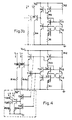
- the core of the cross-coupled current stabilizer means comprised of transistors T11, T12,T13 and T14, with resistors R11 and R12 is identical to the arrangement of that of Figure 3b.
- resistor R13 and transistor T17 are arranged identically to resistor R3 and transistor T7, as is transistor T16 relative to transistor T6.
- two additional transistors T19 and T20 are added to the circuit, and transistor T15 is arranged differently than transistor T5 of Figure 3b.
- transistor T19 is connected in parallel with cross-coupled transistor T11 and resistor R11 with the base of transistor T19 being connected to the base of cross-coupled transistor T11, and the emitter of transistor T19 being coupled to ground.
- the collector of transistor T19 is coupled to the base of transistor T15 (which is otherwise arranged as transistor T5 of Figure 3b), as well as to the emitter of cascode transistor T20.
- the base of transistor T20 is coupled to the base of transistor T14, and the collector of transistor T20 is coupled to the positive voltage rail Vcc. Loading the voltage output V out are a plurality of transistors with resistors coupling their emitters to the negative rail.
- a first set of transistors T18a and T18b with resistors R14a and R14b are shown as providing current outputs from the voltage output obtained at the junction of transistors T15 and T16.
- one or more additional blocks of multiple current source output circuitry can be provided such as by providing transistors T25 and T26 in parallel with transistors T15 and T16 and by providing transistors T28a, T28b... and resistors R24a, R24b... therewith.
- the current through transistor T16 likewise varies in the same manner as the current through transistor T12.
- the output voltage V out is equal to V be14 + (R13/R11) ⁇ (kT/q)ln(p) ⁇ , and represents the same stabilized voltage which is seen at the voltage output in Figure 3b.
- the output currents flowing through the various output transistors and resistors can be controlled as desired, but are still somewhat temperature dependent.
- the multiple current source arrangement of Figure 4 permits heavier loading on the output as transistors T19 and T20 decouple the loading of the multiple current sources from the stabilized cross-coupled circuit T11, T12, T13, T14.
- Transistor T17 operates as a current gain stage and supplies current to the base of the multiple output current sources (T16, T26%) and resistor R13. In this way, the operation of the basic stabilizer is not influenced by the output loading.
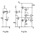
- FIG. 5a a temperature-independent, positive rail-independent current source is seen.
- the core cross-coupled current stabilizer circuit including cross-coupled transistors T31 and T32, and transistors T33 and T34 are provided with resistor R31 coupling the emitter of transistor T31 to ground.
- a resistor R32 is provided which couples the collector of transistor T33 with the positive rail, and cascoded transistors T35 and T36 are arranged with transistor T35 mirroring the current through transistor T32, and the voltage output being at the emitter of transistor T36.
- a transistor-diode T37 is provided with its emitter coupled to the collector-base of transistor T34, and its collector-base coupled to the base of transistor T36 as well as to resistor R32.
- an additional transistor T44 is provided with its collector coupled to a node between the output transistor T38 and its associated emitter resistor R34, its base coupled to the collector of transistor T32, and its emitter coupled to the negative rail.
- the base-emitter voltage of transistor T44 must be equal to the voltage drops across the base-emitter junction of transistor T31 and resistor R31.
- the collector current of transistor T44 is substantially equal to the collector currents of transistors T31 and T34 which have a positive temperature coefficient. Adding the currents through transistor T44 and the current through resistor R34 together results in an output current with an adjustable temperature coefficient.
- the value of resistor R34 can be chosen to be approximately equal to the bandgap voltage of silicon divided by the output current (V gap /I out ). By adjusting R31 properly, a desired output current is obtained.
- FIG. 5b shows an alternative manner of arranging the output circuitry of Figure 5a to create a temperature-independent current source.
- transistor T54a and T54b are provided in cascode relationship.
- Transistor T54a has its base coupled to the emitter of transistor T36 as well as to the base of transistor T38, its collector coupled to the collector of transistor T38 (i.e. to the current source output), and its emitter coupled to the collector-base of transistor T54b.
- the emitter of transistor T54b is coupled to the negative rail.
- the temperature coefficient of the current flowing through transistors T54a and T54b may be balanced with the temperature coefficient of the current flowing through transistor T38 and resistor R34 to provide the substantially temperature independent current source.
- a multiple current source which is independent of temperature may be obtained.
- a plurality of transistors can be connected with their bases coupled to the base of transistor T38 and their emitters coupled to resistors which are coupled to the negative rail.
- a plurality of transistors such as transistor T44 can be coupled to the base of transistors T31 and T44 with their collectors coupled to the emitters of their respectively associated output transistors and their emitters coupled to the negative rail.
- the current outputs can be made temperature independent by carefully choosing the values of their respective degeneration resistors. Of course, resistor R31 must likewise be chosen carefully.
- multiple current sources can be created with the output circuitry of Figure 5b.
- three additional transistors and one degeneration resistor are used and arranged in a similar manner to transistors T54a, T54b, and T38, and resistor R34 of Figure 5b.
- two additional transistors having coupled bases and coupled collectors would have their bases coupled to the base of transistor T38 (their collectors not being coupled to the collector thereof).
- An additional transistor arranged as a diode would couple the emitter of one transistor to the negative rail, while the degeneration resistor would couple the emitter of the other transistor to the negative rail.
Landscapes
- Engineering & Computer Science (AREA)
- Microelectronics & Electronic Packaging (AREA)
- Physics & Mathematics (AREA)
- Power Engineering (AREA)
- Nonlinear Science (AREA)
- Electromagnetism (AREA)
- General Physics & Mathematics (AREA)
- Radar, Positioning & Navigation (AREA)
- Automation & Control Theory (AREA)
- Control Of Electrical Variables (AREA)
- Amplifiers (AREA)
Claims (15)
- Strom-/Spannungsquelle zwischen einer positiven und einer negativen Spannungsversorgungsschiene, die folgendes umfaßt:
ein kreuzgekoppeltes Stromstabilisator-Mittel mit einem ersten (T1) und einem zweiten (T2) kreuzgekoppelten Bipolartransistor, die beide über einen Emitter verfügen, wobei die Emitterfläche des ersten Transistors (T1) größer ist als die Emitterfläche des zweiten Transistors (T2), mit einem vierten Transistor (T4), der als Diode geschaltet ist und dessen Basis mit der Basis eines dritten Bipolartransistors (T3) gekoppelt ist und dessen Kollektor mit der positiven Schiene gekoppelt ist, wobei der Emitter des zweiten Transistors (T2) mit der negativen Schiene gekoppelt ist,
einen ersten Widerstand (R1), der zwischen den Emitter des ersten Transistors (T1) und die negative Schiene geschaltet ist,
einen zweiten Widerstand (R2), der zwischen die positive Schiene und den Kollektor des dritten Transistors (T3) geschaltet ist,
einen fünften Transistor (T6), dessen Kollektor mit der positiven Schiene gekoppelt ist,
wobei alle fünf genannten Bipolartransistoren die gleiche Polarität aufweisen,
ein Stromspiegel-Mittel zur Spiegelung eines durch einen der genannten kreuzgekoppelten Transistoren fließenden Stroms, wobei der Emitter des fünften Transistors (T6) mit einem Ausgang des Stromspiegel-Mittels verbunden ist, dadurch gekennzeichnet, daß die Basis des fünften Transistors (T6) mit dem Kollektor des vierten Transistors (T4) verbunden ist, daß der in einem der genannten kreuzgekoppelten Transistoren fließende gespiegelte Strom der Kollektorstrom des zweiten Transistors (T2) ist, daß der Emitter des dritten Transistors (T3) mit dem Kollektor des genannten zweiten Transistors (T2) verbunden ist und daß der Emitter des vierten Transistors (T4) mit dem Kollektor des genannten ersten Transistors (T1) gekoppelt ist. - Strom-/Spannungsquelle nach Anspruch 1, wobei:
das genannte Stromspiegel-Mittel einen sechsten Bipolartransistor (T5) in Verbindung mit dem genannten zweiten kreuzgekoppelten Transistor (T2) enthält, wobei die Basis des sechsten Transistors (T5) mit der Basis des genannten zweiten kreuzgekoppelten Transistors (T2) verbunden ist, der Emitter mit dem Emitter des zweiten kreuzgekoppelten Transistors (T2) verbunden ist und der Kollektor mit dem genannten Emitter des fünften Transistors (T6) gekoppelt ist, wobei der Kollektor des genannten zweiten kreuzgekoppelten Transistors (T2) ein Eingang des genannten Stromspiegels ist. - Strom-/Spannungsquelle nach Anspruch 1 oder 2, die weiterhin enthält:
einen dritten Widerstand (R3), der die Basis und den Kollektor des genannten vierten Transistors (T4) mit der Basis des genannten fünften Bipolartransistors (T6) verbindet. - Strom-/Spannungsquelle nach Anspruch 3, die weiterhin enthält:
einen siebten Bipolartransistor (T7) der gleichen Polarität, dessen Emitter mit der Basis des genannten fünften Transistors (T6) verbunden ist, dessen Basis mit dem Kollektor des genannten dritten Transistors (T3) verbunden ist und dessen Kollektor mit der genannten positiven Schiene gekoppelt ist. - Strom-/Spannungsquelle nach Anspruch 3, wobei:
die Emitterflächen des dritten (T3), des vierten (T4) und des fünften (T6) Transistors im wesentlichen dem Emitter des genannten zweiten (T2) Transistors entsprechen. - Strom-/Spannungsquelle nach Anspruch 1, 2, 3, 4 oder 5, gekennzeichnet durch
mindestens einen achten bipolaren Ausgangstransistor (T8) der gleichen Polarität, wobei die Basis jedes achten Ausgangstransistors (T8) mit dem genannten Emitter des genannten fünften Transistors (T6) gekoppelt ist, der Kollektor jedes achten Ausgangstransistors (T8) einen hiermit verbundenen Knotenpunkt hat und als Stromquelle dient. - Strom-/Spannungsquelle nach Anspruch 6, die weiterhin enthält:
mindestens einen vierten Widerstand (R4), wobei jeder vierte Widerstand (R4) den Emitter eines der achten Ausgangstransistoren (T8) mit der genannten negativen Schiene verbindet. - Strom-/Spannungsquelle nach Anspruch 7, wobei:
mindestens ein achter Ausgangstransistor (T8) eine Vielzahl von Ausgangstransistoren enthält und mindestens ein vierter Widerstand (R4) eine entsprechende Vielzahl von vierten Widerständen (R4) umfaßt. - Strom-/Spannungsquelle nach Anspruch 7, die weiterhin enthält:
einen neunten Bipolartransistor (T20) der gleichen Polarität, dessen Basis mit der Basis des genannten vierten Transistors (T4, T14) verbunden ist, dessen Kollektor mit der positiven Schiene gekoppelt ist und dessen Emitter mit der Basis des genannten sechsten Transistors (T5, T15) verbunden ist, und
einen zehnten Bipolartransistor (T19) der gleichen Polarität, dessen Kollektor mit der genannten Basis des genannten sechsten Transistors (T5, T15) verbunden ist, dessen Basis mit der Basis des genannten ersten kreuzgekoppelten Transistors (T1, T11) verbunden ist und dessen Emitter mit der negativen Schiene gekoppelt ist. - Strom-/Spannungsquelle nach Anspruch 9, die weiterhin enthält:
eine oder mehrere Stufen, die mit dem Emitter des genannten neunten Transistors (T20) und dem Emitter des genannten siebten Transistors (T7, T17) verbunden sind, wobei jede Stufe mehrere Transistoren (T26, T25, T28) und mindestens einen Widerstand (R24) enthält, die auf gleiche Weise geschaltet sind wie eine Anordnung aus dem genannten fünften Transistor (T6), dem sechsten Transistors (T5), mindestens einem achten Transistor (T8) und mindestens einem vierten Widerstand (R4). - Strom-/Spannungsquelle nach Anspruch 7 oder 10, wobei:
die genannten achten Ausgangstransistoren (T8) und die genannten vierten Widerstände (R4) für jedes Transistor-Widerstand-Paar so gewählt werden, daß ein Kennwert der Emitterfläche des genannten achten Ausgangstransistors (T8) multipliziert mit dem Widerstandswert des genannten vierten Widerstandes (R4) einen im wesentlichen identischen Wert für jedes genannte Paar ergibt, um im wesentlichen gleiche Ausgangsströme zu erhalten. - Strom-/Spannungsquelle nach Anspruch 7 oder 10, wobei:
die genannten achten Ausgangstransistoren (T8) und die genannten vierten Widerstände (R4) für jedes Transistor-Widerstand-Paar so gewählt werden, daß ein Kennwert der Emitterfläche des genannten achten Ausgangstransistors (T8) multipliziert mit dem Widerstandswert des genannten vierten Widerstandes (R4) einen Wert ergibt, der eine binäre Potenz eines anderen Transistor-Widerstand-Paares ist, um im wesentlichen binär gewichtete Ausgangsströme zu erhalten. - Strom-/Spannungsquelle nach Anspruch 6, die weiterhin enthält:
einen elften Bipolartransistor (T37) der gleichen Polarität, der als Diode geschaltet ist und dessen Emitter und Kollektor mit dem Kollektor des genannten vierten Transistors (T34) bzw. mit der Basis des fünften Transistors (T36) gekoppelt ist,
mindestens einen zwölften Bipolartransistor (T44) der gleichen Polarität für jeden achten Transistor (T38), wobei die Basis des zwölften Transistors (T44) mit dem Kollektor des genannten ersten kreuzgekoppelten Transistors (T31) verbunden ist, der Kollektor mit dem Emitter des entsprechenden achten Ausgangstransistors (T38) gekopppelt ist und der Emitter mit der genannten negativen Schiene verbunden ist. - Strom-/Spannungsquelle nach Anspruch 13, wobei:
mindestens ein vierter Widerstand (R4) so gewählt wird, daß sein Widerstandswert im wesentlichen der Bandlücken-Spannung des Siliziums geteilt durch einen zu dem Kollektor des jeweiligen achten Transistors (T8) fließenden Ausgangsstrom entspricht. - Strom-/Spannungsquelle nach Anspruch 13, wobei:
mindestens ein zwölfter Transistor (T44) durch mindestens einen dreizehnten Bipolartransistor (T54b) der gleichen Polalität für jeden der genannten achten Transistoren (T38) ersetzt wird, wobei die Basis und der Kollektor des dreizehnten Transistors mit dem Emitter des genannten achten Transistors verbunden ist und sein Emitter mit der negativen Schiene gekoppelt ist.
Applications Claiming Priority (2)
| Application Number | Priority Date | Filing Date | Title |
|---|---|---|---|
| US156381 | 1988-02-16 | ||
| US07/156,381 US4816742A (en) | 1988-02-16 | 1988-02-16 | Stabilized current and voltage reference sources |
Publications (2)
| Publication Number | Publication Date |
|---|---|
| EP0329232A1 EP0329232A1 (de) | 1989-08-23 |
| EP0329232B1 true EP0329232B1 (de) | 1993-10-20 |
Family
ID=22559338
Family Applications (1)
| Application Number | Title | Priority Date | Filing Date |
|---|---|---|---|
| EP89200309A Expired - Lifetime EP0329232B1 (de) | 1988-02-16 | 1989-02-10 | Stabilisierte Strom- und Spannungsquellen |
Country Status (6)
| Country | Link |
|---|---|
| US (1) | US4816742A (de) |
| EP (1) | EP0329232B1 (de) |
| JP (1) | JP2752683B2 (de) |
| KR (1) | KR0136874B1 (de) |
| DE (1) | DE68909966T2 (de) |
| HK (1) | HK163895A (de) |
Families Citing this family (17)
| Publication number | Priority date | Publication date | Assignee | Title |
|---|---|---|---|---|
| US5015942A (en) * | 1990-06-07 | 1991-05-14 | Cherry Semiconductor Corporation | Positive temperature coefficient current source with low power dissipation |
| US5049807A (en) * | 1991-01-03 | 1991-09-17 | Bell Communications Research, Inc. | All-NPN-transistor voltage regulator |
| IT1245688B (it) * | 1991-04-24 | 1994-10-13 | Sgs Thomson Microelectronics | Struttura di compensazione in temperatura della corrente inversa di saturazione in transistori bipolari |
| FR2718259A1 (fr) * | 1994-03-30 | 1995-10-06 | Philips Composants | Circuit régulateur fournissant une tension indépendante de l'alimentation et de la température. |
| DE69511043T2 (de) * | 1994-04-08 | 2000-02-17 | Koninklijke Philips Electronics N.V., Eindhoven | Referenzspannungsquelle zur polarisierung von mehreren stromquelletransistoren mit temperaturkompensierter stromversorgung |
| US5453679A (en) * | 1994-05-12 | 1995-09-26 | National Semiconductor Corporation | Bandgap voltage and current generator circuit for generating constant reference voltage independent of supply voltage, temperature and semiconductor processing |
| US5760639A (en) * | 1996-03-04 | 1998-06-02 | Motorola, Inc. | Voltage and current reference circuit with a low temperature coefficient |
| US5686823A (en) * | 1996-08-07 | 1997-11-11 | National Semiconductor Corporation | Bandgap voltage reference circuit |
| JP3266177B2 (ja) * | 1996-09-04 | 2002-03-18 | 住友電気工業株式会社 | 電流ミラー回路とそれを用いた基準電圧発生回路及び発光素子駆動回路 |
| US6002293A (en) * | 1998-03-24 | 1999-12-14 | Analog Devices, Inc. | High transconductance voltage reference cell |
| KR100529557B1 (ko) * | 1998-04-10 | 2006-02-17 | 삼성전자주식회사 | 스텝다운 직류/직류 변환기 |
| US6144250A (en) * | 1999-01-27 | 2000-11-07 | Linear Technology Corporation | Error amplifier reference circuit |
| US6285244B1 (en) * | 1999-10-02 | 2001-09-04 | Texas Instruments Incorporated | Low voltage, VCC incentive, low temperature co-efficient, stable cross-coupled bandgap circuit |
| GB2355552A (en) | 1999-10-20 | 2001-04-25 | Ericsson Telefon Ab L M | Electronic circuit for supplying a reference current |
| DE10011669A1 (de) * | 2000-03-10 | 2001-09-20 | Infineon Technologies Ag | Schaltungsanordnung zum Erzeugen einer Gleichspannung |
| FR2821442A1 (fr) * | 2001-02-26 | 2002-08-30 | St Microelectronics Sa | Source de courant a faible tension d'alimentation et dont le courant varie en sens inverse de celui de la tension d'alimentation |
| US6570438B2 (en) * | 2001-10-12 | 2003-05-27 | Maxim Integrated Products, Inc. | Proportional to absolute temperature references with reduced input sensitivity |
Family Cites Families (7)
| Publication number | Priority date | Publication date | Assignee | Title |
|---|---|---|---|---|
| US3887863A (en) * | 1973-11-28 | 1975-06-03 | Analog Devices Inc | Solid-state regulated voltage supply |
| US3930172A (en) * | 1974-11-06 | 1975-12-30 | Nat Semiconductor Corp | Input supply independent circuit |
| US4177417A (en) * | 1978-03-02 | 1979-12-04 | Motorola, Inc. | Reference circuit for providing a plurality of regulated currents having desired temperature characteristics |
| DE2850826A1 (de) * | 1978-11-23 | 1980-06-04 | Siemens Ag | Referenzspannungsquelle, insbesondere fuer verstaerkerschaltungen |
| US4460865A (en) * | 1981-02-20 | 1984-07-17 | Motorola, Inc. | Variable temperature coefficient level shifting circuit and method |
| US4491780A (en) * | 1983-08-15 | 1985-01-01 | Motorola, Inc. | Temperature compensated voltage reference circuit |
| NL8501882A (nl) * | 1985-07-01 | 1987-02-02 | Philips Nv | Signaalspanning-stroom omzetter. |
-
1988
- 1988-02-16 US US07/156,381 patent/US4816742A/en not_active Expired - Lifetime
-
1989
- 1989-02-10 EP EP89200309A patent/EP0329232B1/de not_active Expired - Lifetime
- 1989-02-10 DE DE89200309T patent/DE68909966T2/de not_active Expired - Fee Related
- 1989-02-13 KR KR1019890001616A patent/KR0136874B1/ko not_active Expired - Fee Related
- 1989-02-14 JP JP1034865A patent/JP2752683B2/ja not_active Expired - Lifetime
-
1995
- 1995-10-19 HK HK163895A patent/HK163895A/en not_active IP Right Cessation
Also Published As
| Publication number | Publication date |
|---|---|
| KR890013861A (ko) | 1989-09-26 |
| JPH01245320A (ja) | 1989-09-29 |
| DE68909966T2 (de) | 1994-04-14 |
| EP0329232A1 (de) | 1989-08-23 |
| KR0136874B1 (ko) | 1998-05-15 |
| JP2752683B2 (ja) | 1998-05-18 |
| US4816742A (en) | 1989-03-28 |
| HK163895A (en) | 1995-10-27 |
| DE68909966D1 (de) | 1993-11-25 |
Similar Documents
| Publication | Publication Date | Title |
|---|---|---|
| EP0329232B1 (de) | Stabilisierte Strom- und Spannungsquellen | |
| US5982201A (en) | Low voltage current mirror and CTAT current source and method | |
| US6407622B1 (en) | Low-voltage bandgap reference circuit | |
| US4399399A (en) | Precision current source | |
| US5432432A (en) | Reference voltage generating circuit with temperature stability for use in CMOS integrated circuits | |
| US4308496A (en) | Reference current source circuit | |
| JP3039611B2 (ja) | カレントミラー回路 | |
| US6294902B1 (en) | Bandgap reference having power supply ripple rejection | |
| JPH0656571B2 (ja) | 温度補償付電圧基準回路 | |
| US4897595A (en) | Band-gap reference voltage circuit with feedback to reduce common mode voltage | |
| JPH11288321A (ja) | Npnデバイスを用いないcmos処理工程に対する正確なバンドギャップ回路 | |
| US4672304A (en) | Reference voltage source | |
| US5334929A (en) | Circuit for providing a current proportional to absolute temperature | |
| US4677368A (en) | Precision thermal current source | |
| EP0124918B1 (de) | Stromquellenanordnung | |
| US5528128A (en) | Reference voltage source for biassing a plurality of current source transistors with temperature-compensated current supply | |
| JP3334707B2 (ja) | チャージポンプ回路 | |
| EP0929021A1 (de) | Stromversorgungs- und Vorspannungsschaltung | |
| JPS6398159A (ja) | 温度補償された電流源およびこれを用いた電圧調整器 | |
| US4389619A (en) | Adjustable-gain current amplifier for temperature-independent trimming | |
| US5498952A (en) | Precise current generator | |
| JPH0624298B2 (ja) | 電流増幅回路 | |
| JP2002525738A (ja) | 電圧及び/又は電流基準回路 | |
| JP4130856B2 (ja) | 電流源回路 | |
| JPH0316646B2 (de) |
Legal Events
| Date | Code | Title | Description |
|---|---|---|---|
| PUAI | Public reference made under article 153(3) epc to a published international application that has entered the european phase |
Free format text: ORIGINAL CODE: 0009012 |
|
| AK | Designated contracting states |
Kind code of ref document: A1 Designated state(s): DE FR GB IT NL |
|
| 17P | Request for examination filed |
Effective date: 19900222 |
|
| 17Q | First examination report despatched |
Effective date: 19920630 |
|
| GRAA | (expected) grant |
Free format text: ORIGINAL CODE: 0009210 |
|
| AK | Designated contracting states |
Kind code of ref document: B1 Designated state(s): DE FR GB IT NL |
|
| PG25 | Lapsed in a contracting state [announced via postgrant information from national office to epo] |
Ref country code: NL Effective date: 19931020 |
|
| REF | Corresponds to: |
Ref document number: 68909966 Country of ref document: DE Date of ref document: 19931125 |
|
| ITF | It: translation for a ep patent filed | ||
| ET | Fr: translation filed | ||
| ITTA | It: last paid annual fee | ||
| NLV1 | Nl: lapsed or annulled due to failure to fulfill the requirements of art. 29p and 29m of the patents act | ||
| PLBE | No opposition filed within time limit |
Free format text: ORIGINAL CODE: 0009261 |
|
| STAA | Information on the status of an ep patent application or granted ep patent |
Free format text: STATUS: NO OPPOSITION FILED WITHIN TIME LIMIT |
|
| 26N | No opposition filed | ||
| ITPR | It: changes in ownership of a european patent |
Owner name: CAMBIO RAGIONE SOCIALE;PHILIPS ELECTRONICS N.V. |
|
| REG | Reference to a national code |
Ref country code: FR Ref legal event code: CD |
|
| REG | Reference to a national code |
Ref country code: FR Ref legal event code: CD |
|
| PGFP | Annual fee paid to national office [announced via postgrant information from national office to epo] |
Ref country code: FR Payment date: 20000222 Year of fee payment: 12 |
|
| PGFP | Annual fee paid to national office [announced via postgrant information from national office to epo] |
Ref country code: GB Payment date: 20000228 Year of fee payment: 12 |
|
| PGFP | Annual fee paid to national office [announced via postgrant information from national office to epo] |
Ref country code: DE Payment date: 20000419 Year of fee payment: 12 |
|
| PG25 | Lapsed in a contracting state [announced via postgrant information from national office to epo] |
Ref country code: GB Free format text: LAPSE BECAUSE OF NON-PAYMENT OF DUE FEES Effective date: 20010210 |
|
| GBPC | Gb: european patent ceased through non-payment of renewal fee |
Effective date: 20010210 |
|
| PG25 | Lapsed in a contracting state [announced via postgrant information from national office to epo] |
Ref country code: FR Free format text: LAPSE BECAUSE OF NON-PAYMENT OF DUE FEES Effective date: 20011031 |
|
| REG | Reference to a national code |
Ref country code: FR Ref legal event code: ST |
|
| PG25 | Lapsed in a contracting state [announced via postgrant information from national office to epo] |
Ref country code: DE Free format text: LAPSE BECAUSE OF NON-PAYMENT OF DUE FEES Effective date: 20011201 |
|
| PG25 | Lapsed in a contracting state [announced via postgrant information from national office to epo] |
Ref country code: IT Free format text: LAPSE BECAUSE OF NON-PAYMENT OF DUE FEES Effective date: 20050210 |