EP0329545A1 - Vorrichtung zur Berechnung von Paritätsbits einer Summe von zwei Zahlen - Google Patents
Vorrichtung zur Berechnung von Paritätsbits einer Summe von zwei Zahlen Download PDFInfo
- Publication number
- EP0329545A1 EP0329545A1 EP89400406A EP89400406A EP0329545A1 EP 0329545 A1 EP0329545 A1 EP 0329545A1 EP 89400406 A EP89400406 A EP 89400406A EP 89400406 A EP89400406 A EP 89400406A EP 0329545 A1 EP0329545 A1 EP 0329545A1
- Authority
- EP
- European Patent Office
- Prior art keywords
- bits
- operator
- group
- outputs
- numbers
- Prior art date
- Legal status (The legal status is an assumption and is not a legal conclusion. Google has not performed a legal analysis and makes no representation as to the accuracy of the status listed.)
- Granted
Links
Images



Classifications
-
- G—PHYSICS
- G06—COMPUTING OR CALCULATING; COUNTING
- G06F—ELECTRIC DIGITAL DATA PROCESSING
- G06F11/00—Error detection; Error correction; Monitoring
- G06F11/07—Responding to the occurrence of a fault, e.g. fault tolerance
- G06F11/08—Error detection or correction by redundancy in data representation, e.g. by using checking codes
- G06F11/10—Adding special bits or symbols to the coded information, e.g. parity check, casting out 9's or 11's
-
- G—PHYSICS
- G06—COMPUTING OR CALCULATING; COUNTING
- G06F—ELECTRIC DIGITAL DATA PROCESSING
- G06F7/00—Methods or arrangements for processing data by operating upon the order or content of the data handled
- G06F7/38—Methods or arrangements for performing computations using exclusively denominational number representation, e.g. using binary, ternary, decimal representation
- G06F7/48—Methods or arrangements for performing computations using exclusively denominational number representation, e.g. using binary, ternary, decimal representation using non-contact-making devices, e.g. tube, solid state device; using unspecified devices
- G06F7/50—Adding; Subtracting
Definitions
- the invention lies in the field of adders used in particular in computer processors.
- the invention relates more particularly to circuits used to calculate the parity bits associated with the binary number which is the result of an addition calculated by an adder receiving as input two binary numbers.
- parity bits associated with words or binary numbers are used to be able to detect whether these words or these numbers have not been affected by errors after having been manipulated in the processing circuits.
- the parity bit of a group of bits is usually defined as the result of the combination by "EXCLUSIVE OR" operations relating to the set of bits constituting the group.
- the parity bit therefore takes the value “1” if the number of "1" contained in the group is odd.
- the parity bit takes the value complementary to the value it should have. Errors can therefore be detected by simple comparison between the actual parity calculated from the group and the expected parity corresponding to the value of the parity bit.
- the words can be formed from several groups of bits and to each group there is associated a parity bit. A word can therefore be associated with several parity bits.
- the result of this operation should also be associated with one or more parity bits. This is particularly the case for addition operations.
- the parity bit or bits of the result of an addition could be calculated directly from the result.
- the parity bits of the result can only be obtained long after the result itself, which delays the moment when the result and its associated parity bits can be used in the subsequent processing.
- the parity bits can be calculated independently of the result itself since there is then a check on the accuracy of the addition.
- the object of the invention is to allow the parity bits of the sum of two numbers to be calculated in the shortest possible time.
- the advantage of a rapid calculation of the parity bits lies in the fact that this calculation does not delay the moment when the adder becomes available again for the following operation. As a result, the computing unit will be able to work at a higher frequency.
- this word When the numbers to be added include a large number of bits, it is more advantageous to consider this word as the concatenation of several groups of bits and to associate with each of these groups a parity bit. For example, a 64-bit word can be associated with eight parity bits, each parity bit being associated with a group of eight bits of the word. This method makes it possible in particular to improve the detection of errors, in particular in the case of multiple errors relating to different groups.
- the parity bit associated with a group extracted from the carry word depends in principle on all the carry bits formed during the addition.
- the invention relates to a solution for calculating the parity bits associated with the groups forming the carry word according to which once the computation of the carry bits performed, the time then necessary to calculate the parity bits is reduced to the maximum.
- This result is made possible by the fact that the device according to the invention performs this calculation in two stages: - a first step which uses as input variables variables which depend only on the numbers to be added; - a second quick step involving carry bits.
- the first step takes place during the calculation of the deductions by the anticipation circuit of the adder and, taking into account the relative slowness of this calculation, this first step is designed so as to perform the maximum of preparatory calculations, thus allowing to simplify the second step, therefore made faster.
- the subject of the invention is a device for calculating the parity bit associated with at least one group of m consecutive bits extracted from the carry word appearing during the addition of two binary numbers, said numbers each comprising at least one group of m bits, said groups belonging respectively to said numbers and to the carry word being made up of bits of the same weight respectively, said groups extracted from said numbers being formed respectively of bits a m , ..., a i , ..., a2 , a1 and bits b m , ..., b i .
- the index i indicating the weight in the group of the associated bit
- the previous device can then be modified so as to involve parity bits from each of the operands to directly supply the parity bits associated with their sum, without thereby delaying the calculation.
- the invention therefore also relates to a device for calculating the parity bit associated with at least one group of m bits extracted from the sum of two numbers, characterized in that it comprises a device for calculating according to the preceding device but to which are added additional circuits "OR EXCLUSIVE" to introduce the PA and PB parities of said numbers and arranged so as to: either replace any of the outputs G i of the first operator with the result of the operation PA ⁇ PB ⁇ G i carried out by said additional circuits, - Either replace any two outputs G i and G j of the first operator by, respectively, the result of the operations PA ⁇ G i and PB ⁇ G j .
- a and B of N bits consisting respectively of the bits a N , a N - 1 , ..., a i , ..., a2, a1 and b N , b N - 1 , ... , b i , ..., b2, b1
- a common method for performing the sum of these two numbers consists in using a circuit for anticipation of the carry word C formed of the carry bits c i involved in the addition.
- the carry bits can be calculated step by step from the variables p i , g i which depend on the only bits a i , b i of the operands. This calculation is carried out by the anticipation of deductions circuit mentioned above.
- the operands A and B, the carry word C and the sum S are for example constituted respectively by the groups A1, A2, A3, A4, groups B1, B2, B3, B4, groups C1, C2, C3, C4 and groups S1, S2, S3, S4.
- Each group, for example A j associates a corresponding parity bit, for example PA j .
- the parity bits we will only consider the homologous groups of the operands, the carry word and the sum, that is to say the groups made up of the bits of the same weight. .
- the indices identifying the groups will no longer be used.
- the index i of a bit will be the weight relative to the group considered and will therefore have a value between 1 and m, the weight 1 being the lowest weight in the group.
- FIG. 1 represents an adder associated with a parity bit generator according to the invention.
- a and B are made up of four groups of bits, respectively A1, A2, A3, A4 and B1, B2, B3, B4.
- Each group is associated with a corresponding parity bit.
- group A1 is associated with the parity bit PA1
- group A2 is associated with the parity bit PA2, etc.
- the operands A and B as well as the parity bits associated with these two operands are contained in respective registers RA, RB, RPA and RPB.
- the group A1 consists of m bits a 1i and the group B1 consists of m bits b 1i .
- circuits 12, 13 and 14 associated with the other groups are identical to the circuit 11, all of these circuits forming the first stage 10 of the adder.
- a anticipation circuit for reservoirs 20a receives the outputs of the first stage 10 as an input.
- the circuit 20a known per se makes it possible to calculate all the retained c 1i , c 2i , c 3i , and c 4i involved in the addition of the two operands.
- This circuit 20a can be considered as consisting of several circuits 21a, 22a, 23a and 24a respectively associated with the groups from which the operands are formed.
- a last stage 30 made up of "EXCLUSIVE OR" receives the deductions from the circuit 20a and the variables p 1i to p 4i from the first stage 10.
- the circuit 30 outputs the bits s 1i to s 4i of the result S of the addition .
- the circuit 30 can also be considered as consisting of the circuits 31, 32, 33 and 34 respectively associated with the groups forming the operands.
- the parity generator comprises a set made up of four operators 41, 42, 43 and 44 receiving respectively the parity bits of the homologous groups of the operands and the variables coming from the first stage 10.
- the operator 41 associated with the first group receives the parities PA1, PB1 and the variables p 1i and g 1i from the circuit 11. As a function of these signals, the operator 41 delivers the two variables X1 and Y1 verifying the equations which have been exposed previously but in the absence of evidence.
- circuits 42, 43, 44 respectively deliver the variables X2, Y2; X3, Y3; X4, Y4.
- PS1 to PS4 thus obtained are therefore the parity bits associated with each of the groups extracted from the sum.
- stages 10 and 30 of the adder consist of conventional logic circuits of the "AND” and "OR EXCLUSIVE" type. Their realization is within the reach of those skilled in the art and will therefore not be described in detail.
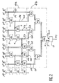
- FIG. 2 represents a circuit allowing the calculation of the parity bit associated with the carry bits of a group of eight bits.
- the circuit of FIG. 2 comprises a first operator 41a receiving the variables p1, g1 to p7, g7 calculated by the circuit 11 exposed previously or by a separate but identical circuit.
- This circuit 11 can indeed be common with the adder but if one wishes to improve the integrity of the circuit, it is preferable to use a circuit 11 independent of the adder because the use of a common circuit 11 would mask errors that could occur in this circuit.
- the relation which links the pair of output variables P z , G z to the two pairs of input variables P x , G x and P y , G y has the important property of being associative. Thanks to this property, it is possible to arrange the modules M1 so as to calculate the variables P i and G i while minimizing the number of layers of this circuit, that is to say the number of these modules put Cascade.
- the initial assembly for i between 1 and 2 n being carried out, the assembly for i between 2 n + 1 and 2 n + 1 is obtained by adding M1 modules arranged according to this initial assembly but shifted by 2 n rows towards the weights strong, thus providing new outputs. There are then 2 n additional modules M1 which combine the most significant outputs P2n, G2n from the initial assembly and, respectively, each of these new outputs.
- the outputs P i , G i of the operator 41a are then applied to the inputs of the second operator 41b.
- the number of layers necessary to obtain the variables P i , G i is equal to n.
- the number of circuit layers necessary to obtain X and Y is equal to 2n and consequently the total number of layers to obtain the parity PC is equal to 2n + 1.
- the parity generator is consisting of a seven-layer circuit.
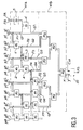
- the preceding circuit must be modified so as to involve the parity bits associated with the groups extracted from the operands.
- FIG 3 shows an example of modification of the diagram in Figure 2 to obtain this result.
- the operator output 51 now represents the parity bit PS of the sum for the group considered.
- FIG. 4 represents a parity of an embodiment of an adder comprising the anticipation circuit 20a of the carry bits. Although this circuit in itself is not the object of the present invention, its description is useful because it will allow a better understanding of the context of the invention.
- the anticipation circuit for the holding bits of the first group 21a receives the variable c in and the outputs of the first stage 10 as input.
- the adder can be used to perform subtraction. Indeed, the subtraction operation A - B amounts to calculating A + B * + 1, B * being the complement of B.
- This circuit includes a plurality of modules M1 defined above and intended to calculate the variables P i and G i .
- the modules of type M1 and M3 are arranged in an arrangement called "recurrence solver" known in the art of adders.
- This circuit provides as an output the reservoirs c i which are then combined in circuit 31 with the variables p i of the same weight.
- the circuit 31 delivers the bits s i of the result of the addition.
- the adder also includes circuits 22a and 32 for the second group and other circuits not shown for the following groups.
- Such a circuit could be identical to that used in the adder, but it is advantageous to simplify it so that it provides only the carry bits involved in the generation of the parity bits.
- FIG. 5 represents such a circuit for anticipating specific holdbacks of the parity generator.
- This circuit represents the case where the groups to which the parities relate comprise eight bits.
- a first sub-assembly 21 provides the carry c9 which will serve as an input signal to circuit 52 of the second group.
- Circuit 22 provides the retainer c17 serving as input to circuit 53 of the third group.
- the circuit 23 not shown will provide the carry csistede for the fourth group.
- the anticipation circuit of the deductions will include r layers.
- the adder will have a total of r + 1 layers. This result should be compared to the 2n + 1 layers necessary to make the parity generator. It will therefore be necessary to choose n as a function of r.
- FIG. 6 represents a CMOS circuit making it possible to obtain the variable G z * which is the complement of G z .
- This circuit can then be associated with a NAND gate (NAND) providing P z * which is the complement of P z .
- FIG. 7 presents a circuit making it possible to obtain the dual function of the previous one.
- G x *, G y *, P y * being respectively the complements of G x , G y , P y
- circuit of figure 7 could be associated with an NI (NOR) gate. Consequently, the circuits of FIGS. 2 and 3 can be produced using instead of the modules M1 defined above, alternately these circuits without changing the final result, provided that inverters are provided at the appropriate inputs.
- NI NOR
- circuits can also be used to make the modules M3 of the anticipation circuit of the reservoirs.
- FIG. 8 shows by way of illustration an example of a CMOS circuit for performing the "EXCLUSIVE OR" function. This circuit could be used for example to produce the modules M2 and 51 of FIGS. 2 and 3.
Landscapes
- Engineering & Computer Science (AREA)
- Theoretical Computer Science (AREA)
- Quality & Reliability (AREA)
- Physics & Mathematics (AREA)
- General Engineering & Computer Science (AREA)
- General Physics & Mathematics (AREA)
- Error Detection And Correction (AREA)
- Detection And Correction Of Errors (AREA)
Applications Claiming Priority (2)
| Application Number | Priority Date | Filing Date | Title |
|---|---|---|---|
| FR8801910A FR2627605B1 (fr) | 1988-02-18 | 1988-02-18 | Dispositif pour le calcul des bits de parite d'une somme de deux nombres |
| FR8801910 | 1988-02-18 |
Publications (2)
| Publication Number | Publication Date |
|---|---|
| EP0329545A1 true EP0329545A1 (de) | 1989-08-23 |
| EP0329545B1 EP0329545B1 (de) | 1991-11-21 |
Family
ID=9363358
Family Applications (1)
| Application Number | Title | Priority Date | Filing Date |
|---|---|---|---|
| EP89400406A Expired - Lifetime EP0329545B1 (de) | 1988-02-18 | 1989-02-14 | Vorrichtung zur Berechnung von Paritätsbits einer Summe von zwei Zahlen |
Country Status (5)
| Country | Link |
|---|---|
| US (1) | US4958353A (de) |
| EP (1) | EP0329545B1 (de) |
| JP (1) | JP2608600B2 (de) |
| DE (1) | DE68900439D1 (de) |
| FR (1) | FR2627605B1 (de) |
Cited By (1)
| Publication number | Priority date | Publication date | Assignee | Title |
|---|---|---|---|---|
| EP0655685A1 (de) | 1993-11-30 | 1995-05-31 | Bull S.A. | Einrichtung zum Berechnen von Paritätsbits in Verbindung mit einer Summe zweier Zahlen |
Families Citing this family (2)
| Publication number | Priority date | Publication date | Assignee | Title |
|---|---|---|---|---|
| GR920100163A (el) * | 1992-04-21 | 1993-12-30 | Koloni Sofia & Sia E E | Τεχνικές κατασκευές αυτοεπαλη?ευομένων μονάδων εκτέλεσης αρι?μητικών πράξεων & μονάδων επεξεργασίας δεδομένων βασιζόμενες σε κώδικες διπλής γραμμής & κώδικες άρτιας ή περιττής ισοτιμίας. |
| US5966029A (en) * | 1997-07-15 | 1999-10-12 | Motorola, Inc. | Multi-bit exclusive or |
Citations (2)
| Publication number | Priority date | Publication date | Assignee | Title |
|---|---|---|---|---|
| US4224680A (en) * | 1978-06-05 | 1980-09-23 | Fujitsu Limited | Parity prediction circuit for adder/counter |
| EP0193711A1 (de) * | 1985-01-25 | 1986-09-10 | Siemens Aktiengesellschaft | Schaltungsanordnung zur Funktionsüberwachung eines arithmetische Operationen ausführenden Rechenwerkes anhand von Paritätsbits |
Family Cites Families (2)
| Publication number | Priority date | Publication date | Assignee | Title |
|---|---|---|---|---|
| US3925647A (en) * | 1974-09-30 | 1975-12-09 | Honeywell Inf Systems | Parity predicting and checking logic for carry look-ahead binary adder |
| JPS5613336A (en) * | 1979-07-14 | 1981-02-09 | Towa Seiko Kk | Hand labeler |
-
1988
- 1988-02-18 FR FR8801910A patent/FR2627605B1/fr not_active Expired - Lifetime
-
1989
- 1989-02-14 DE DE8989400406T patent/DE68900439D1/de not_active Expired - Lifetime
- 1989-02-14 EP EP89400406A patent/EP0329545B1/de not_active Expired - Lifetime
- 1989-02-17 US US07/311,736 patent/US4958353A/en not_active Expired - Lifetime
- 1989-02-17 JP JP1038109A patent/JP2608600B2/ja not_active Expired - Fee Related
Patent Citations (2)
| Publication number | Priority date | Publication date | Assignee | Title |
|---|---|---|---|---|
| US4224680A (en) * | 1978-06-05 | 1980-09-23 | Fujitsu Limited | Parity prediction circuit for adder/counter |
| EP0193711A1 (de) * | 1985-01-25 | 1986-09-10 | Siemens Aktiengesellschaft | Schaltungsanordnung zur Funktionsüberwachung eines arithmetische Operationen ausführenden Rechenwerkes anhand von Paritätsbits |
Non-Patent Citations (1)
| Title |
|---|
| IBM TECHNICAL DISCLOSURE BULLETIN, vol. 23, no. 12, mai 1981, pages 5498-5502, IBM Corp., New York, US; P. KALANDRA et al.: "Parity predict of a sum" * |
Cited By (3)
| Publication number | Priority date | Publication date | Assignee | Title |
|---|---|---|---|---|
| EP0655685A1 (de) | 1993-11-30 | 1995-05-31 | Bull S.A. | Einrichtung zum Berechnen von Paritätsbits in Verbindung mit einer Summe zweier Zahlen |
| FR2713364A1 (fr) * | 1993-11-30 | 1995-06-09 | Bull Sa | Dispositif de calcul des bits de parité associés à une somme de deux nombres. |
| US5689451A (en) * | 1993-11-30 | 1997-11-18 | Bull S.A. | Device for calculating parity bits associated with a sum of two numbers |
Also Published As
| Publication number | Publication date |
|---|---|
| JP2608600B2 (ja) | 1997-05-07 |
| US4958353A (en) | 1990-09-18 |
| FR2627605B1 (fr) | 1990-06-15 |
| DE68900439D1 (de) | 1992-01-02 |
| FR2627605A1 (fr) | 1989-08-25 |
| EP0329545B1 (de) | 1991-11-21 |
| JPH01245334A (ja) | 1989-09-29 |
Similar Documents
| Publication | Publication Date | Title |
|---|---|---|
| Parhami | Carry-free addition of recoded binary signed-digit numbers | |
| JP2536452B2 (ja) | 光電子記憶処理装置および光学式修正符号付きディジット算術演算実行方法 | |
| EP0333599B1 (de) | Parametrischer Galois-Körper-Multiplizierer-Addierer und dessen Benutzung in einem digitalen Signalprozessor | |
| FR2605769A1 (fr) | Operateur polynomial dans les corps de galois et processeur de traitement de signal numerique comportant un tel operateur | |
| EP0692762B1 (de) | Logikschaltung zur parallelen Multiplikation | |
| FR2819073A1 (fr) | Microarchitecture d'unite arithmetique | |
| EP3503103A1 (de) | System, das einen adaptierten speicher zur durchführung von rechenoperationen umfasst | |
| FR2593620A1 (fr) | Circuit arithmetique et logique multifonction | |
| EP0110767B1 (de) | Schneller binärer Multiplizierer | |
| EP0262032B1 (de) | Binärer Addierer mit festem Operand und paralleler/serieller Multiplikator mit solchen Addierern | |
| EP0018298A1 (de) | Verfahren zum Ermitteln eines numerischen Rechenergebnisses in Gleitkommadarstellung mit der Anzahl der richtigen signifikativen Ziffern und numerische Recheneinrichtung zur Durchführung dieses Verfahrens | |
| EP0437876A1 (de) | Programmierbarer serieller Multiplikator | |
| EP0329545B1 (de) | Vorrichtung zur Berechnung von Paritätsbits einer Summe von zwei Zahlen | |
| FR2624282A1 (fr) | Comparateur binaire et operateur de tri de nombres binaires | |
| US20040186872A1 (en) | Transitive processing unit for performing complex operations | |
| EP0476592A2 (de) | Adressengenerator für den Datenspeicher eines Prozessors | |
| EP0309348B1 (de) | Binäre Additions- und Multiplikationsvorrichtung | |
| EP0655685B1 (de) | Einrichtung zum Berechnen von Paritätsbits in Verbindung mit einer Summe zweier Zahlen | |
| EP0341097B1 (de) | Rekursiver Addierer zur Berechnung der Summe zweier Operanden | |
| EP0239168B1 (de) | Arithmetisch-logische Schaltung | |
| EP0375054B1 (de) | Künstliche neuronale integrierte Schaltung mit Lernmitteln | |
| KR100241071B1 (ko) | 합과 합+1을 병렬로 생성하는 가산기 | |
| SU726527A1 (ru) | Устройство дл сравнени чисел | |
| JPS62118436A (ja) | 加算器 | |
| FR2538579A1 (fr) | Operateur elementaire, notamment pour multiplieur du type en cascade |
Legal Events
| Date | Code | Title | Description |
|---|---|---|---|
| PUAI | Public reference made under article 153(3) epc to a published international application that has entered the european phase |
Free format text: ORIGINAL CODE: 0009012 |
|
| 17P | Request for examination filed |
Effective date: 19890607 |
|
| AK | Designated contracting states |
Kind code of ref document: A1 Designated state(s): DE FR GB NL |
|
| 17Q | First examination report despatched |
Effective date: 19910130 |
|
| GRAA | (expected) grant |
Free format text: ORIGINAL CODE: 0009210 |
|
| AK | Designated contracting states |
Kind code of ref document: B1 Designated state(s): DE FR GB NL |
|
| GBT | Gb: translation of ep patent filed (gb section 77(6)(a)/1977) | ||
| REF | Corresponds to: |
Ref document number: 68900439 Country of ref document: DE Date of ref document: 19920102 |
|
| PLBE | No opposition filed within time limit |
Free format text: ORIGINAL CODE: 0009261 |
|
| STAA | Information on the status of an ep patent application or granted ep patent |
Free format text: STATUS: NO OPPOSITION FILED WITHIN TIME LIMIT |
|
| 26N | No opposition filed | ||
| REG | Reference to a national code |
Ref country code: GB Ref legal event code: IF02 |
|
| PGFP | Annual fee paid to national office [announced via postgrant information from national office to epo] |
Ref country code: GB Payment date: 20050131 Year of fee payment: 17 |
|
| PGFP | Annual fee paid to national office [announced via postgrant information from national office to epo] |
Ref country code: DE Payment date: 20050201 Year of fee payment: 17 |
|
| PG25 | Lapsed in a contracting state [announced via postgrant information from national office to epo] |
Ref country code: GB Free format text: LAPSE BECAUSE OF NON-PAYMENT OF DUE FEES Effective date: 20060214 |
|
| PGFP | Annual fee paid to national office [announced via postgrant information from national office to epo] |
Ref country code: FR Payment date: 20060227 Year of fee payment: 18 |
|
| PG25 | Lapsed in a contracting state [announced via postgrant information from national office to epo] |
Ref country code: DE Free format text: LAPSE BECAUSE OF NON-PAYMENT OF DUE FEES Effective date: 20060901 |
|
| GBPC | Gb: european patent ceased through non-payment of renewal fee |
Effective date: 20060214 |
|
| PGFP | Annual fee paid to national office [announced via postgrant information from national office to epo] |
Ref country code: NL Payment date: 20070129 Year of fee payment: 19 |
|
| REG | Reference to a national code |
Ref country code: FR Ref legal event code: ST Effective date: 20071030 |
|
| PG25 | Lapsed in a contracting state [announced via postgrant information from national office to epo] |
Ref country code: FR Free format text: LAPSE BECAUSE OF NON-PAYMENT OF DUE FEES Effective date: 20070228 |
|
| NLV4 | Nl: lapsed or anulled due to non-payment of the annual fee |
Effective date: 20080901 |
|
| PG25 | Lapsed in a contracting state [announced via postgrant information from national office to epo] |
Ref country code: NL Free format text: LAPSE BECAUSE OF NON-PAYMENT OF DUE FEES Effective date: 20080901 |