EP0330122A1 - Verfahren zur Herstellung eines durch Feldeffekt steuerbaren Bipolartransistors - Google Patents
Verfahren zur Herstellung eines durch Feldeffekt steuerbaren Bipolartransistors Download PDFInfo
- Publication number
- EP0330122A1 EP0330122A1 EP89102916A EP89102916A EP0330122A1 EP 0330122 A1 EP0330122 A1 EP 0330122A1 EP 89102916 A EP89102916 A EP 89102916A EP 89102916 A EP89102916 A EP 89102916A EP 0330122 A1 EP0330122 A1 EP 0330122A1
- Authority
- EP
- European Patent Office
- Prior art keywords
- zone
- bipolar transistor
- drain
- metal layer
- transistor according
- Prior art date
- Legal status (The legal status is an assumption and is not a legal conclusion. Google has not performed a legal analysis and makes no representation as to the accuracy of the status listed.)
- Granted
Links
Images

Classifications
-
- H—ELECTRICITY
- H10—SEMICONDUCTOR DEVICES; ELECTRIC SOLID-STATE DEVICES NOT OTHERWISE PROVIDED FOR
- H10D—INORGANIC ELECTRIC SEMICONDUCTOR DEVICES
- H10D12/00—Bipolar devices controlled by the field effect, e.g. insulated-gate bipolar transistors [IGBT]
- H10D12/411—Insulated-gate bipolar transistors [IGBT]
- H10D12/441—Vertical IGBTs
-
- H—ELECTRICITY
- H10—SEMICONDUCTOR DEVICES; ELECTRIC SOLID-STATE DEVICES NOT OTHERWISE PROVIDED FOR
- H10D—INORGANIC ELECTRIC SEMICONDUCTOR DEVICES
- H10D62/00—Semiconductor bodies, or regions thereof, of devices having potential barriers
- H10D62/10—Shapes, relative sizes or dispositions of the regions of the semiconductor bodies; Shapes of the semiconductor bodies
- H10D62/13—Semiconductor regions connected to electrodes carrying current to be rectified, amplified or switched, e.g. source or drain regions
- H10D62/141—Anode or cathode regions of thyristors; Collector or emitter regions of gated bipolar-mode devices, e.g. of IGBTs
- H10D62/142—Anode regions of thyristors or collector regions of gated bipolar-mode devices
-
- H—ELECTRICITY
- H10—SEMICONDUCTOR DEVICES; ELECTRIC SOLID-STATE DEVICES NOT OTHERWISE PROVIDED FOR
- H10D—INORGANIC ELECTRIC SEMICONDUCTOR DEVICES
- H10D62/00—Semiconductor bodies, or regions thereof, of devices having potential barriers
- H10D62/80—Semiconductor bodies, or regions thereof, of devices having potential barriers characterised by the materials
- H10D62/83—Semiconductor bodies, or regions thereof, of devices having potential barriers characterised by the materials being Group IV materials, e.g. B-doped Si or undoped Ge
-
- H—ELECTRICITY
- H10—SEMICONDUCTOR DEVICES; ELECTRIC SOLID-STATE DEVICES NOT OTHERWISE PROVIDED FOR
- H10D—INORGANIC ELECTRIC SEMICONDUCTOR DEVICES
- H10D64/00—Electrodes of devices having potential barriers
- H10D64/60—Electrodes characterised by their materials
- H10D64/62—Electrodes ohmically coupled to a semiconductor
Definitions
- the invention relates to a field effect controllable bipolar transistor with a semiconductor body with an inner zone and a drain-side zone of higher doping than the inner zone and of the opposite conductivity type.
- bipolar transistors are e.g. B. in the article "COMFET-THE ULTIMATE POWER DEVICE” in the magazine “SOLID STATE TECHNOLOGY", November 1985, pages 121 to 128 have been described. It is constructed on the source side like a power MOSFET, but has a fourth zone on the anode side, which has the opposite conduction type as the inner zone. It therefore has a thyristor structure and is provided on the cathode side with a shunt which increases the so-called latching current known from the thyristor in such a way that it is not reached under operating conditions of the component. Both types of charge carriers are involved in the current transport as with the thyristor, but in contrast to the power MOSFET. This brings on the one hand the advantage of a low forward resistance, but on the other hand the disadvantage of a reverse delay charge, which is noticeable when switching off in a so-called "tail current”. This delays switching off.
- the storage charge was z. B. from recombination centers or impurities generated by radiation.
- Another proposal is to insert a buffer zone between the inner zone and the anode zone, which is of the same conductivity type as the inner zone, but has a higher doping concentration than this (compare the chapter “POWER CONTROL” in the magazine “ELECTRONIC DESIGN, 12. January 1984, pages 248 and 249).
- the invention is a further reduction in the storage charge and shortening the switch-off time with simple means.
- the drainage-side zone is smaller than 1 ⁇ m thick, that it is doped with implanted ions with a dose between 1 x 10¹² and 1 x 1015cm ⁇ 2 and that the service life of the minority carriers in the inner zone is at least 10 ⁇ s.
- IGBT Insulated Gate Bipolar Transistor
- the controllable by field effect bipolar transistor according to FIG 1, hereinafter called IGBT (Isolated Gate Bipolar Transistor), has a semiconductor body 1 with an n-doped inner zone 2.
- the doping is z. B. at 1-2 x 1014cm ⁇ 3.
- the semiconductor body has a source-side surface 3 and a drain-side surface 4.
- the inner zone 2 extends to the source-side surface 3.
- base zones 5 are embedded in the inner zone 2 and are heavily p-doped. They form pn junctions 12 with the inner zone 12.
- a heavily n-doped source zone 6 is embedded in each base zone 5. Their doping is higher than that of the base zones 5.
- insulating layer 7 On the surface 3 there is an insulating layer 7, on which gate electrodes 8 connected in parallel are arranged.
- the gate electrodes cover a portion of the base zones 5 which comes to the surface 3 and form channel zones 11 there.
- the gate electrodes 8 are covered by a further insulating layer 9. Openings are provided in the insulating layers 7 and 9 through which the source zones 6 and the base zones 5 are contacted by a source electrode 10 lying on the insulating layer 9. This is preferably made of aluminum.
- the common contacting of zones 5 and 6 through the source contact 10 represents a strong shunt.
- a p-layer 15 adjoins the inner zone 2 on the drain side. It is doped much higher than the inner zone 2.
- a pn junction 13 is located between the drain-side zone 15 and the inner zone 2. The zone 15 is contacted with a drain electrode 14.
- the drain-side zone has a thickness of less than 1 ⁇ m, preferably 0.1 ⁇ m. It is z. B. by a boron ion implantation with a dose between 1 x 10¹² and 1 x 10¹⁵, preferably between 1 x 10¹³ and 1 x 1014cm ⁇ 2 and an energy of 45 keV. If other ions are implanted, the energy is adjusted in such a way that the above-mentioned penetration depth results.
- the silicon of the semiconductor body is such that in the inner zone 2 there is a lifespan of at least 10 ⁇ s for the minority charge carriers originating from the zones 5 and 15.
- This condition can generally be met without further ado by separating the semiconductor body from a conventional zone or crucible-drawn silicon monocrystalline rod and not additionally doping it with substances forming recombination centers during its further processing.
- the lifespan mentioned is z. B. for a designed for 1000 V reverse voltage IGBT with an inner zone thickness of z. B. 200 ⁇ m so large that only a negligible recombination of charge carriers takes place in the inner zone.
- the service life can also be much higher, e.g. B. in the order of 100 ⁇ s. However, 10 ⁇ s is sufficient for a thickness of 200 ⁇ m, since the runtime is only around 2 ⁇ s.
- the graph in FIG. 2 shows the doping curve in full lines and the dot-dash line shows the concentration of the free charge carriers in the case of transmission.
- the doping in the inner zone 2 is constant and given by the basic doping of the semiconductor material.
- Zone 15 has a marginal concentration that is several orders of magnitude higher, as does each base zone 5. While base zone 5 is e.g. B. can be generated by ion implantation and subsequent diffusion, zone 15 is only produced by implanting ions without subsequent diffusion. Thereafter, only a temperature treatment below 600 ° C. is carried out, in which the dopant does not yet diffuse significantly into the semiconductor body. Instead of temperature treatment below 600 ° C, RTA (Rapid Temperature Annealing) can also be used using laser or flashing light. Both methods only heal part of the crystal lattice damage caused by the ion implantation.
- RTA Rapid Temperature Annealing
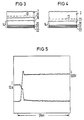
- Zone 15 is contacted by a drain contact 14, the structure of which is described in connection with FIGS. 3 and 4.
- the contact can be produced by sputtering on an aluminum layer 18, which is partially alloyed into the semiconductor body 2.
- An aluminum-silicon alloy 19 is formed which, with appropriate process control, does not penetrate to the pn junction 13. This can e.g. B. can be achieved by heating to 450 ° C for 30 minutes.
- the aluminum layer 18 can then be provided in a known manner with a multilayer contact, which consists, for example, of a titanium layer 20, a nickel layer 21 and a silver layer 22.
- the contact 14 can also be connected to the semiconductor body via a metal silicide.
- a metal silicide for this, z. B. a layer of platinum is applied to the surface 4 of the semiconductor body, then a platinum silicide layer 23 is formed by annealing.
- the process can be controlled by sputtering on a correspondingly thin platinum layer so that after temperature treatment at 450 to 470 ° C. for about 1 h, the platinum silicide layer 23 does not reach the pn junction 13.
- the platinum-silicide layer 23 can then be contacted in a manner similar to that in FIG. 3 by means of a multilayer contact 20, 21, 22.
- FIG. 5 shows the shutdown current I and the voltage U against the shutdown time t in an IGBT of the invention. It can be seen that the loss work is very small. In the example shown, it is approximately 0.68 mWs.
- the invention has been described using an n-channel IGBT. It can of course also be used for p-channel IGBT, in which an n+ zone is used instead of a p+ zone 15. This can e.g. B. by implantation of phosphorus ions. A multilayer contact can then be applied again, which consists, for example, of platinum silicide, titanium, nickel, silver.
Landscapes
- Bipolar Transistors (AREA)
- Thyristors (AREA)
- Insulated Gate Type Field-Effect Transistor (AREA)
Abstract
Description
- Die Erfindung bezieht sich auf einen durch Feldeffekt steuerbaren Bipolartransistor mit einem Halbleiterkörper mit einer Innenzone und einer drainseitigen Zone höherer Dotierung als die Innenzone und vom entgegengesetzten Leitungstyp.
- Solche Bipolartransistoren sind z. B. in dem Artikel "COMFET-THE ULTIMATE POWER DEVICE" in der Zeitschrift "SOLID STATE TECHNOLOGY", November 1985, Seite 121 bis 128 beschrieben worden. Es ist sourceseitig wie ein Leistungs-MOSFET aufgebaut, hat jedoch anodenseitig eine vierte Zone, die den entgegengesetzten Leitungstyp wie die Innenzone aufweist. Es hat somit eine Thyristorstruktur und ist katodenseitig mit einem Nebenschluß versehen, der den vom Thyristor her bekannten sogenannten Einraststrom so erhöht, daß dieser bei Betriebsbedingungen des Bauelements nicht erreicht wird. Am Stromtransport sind hier wie beim Thyristor, aber im Gegensatz zum Leistungs-MOSFET, beide Arten von Ladungsträgern beteiligt. Das bringt einerseits den Vorteil eines niedrigen Durchlaßwiderstandes, andererseits aber den Nachteil einer Sperrverzögerungsladung, die sich beim Abschalten in einem sogenannten "Tail-Strom" bemerkbar macht. Dieser verzögert das Abschalten.
- Die Speicherladung wurde nach verschiedenen Vorschlägen z. B. von Rekombinationszentren oder durch Bestrahlung erzeugte Störstellen vermindert. Ein weiterer Vorschlag besteht darin, zwischen die Innenzone und die Anodenzone eine Pufferzone einzufügen, die vom gleichen Leitfähigkeitstyp wie die Innenzone ist, jedoch eine höhere Dotierungskonzentration als diese hat (man vergleiche das Kapitel "POWER CONTROL" in der Zeitschrift "ELECTRONIC DESIGN, 12. Januar 1984, Seiten 248 und 249).
- Mit den beschrieben Maßnahmen oder mit einer Kombination beider Maßnahmen läßt sich eine Reduzierung der Sperrverzögerungsladung und damit eine Verringerung der Ausschaltzeit erreichen. Ziel der Erfindung ist eine weitere Verringerung der Speicherladung und Verkürzung der Ausschaltzeit mit einfachen Mitteln.
- Dieses Ziel wird dadurch erreicht, daß die drainseitige Zone kleiner als 1µm dick ist, daß sie mit implantierten Ionen mit einer Dosis zwischen 1 x 10¹² und 1 x 10¹⁵cm⁻² dotiert ist und daß die Lebensdauer der Minoritätsträger in der Innenzone mindestens 10 µs beträgt.
- Weiterbildungen der Erfindung sind Gegenstand der Unteransprüche. Die Erfindung wird anhand von Ausführungsbeispielen in Verbindung mit den Figuren 1 bis 5 näher erläutert. Es zeigen:
- FIG 1 einen Schnitt durch einen IGBT;
- FIG 2 die Dotierung und die Ladungsträgerverteilung im stromführenden Zustand;
- FIG 3 und 4 zwei verschiedene Ausführungsbeispiele der Kontaktierung der drainseitigen Zone;
- FIG 5 den Verlauf des Stroms und der Spannung beim Abschalten.
- Der durch Feldeffekt steuerbare Bipolartransistor nach FIG 1, im folgenden IGBT (Isolated Gate Bipolar Transistor) genannt, hat einen Halbleiterkörper 1 mit einer n-dotierten Innenzone 2. Die Dotierung liegt z. B. bei 1-2 x 10¹⁴cm⁻³. Der Halbleiterkörper hat eine sourceseitige Oberfläche 3 und eine drainseitige Oberfläche 4. Die Innenzone 2 reicht bis an die sourceseitige Oberfläche 3. Angrenzend an diese Oberfläche sind in die Innenzone 2 Basiszonen 5 eingebettet, die stark p-dotiert sind. Sie bilden mit der Innenzone pn-Übergänge 12. In jede Basiszone 5 ist eine stark n-dotierte Sourcezone 6 eingebettet. Ihre Dotierung ist höher als die der Basiszonen 5. Auf der Oberfläche 3 sitzt eine Isolierschicht 7, auf der einander parallel geschaltete Gateelektroden 8 angeordnet sind. Die Gateelektroden überdecken einen an die Oberfläche 3 tretenden Teil der Basiszonen 5 und bilden dort Kanalzonen 11. Die Gateelektroden 8 sind von einer weiteren Isolierschicht 9 bedeckt. In den Isolierschichten 7 und 9 Öffnungen vorgesehen, durch die die Sourcezonen 6 und die Basiszonen 5 von einer auf der Isolierschicht 9 liegenden Sourceelektrode 10 kontaktiert sind. Diese besteht vorzugsweise aus Aluminium. Die gemeinsame Kontaktierung der Zonen 5 und 6 durch den Sourcekontakt 10 stellt einen starken Nebenschluß dar.
- Drainseitig schließt sich an die Innenzone 2 eine p-Schicht 15 an. Sie ist wesentlich höher dotiert als die Innenzone 2. Zwischen der drainseitigen Zone 15 und der Innenzone 2 liegt ein pn-Übergang 13. Die Zone 15 ist mit einer Drainelektrode 14 kontaktiert.
- Die drainseitige Zone hat eine Dicke von kleiner 1µm, vorzugsweise 0,1 µm. Sie wird auf bekannte Weise z. B. durch eine Bor-Ionenimplantation mit einer Dosis zwischen 1 x 10¹² und 1 x 10¹⁵, vorzugsweise zwischen 1 x 10¹³ und 1 x 10¹⁴cm⁻² und einer Energie von 45 keV hergestellt. Werden andere Ionen implantiert, so wird die Energie derart eingestellt, daß sich die oben erwähnte Eindringtiefe ergibt. Das Silizium des Halbleiterkörpers is derart beschaffen, daß sich in der Innenzone 2 eine Lebensdauer der aus den Zonen 5 und 15 stammenden Minoritätsladungsträger von mindestens 10µs ergibt. Diese Bedingung ist im allgemeinen ohne weiteres bereits dadurch zu erfüllen, daß der Halbleiterkörper von einem herkömmlichen Zonen- oder tiegelgezogenen Silizium-Monokristallstab abgetrennt und bei seiner Weiterverarbeitung nicht zusätzlich mit Rekombinationszentren bildenden Stoffen dotiert wird. Die genannte Lebensdauer ist z. B. für einen für 1000 V Sperrspannung ausgelegten IGBT mit einer Innenzonendicke von z. B. 200µm so groß, daß in der Innenzone nur eine verschwindend geringe Rekombination von Ladungsträgern stattfindet. Die Lebensdauer kann aber auch wesentlich höher liegen, z. B. in der Größenordnung 100µs. 10µs reicht aber bei 200 µm Dicke aus, da die Laufzeit nur bei etwa 2µs liegt.
- Das Schaubild in FIG 2 zeigt ausgezogen den Dotierungsverlauf und strichpunktiert die Konzentration der freien Ladungsträger im Durchlaßfall. Die Dotierung in der Innenzone 2 ist konstant und durch die Grunddotierung des Halbleitermaterials gegeben.
- Die Zone 15 hat eine um mehrere Zehnerpotenzen höhere Randkonzentration, ebenso jede Basiszone 5. Während die Basiszone 5 z. B. durch Ionenimplantation und anschließendes Eindiffundieren erzeugt werden kann, wird die Zone 15 lediglich durch Implantieren von Ionen ohne nachfolgende Eindiffusion hergestellt. Es wird danach lediglich eine Temperaturbehandlung unter 600 °C durchgeführt, bei der der Dotierstoff noch nicht wesentlich in den Halbleiterkörper eindiffundiert. Anstelle der Temperaturbehandlung unter 600°C kann auch das RTA (Rapid Temperature Annealing) mittels Laser- oder Lichtblitz angewendet werden. Mit beiden Verfahren wird nur ein Teil der durch die Ionenimplantation erzeugten Kristallgitterschäden ausgeheilt. Dies führt zusammen mit der äußerst geringen Dicke der Zone 15 zu einer sehr geringen Emitter-Gummelzahl (Quotient aus Emitterladung und Emitter-Diffusions-konstante) und dadurch zu einem geringen Emitterwirkungsgrad der Zone 15. Damit ist die Anhebung der Minoritätsladungsträger über die Grunddotierung in der Innenzone 2 relativ gering (Punkt A). Da die Innenzone 2 jedoch sehr wenig, d. h. keine zusätzlichen Rekombinationszentren aufweist, fällt die Dichte der freien Ladungsträger (p=n in FIG. 2) über die Dicke der Innenzone 2 im wesentlichen linear bis zur Dichte Null am sourceseitigen pn-Übergang 12, der stets gesperrt ist (Linie 16 in FIG 1). Die Konzentration der freien Ladungsträger in einem Schnitt unterhalb der Gateelektroden (Linie 24 in FIG 1) unterscheidet sich im Durchlaßfall dadurch, daß die Konzentration der freien Ladungsträger p=n sourceseitig angehoben ist.
- Die Zone 15 wird durch einen Drainkontakt 14 kontaktiert, dessen Aufbau in Verbindung mit FIG 3 und 4 beschrieben wird. So kann der Kontakt beispielsweise durch Aufsputtern einer Aluminiumschicht 18 hergestellt werden, die teilweise in den Halbleiterkörper 2 einlegiert wird. Dabei bildet sich eine Aluminium-Silizium-Legierung 19, die bei entsprechender Prozeßführung nicht bis zum pn-Übergang 13 vordringt. Dies kann z. B. durch Erhitzen auf 450°C für 30 Minuten erreicht werden. Die Aluminiumschicht 18 kann dann auf bekannte Weise mit einem Mehrschichtenkontakt versehen, der beispielsweise aus einer Titanschicht 20, einer Nickelschicht 21 und einer Silberschicht 22 besteht.
- Der Kontakt 14 kann (FIG 4) auch über ein Metall-Silizid mit dem Halbleiterkörper verbunden werden. Hierzu wird z. B. eine Schicht Platin auf die Oberfläche 4 des Halbleiterkörpers aufgebracht, dann wird durch Tempern eine Platin-Silizidschicht 23 gebildet. Hier läßt sich der Prozeß durch Aufsputtern einer entsprechend dünnen Platinschicht so steuern, daß nach Temperaturbehandlung bei 450 bis 470 ° C für ca. 1 h , die Platin-Silizidschicht 23 nicht bis an den pn-Übergang 13 heranreicht. Die Platin-Silizid-Schicht 23 kann dann ähnlich wie in FIG 3 durch einen Mehrschichtenkontakt 20, 21, 22 kontaktiert werden.
- In FIG 5 ist der Abschaltstrom I und die Spannung U gegen die Abschaltzeit t bei einem IGBT der Erfindung dargestellt. Es ist ersichtlich, daß die Verlustarbeit sehr klein ist. Im gezeigten Beispiel beträgt sie ca. 0,68 mWs.
Die Erfindung wurde anhand eines n-Kanal-IGBT beschrieben. Sie kann selbstverständlich auch für p-Kanal-IGBT eingesetzt werden, bei dem statt einer p⁺-Zone 15 eine n⁺-Zone verwendet wird. Diese kann z. B. durch Implantation von Phosphorionen hergestellt werden. Anschließend kann wieder ein mehrschichtiger Kontakt aufgebracht werden, der z.B. aus Platinsilizid, Titan, Nickel, Silber besteht.
Claims (7)
Applications Claiming Priority (2)
| Application Number | Priority Date | Filing Date | Title |
|---|---|---|---|
| DE3805799 | 1988-02-24 | ||
| DE3805799 | 1988-02-24 |
Publications (2)
| Publication Number | Publication Date |
|---|---|
| EP0330122A1 true EP0330122A1 (de) | 1989-08-30 |
| EP0330122B1 EP0330122B1 (de) | 1995-10-25 |
Family
ID=6348078
Family Applications (1)
| Application Number | Title | Priority Date | Filing Date |
|---|---|---|---|
| EP89102916A Expired - Lifetime EP0330122B1 (de) | 1988-02-24 | 1989-02-20 | Verfahren zur Herstellung eines durch Feldeffekt steuerbaren Bipolartransistors |
Country Status (4)
| Country | Link |
|---|---|
| US (1) | US4893165A (de) |
| EP (1) | EP0330122B1 (de) |
| JP (1) | JPH0648729B2 (de) |
| DE (1) | DE58909474D1 (de) |
Cited By (10)
| Publication number | Priority date | Publication date | Assignee | Title |
|---|---|---|---|---|
| EP0363673A1 (de) * | 1988-09-15 | 1990-04-18 | Nippondenso Co., Ltd. | Durch Zerstäubung abgeschiedene Nickelschicht und Verfahren zu deren Abscheidung |
| EP0501342A3 (en) * | 1991-03-01 | 1993-03-10 | Fuji Electric Co., Ltd. | Insulated gate bipolar transistor and method of producing same |
| EP0621640A1 (de) * | 1993-04-22 | 1994-10-26 | ABB Management AG | Leistungshalbleiterbauelement |
| US5360765A (en) * | 1991-07-17 | 1994-11-01 | Nippondenso Co., Ltd. | Method of forming electrodes of semiconductor device |
| DE19506386A1 (de) * | 1994-02-24 | 1995-08-31 | Mitsubishi Electric Corp | Halbleiterbauelement und Verfahren zu dessen Herstellung |
| EP0657941A3 (de) * | 1993-12-08 | 1995-10-25 | Siemens Ag | Steuerbares Leistungshalbleiterbauelement mit Pufferzone und Verfahren zu dessen Herstellung. |
| DE19731495A1 (de) * | 1997-07-22 | 1999-01-28 | Siemens Ag | Durch Feldeffekt steuerbarer Bipolartransistor und Verfahren zu seiner Herstellung |
| EP0969501A1 (de) * | 1998-07-02 | 2000-01-05 | Semikron Elektronik GmbH | Verfahren zur Herstellung von Leistungshalbleiterbauelementen |
| DE19832225A1 (de) * | 1998-07-17 | 2000-01-20 | Semikron Elektronik Gmbh | Vierquadrantenumrichter für mittlere und höhere Spannungen |
| EP2637210A1 (de) * | 2012-03-05 | 2013-09-11 | ABB Technology AG | Leistungshalbleiterbauelement und Verfahren zu seiner Herstellung |
Families Citing this family (26)
| Publication number | Priority date | Publication date | Assignee | Title |
|---|---|---|---|---|
| JPH0768460B2 (ja) * | 1987-10-02 | 1995-07-26 | 三菱化学株式会社 | 含金属インドアニリン系化合物および該化合物を用いた光学記録媒体 |
| EP0313000B1 (de) * | 1987-10-21 | 1998-05-06 | Siemens Aktiengesellschaft | Verfahren zum Herstellen eines Bipolartransistors mit isolierter Gateelektrode |
| JP2526653B2 (ja) * | 1989-01-25 | 1996-08-21 | 富士電機株式会社 | 伝導度変調型mosfet |
| JPH02312280A (ja) * | 1989-05-26 | 1990-12-27 | Mitsubishi Electric Corp | 絶縁ゲート型バイポーラトランジスタ |
| JP2890519B2 (ja) * | 1989-09-08 | 1999-05-17 | 富士電機株式会社 | 伝導度変調型mosfetの製造方法 |
| US5005061A (en) * | 1990-02-05 | 1991-04-02 | Motorola, Inc. | Avalanche stress protected semiconductor device having variable input impedance |
| JPH0548111A (ja) * | 1991-08-12 | 1993-02-26 | Toshiba Corp | 半導体装置およびその製造方法 |
| JP2984478B2 (ja) * | 1992-08-15 | 1999-11-29 | 株式会社東芝 | 伝導度変調型半導体装置及びその製造方法 |
| DE69434268T2 (de) * | 1994-07-14 | 2006-01-12 | Stmicroelectronics S.R.L., Agrate Brianza | Intergrierte Struktur einer Hochgeschwindigkeits-MOS-Technologe-Leistungsvorrichtung und zugehöriges Herstellungsverfahren |
| JP3228093B2 (ja) * | 1995-06-28 | 2001-11-12 | 富士電機株式会社 | 高耐圧ic |
| US5589408A (en) * | 1995-07-05 | 1996-12-31 | Motorola, Inc. | Method of forming an alloyed drain field effect transistor and device formed |
| EP0817274B1 (de) | 1996-07-05 | 2004-02-11 | STMicroelectronics S.r.l. | Asymmetrische MOS-Technologie-Leistungsanordnung |
| WO2000035021A1 (de) * | 1998-12-04 | 2000-06-15 | Infineon Technologies Ag | Leistungshalbleiterschalter |
| DE19860581A1 (de) * | 1998-12-29 | 2000-07-06 | Asea Brown Boveri | Halbleiterelement und Verfahren zur Herstellung |
| US6557554B1 (en) | 1999-10-29 | 2003-05-06 | Suzuki Motor Corporation | High-frequency oscillation artificial respiration apparatus |
| JP3727827B2 (ja) * | 2000-05-15 | 2005-12-21 | 株式会社東芝 | 半導体装置 |
| JP4904612B2 (ja) * | 2000-05-22 | 2012-03-28 | 富士電機株式会社 | Igbt |
| JP2001358328A (ja) * | 2000-06-13 | 2001-12-26 | Nippon Inter Electronics Corp | サイリスタ及びそのサイリスタを使用した制御回路 |
| JP4750933B2 (ja) | 2000-09-28 | 2011-08-17 | 株式会社東芝 | 薄型パンチスルー型パワーデバイス |
| US6815767B2 (en) * | 2001-02-01 | 2004-11-09 | Mitsubishi Denki Kabushiki Kaisha | Insulated gate transistor |
| CN100416858C (zh) * | 2001-02-01 | 2008-09-03 | 三菱电机株式会社 | 半导体器件 |
| JP5160001B2 (ja) * | 2001-04-02 | 2013-03-13 | 富士電機株式会社 | 半導体装置の製造方法 |
| DE10250575B4 (de) | 2002-10-30 | 2010-04-15 | Infineon Technologies Ag | IGBT mit monolithisch integrierter antiparalleler Diode |
| JP2005057235A (ja) | 2003-07-24 | 2005-03-03 | Mitsubishi Electric Corp | 絶縁ゲート型バイポーラトランジスタ及びその製造方法、並びに、インバータ回路 |
| JP2008311301A (ja) * | 2007-06-12 | 2008-12-25 | Sanyo Electric Co Ltd | 絶縁ゲートバイポーラトランジスタ |
| JP5445563B2 (ja) * | 2011-11-21 | 2014-03-19 | 富士電機株式会社 | 半導体装置の製造方法 |
Citations (2)
| Publication number | Priority date | Publication date | Assignee | Title |
|---|---|---|---|---|
| GB2088631A (en) * | 1980-12-02 | 1982-06-09 | Gen Electric | Field effect controlled semiconductor rectifier |
| EP0148065A2 (de) * | 1983-12-14 | 1985-07-10 | FAIRCHILD CAMERA & INSTRUMENT CORPORATION | Hochgeschwindigkeits-Halbleiteranordnung, insbesondere eine Hochspannungs-PIN-Diode |
Family Cites Families (6)
| Publication number | Priority date | Publication date | Assignee | Title |
|---|---|---|---|---|
| FR2507820A1 (fr) * | 1981-06-16 | 1982-12-17 | Thomson Csf | Transistor bipolaire a commande par effet de champ au moyen d'une grille isolee |
| US4443931A (en) * | 1982-06-28 | 1984-04-24 | General Electric Company | Method of fabricating a semiconductor device with a base region having a deep portion |
| US4466176A (en) * | 1982-08-09 | 1984-08-21 | General Electric Company | Process for manufacturing insulated-gate semiconductor devices with integral shorts |
| US4620211A (en) * | 1984-08-13 | 1986-10-28 | General Electric Company | Method of reducing the current gain of an inherent bipolar transistor in an insulated-gate semiconductor device and resulting devices |
| US4779123A (en) * | 1985-12-13 | 1988-10-18 | Siliconix Incorporated | Insulated gate transistor array |
| US4821095A (en) * | 1987-03-12 | 1989-04-11 | General Electric Company | Insulated gate semiconductor device with extra short grid and method of fabrication |
-
1989
- 1989-02-20 JP JP1040124A patent/JPH0648729B2/ja not_active Expired - Lifetime
- 1989-02-20 EP EP89102916A patent/EP0330122B1/de not_active Expired - Lifetime
- 1989-02-20 DE DE58909474T patent/DE58909474D1/de not_active Expired - Lifetime
- 1989-02-21 US US07/313,045 patent/US4893165A/en not_active Expired - Lifetime
Patent Citations (2)
| Publication number | Priority date | Publication date | Assignee | Title |
|---|---|---|---|---|
| GB2088631A (en) * | 1980-12-02 | 1982-06-09 | Gen Electric | Field effect controlled semiconductor rectifier |
| EP0148065A2 (de) * | 1983-12-14 | 1985-07-10 | FAIRCHILD CAMERA & INSTRUMENT CORPORATION | Hochgeschwindigkeits-Halbleiteranordnung, insbesondere eine Hochspannungs-PIN-Diode |
Non-Patent Citations (1)
| Title |
|---|
| IEEE TRANSACTIONS ON ELECTRON DEVICES, Band ED-33; Nr. 9, September 1986, Seiten 1377-1382, IEEE, New York, US; J.G. FOSSUM et al.: "Charge-control analysis of the COMFET turn-off transient" * |
Cited By (23)
| Publication number | Priority date | Publication date | Assignee | Title |
|---|---|---|---|---|
| EP0363673A1 (de) * | 1988-09-15 | 1990-04-18 | Nippondenso Co., Ltd. | Durch Zerstäubung abgeschiedene Nickelschicht und Verfahren zu deren Abscheidung |
| US5876861A (en) * | 1988-09-15 | 1999-03-02 | Nippondenso Company, Ltd. | Sputter-deposited nickel layer |
| US6072199A (en) * | 1991-03-01 | 2000-06-06 | Fuji Electric Co., Ltd. | Insulated gate bipolar transistor |
| EP0501342A3 (en) * | 1991-03-01 | 1993-03-10 | Fuji Electric Co., Ltd. | Insulated gate bipolar transistor and method of producing same |
| US5360765A (en) * | 1991-07-17 | 1994-11-01 | Nippondenso Co., Ltd. | Method of forming electrodes of semiconductor device |
| EP0621640A1 (de) * | 1993-04-22 | 1994-10-26 | ABB Management AG | Leistungshalbleiterbauelement |
| DE4313170A1 (de) * | 1993-04-22 | 1994-10-27 | Abb Management Ag | Leistungshalbleiterbauelement |
| EP0657941A3 (de) * | 1993-12-08 | 1995-10-25 | Siemens Ag | Steuerbares Leistungshalbleiterbauelement mit Pufferzone und Verfahren zu dessen Herstellung. |
| US5466951A (en) * | 1993-12-08 | 1995-11-14 | Siemens Aktiengesellschaft | Controllable power semiconductor element with buffer zone and method for the manufacture thereof |
| US5506153A (en) * | 1993-12-08 | 1996-04-09 | Siemens Aktiengesellschaft | Method for manufacture of a controllable power semiconductor element with buffer zone |
| DE19506386A1 (de) * | 1994-02-24 | 1995-08-31 | Mitsubishi Electric Corp | Halbleiterbauelement und Verfahren zu dessen Herstellung |
| DE19506386C2 (de) * | 1994-02-24 | 2003-08-14 | Mitsubishi Electric Corp | Halbleiterbauelement mit in Gräben angeordneten Steuerelektrodenschichten und Verfahren zu dessen Herstellung |
| WO1999005713A1 (de) * | 1997-07-22 | 1999-02-04 | Siemens Aktiengesellschaft | Durch feldeffekt steuerbarer bipolartransistor und verfahren zu seiner herstellung |
| DE19731495C2 (de) * | 1997-07-22 | 1999-05-20 | Siemens Ag | Durch Feldeffekt steuerbarer Bipolartransistor und Verfahren zu seiner Herstellung |
| US6309920B1 (en) | 1997-07-22 | 2001-10-30 | Siemens Aktiengesellschaft | Bipolar transistor which can be controlled by field effect and method for producing the same |
| DE19731495A1 (de) * | 1997-07-22 | 1999-01-28 | Siemens Ag | Durch Feldeffekt steuerbarer Bipolartransistor und Verfahren zu seiner Herstellung |
| EP0969501A1 (de) * | 1998-07-02 | 2000-01-05 | Semikron Elektronik GmbH | Verfahren zur Herstellung von Leistungshalbleiterbauelementen |
| DE19829614A1 (de) * | 1998-07-02 | 2000-01-13 | Semikron Elektronik Gmbh | Verfahren zur Herstellung eines Leistungshalbleiterbauelementes |
| DE19829614B4 (de) * | 1998-07-02 | 2004-09-23 | Semikron Elektronik Gmbh | Verfahren zur Herstellung eines Leistungshalbleiterbauelementes |
| DE19832225A1 (de) * | 1998-07-17 | 2000-01-20 | Semikron Elektronik Gmbh | Vierquadrantenumrichter für mittlere und höhere Spannungen |
| DE19832225C2 (de) * | 1998-07-17 | 2003-03-20 | Semikron Elektronik Gmbh | Vierquadrantenumrichter für mittlere und höhere Spannungen |
| EP2637210A1 (de) * | 2012-03-05 | 2013-09-11 | ABB Technology AG | Leistungshalbleiterbauelement und Verfahren zu seiner Herstellung |
| WO2013131821A1 (en) | 2012-03-05 | 2013-09-12 | Abb Technology Ag | Power semiconductor device and method for manufacturing thereof |
Also Published As
| Publication number | Publication date |
|---|---|
| DE58909474D1 (de) | 1995-11-30 |
| JPH0648729B2 (ja) | 1994-06-22 |
| US4893165A (en) | 1990-01-09 |
| JPH027569A (ja) | 1990-01-11 |
| EP0330122B1 (de) | 1995-10-25 |
Similar Documents
| Publication | Publication Date | Title |
|---|---|---|
| EP0330122B1 (de) | Verfahren zur Herstellung eines durch Feldeffekt steuerbaren Bipolartransistors | |
| DE10217610B4 (de) | Metall-Halbleiter-Kontakt, Halbleiterbauelement, integrierte Schaltungsanordnung und Verfahren | |
| DE102007030805B4 (de) | Halbleitervorrichtung und Herstellungsverfahren derselben | |
| DE10330571B4 (de) | Vertikales Leistungshalbleiterbauelemente mit Injektionsdämpfungsmittel im Randbereich und Herstellungsverfahren dafür | |
| DE102007019561B4 (de) | Halbleitervorrichtung und Herstellungsverfahren derselben | |
| DE102004012818B3 (de) | Verfahren zum Herstellen eines Leistungshalbleiterbauelements | |
| DE2944913A1 (de) | Solarzelle mit amorphem siliziumkoerper | |
| DE102008003953A1 (de) | Verfahren zur Herstellung eines Halbleiterelements | |
| DE112013001297B4 (de) | Verfahren zur Herzustellung einer Leistungshalbleitervorrichtung | |
| DE102005043913B4 (de) | Verfahren zur Herstellung einer dotierten Zone in einem Halbleiterkörper | |
| DE2805442A1 (de) | Verfahren zum herstellen eines schottky-sperrschicht-halbleiterbauelementes | |
| DE2160427B2 (de) | Verfahren zur Herstellung eines Halbleiterwiderstandes mit implantierten Ionen eines neutralen Dotierungsstoffes | |
| EP0071916B1 (de) | Leistungs-MOS-Feldeffekttransistor und Verfahren zu seiner Herstellung | |
| EP1017093B1 (de) | Leistungshalbleiterelement und Verfahren zur Herstellung | |
| EP0014435B1 (de) | Thyristor mit Steuerung durch Feldeffekttransistor | |
| DE10248205B4 (de) | Ohmsche Kontaktanordnung und Herstellverfahren | |
| DE3733100C3 (de) | Abschalt-Thyristor | |
| DE3888462T2 (de) | Verfahren zur Herstellung einer gegen Überspannungen selbst-geschützten Halbleiteranordnung. | |
| DE3011952A1 (de) | Sperrfreier niederohmiger kontakt auf iii-v-halbleitermaterial | |
| EP1097480A1 (de) | Leistungshalbleiterelement mit einem emitterbereich, dem eine stoppzone vorgelagert ist | |
| EP0313000B1 (de) | Verfahren zum Herstellen eines Bipolartransistors mit isolierter Gateelektrode | |
| DE10261424B3 (de) | Verfahren zum Herstellen eines Emitters mit niedrigem Emitterwirkungsgrad | |
| DE102009051317B4 (de) | Verfahren zur Herstellung eines Halbleiterbauelement | |
| EP0315145A1 (de) | Leistungs-Halbleiterbauelement mit vier Schichten | |
| DE10245089A1 (de) | Dotierverfahren und Halbleiterbauelement |
Legal Events
| Date | Code | Title | Description |
|---|---|---|---|
| PUAI | Public reference made under article 153(3) epc to a published international application that has entered the european phase |
Free format text: ORIGINAL CODE: 0009012 |
|
| AK | Designated contracting states |
Kind code of ref document: A1 Designated state(s): CH DE FR GB IT LI SE |
|
| 17P | Request for examination filed |
Effective date: 19890925 |
|
| 17Q | First examination report despatched |
Effective date: 19910527 |
|
| GRAA | (expected) grant |
Free format text: ORIGINAL CODE: 0009210 |
|
| AK | Designated contracting states |
Kind code of ref document: B1 Designated state(s): CH DE FR GB IT LI SE |
|
| REF | Corresponds to: |
Ref document number: 58909474 Country of ref document: DE Date of ref document: 19951130 |
|
| REG | Reference to a national code |
Ref country code: CH Ref legal event code: NV Representative=s name: SIEMENS-ALBIS AKTIENGESELLSCHAFT |
|
| ITF | It: translation for a ep patent filed | ||
| ET | Fr: translation filed | ||
| GBT | Gb: translation of ep patent filed (gb section 77(6)(a)/1977) |
Effective date: 19960108 |
|
| PLBE | No opposition filed within time limit |
Free format text: ORIGINAL CODE: 0009261 |
|
| STAA | Information on the status of an ep patent application or granted ep patent |
Free format text: STATUS: NO OPPOSITION FILED WITHIN TIME LIMIT |
|
| 26N | No opposition filed | ||
| REG | Reference to a national code |
Ref country code: GB Ref legal event code: IF02 |
|
| PGFP | Annual fee paid to national office [announced via postgrant information from national office to epo] |
Ref country code: GB Payment date: 20040130 Year of fee payment: 16 |
|
| PGFP | Annual fee paid to national office [announced via postgrant information from national office to epo] |
Ref country code: CH Payment date: 20040203 Year of fee payment: 16 |
|
| PGFP | Annual fee paid to national office [announced via postgrant information from national office to epo] |
Ref country code: SE Payment date: 20040204 Year of fee payment: 16 |
|
| PG25 | Lapsed in a contracting state [announced via postgrant information from national office to epo] |
Ref country code: GB Free format text: LAPSE BECAUSE OF NON-PAYMENT OF DUE FEES Effective date: 20050220 |
|
| PG25 | Lapsed in a contracting state [announced via postgrant information from national office to epo] |
Ref country code: SE Free format text: LAPSE BECAUSE OF NON-PAYMENT OF DUE FEES Effective date: 20050221 |
|
| PG25 | Lapsed in a contracting state [announced via postgrant information from national office to epo] |
Ref country code: LI Free format text: LAPSE BECAUSE OF NON-PAYMENT OF DUE FEES Effective date: 20050228 Ref country code: CH Free format text: LAPSE BECAUSE OF NON-PAYMENT OF DUE FEES Effective date: 20050228 |
|
| EUG | Se: european patent has lapsed | ||
| APAH | Appeal reference modified |
Free format text: ORIGINAL CODE: EPIDOSCREFNO |
|
| GBPC | Gb: european patent ceased through non-payment of renewal fee |
Effective date: 20050220 |
|
| REG | Reference to a national code |
Ref country code: CH Ref legal event code: PL |
|
| PGFP | Annual fee paid to national office [announced via postgrant information from national office to epo] |
Ref country code: IT Payment date: 20070626 Year of fee payment: 19 |
|
| PGFP | Annual fee paid to national office [announced via postgrant information from national office to epo] |
Ref country code: FR Payment date: 20080214 Year of fee payment: 20 Ref country code: DE Payment date: 20080415 Year of fee payment: 20 |
|
| PG25 | Lapsed in a contracting state [announced via postgrant information from national office to epo] |
Ref country code: IT Free format text: LAPSE BECAUSE OF NON-PAYMENT OF DUE FEES Effective date: 20080220 |