EP0330501A2 - Messanordnung mit automatischer Verstärkungsregelung - Google Patents
Messanordnung mit automatischer Verstärkungsregelung Download PDFInfo
- Publication number
- EP0330501A2 EP0330501A2 EP89301870A EP89301870A EP0330501A2 EP 0330501 A2 EP0330501 A2 EP 0330501A2 EP 89301870 A EP89301870 A EP 89301870A EP 89301870 A EP89301870 A EP 89301870A EP 0330501 A2 EP0330501 A2 EP 0330501A2
- Authority
- EP
- European Patent Office
- Prior art keywords
- signal
- amplifier
- circuit
- light
- receiving element
- Prior art date
- Legal status (The legal status is an assumption and is not a legal conclusion. Google has not performed a legal analysis and makes no representation as to the accuracy of the status listed.)
- Ceased
Links
Images


Classifications
-
- G—PHYSICS
- G01—MEASURING; TESTING
- G01J—MEASUREMENT OF INTENSITY, VELOCITY, SPECTRAL CONTENT, POLARISATION, PHASE OR PULSE CHARACTERISTICS OF INFRARED, VISIBLE OR ULTRAVIOLET LIGHT; COLORIMETRY; RADIATION PYROMETRY
- G01J1/00—Photometry, e.g. photographic exposure meter
- G01J1/10—Photometry, e.g. photographic exposure meter by comparison with reference light or electric value provisionally void
- G01J1/16—Photometry, e.g. photographic exposure meter by comparison with reference light or electric value provisionally void using electric radiation detectors
-
- G—PHYSICS
- G01—MEASURING; TESTING
- G01N—INVESTIGATING OR ANALYSING MATERIALS BY DETERMINING THEIR CHEMICAL OR PHYSICAL PROPERTIES
- G01N21/00—Investigating or analysing materials by the use of optical means, i.e. using sub-millimetre waves, infrared, visible or ultraviolet light
- G01N21/17—Systems in which incident light is modified in accordance with the properties of the material investigated
- G01N21/25—Colour; Spectral properties, i.e. comparison of effect of material on the light at two or more different wavelengths or wavelength bands
- G01N21/27—Colour; Spectral properties, i.e. comparison of effect of material on the light at two or more different wavelengths or wavelength bands using photo-electric detection ; circuits for computing concentration
-
- H—ELECTRICITY
- H03—ELECTRONIC CIRCUITRY
- H03G—CONTROL OF AMPLIFICATION
- H03G3/00—Gain control in amplifiers or frequency changers
- H03G3/20—Automatic control
Definitions
- This invention relates to an automatic gain control circuit (hereunder referred to simply as an AGC circuit) and more particularly to an AGC circuit adapted for an apparatus for measuring a physical quantity relating to energy of light or the like such as a reflectivity (or reflectance) and transmissivity (or transmittance) of an object.
- an AGC circuit adapted for an apparatus for measuring a physical quantity relating to energy of light or the like such as a reflectivity (or reflectance) and transmissivity (or transmittance) of an object.
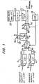
- Fig. 5 shows an AGC circuit of related art adapted for, specially, a sensing circuit for measuring a reflectivity and transmissivity of an object.
- an optical-to-electric (O/E) conversion circuit 2 converts the generated signal into a monitoring signal representing the monitored quantity of light.
- an optical-to-electric conversion circuit 4 converts this signal into another signal of which magnitude is proportional to the measured or observed quantity of light.
- the output signal of the optical-to-electric conversion circuit 4 is inputted into an amplifier 5, an output of which is in turn used to calculate the reflectivity and transmissivity of the object.
- the amplifier 5 is provided with a CdS cell 6 as means for regulating a gain of the AGC circuit.
- the CdS cell 6 comprises a heating element 6a and a temperature detecting resistor 6b. This resistor 6b is connected between an input and output terminals of the optical-to-electric conversion circuit 2.
- an output of the optical-to-electric conversion circuit 2 is inputted into an amplifier 7, the amplified output of which is arranged to be applied to the heating element 6a of the CdS cell 6.
- the gain of the amplifier 5 remains constant and further a signal, of which magnitude is proportional to the measured quantity of light, is obtained by the amplifier 5.
- a signal of which magnitude is proportional to the measured quantity of light
- the reduction of the output of the optical-to-electric conversion circuit 2 causes reduction of an output of the amplifier 7 as well as reduction of electric current flowing through the heating element 6a of the CdS cell 6, resulting in increase of the resistance of the temperature detecting resistor 6b.
- the gain of the amplifier 5 increases to make up an amount of the reduction in the output of the optical-to-electric conversion circuit 4.
- the AGC circuit of the related art comprises the amplifier 5 having the CdS cell 6 to which a signal (hereunder sometimes referred to simply as a measuring signal) representing the observed quantity of light and further comprises another amplifier 7.
- a signal hereunder sometimes referred to simply as a monitoring signal representing the monitored quantity of light is applied to the amplifier 7 and thereafter an output of the amplifier 7 is applied to the CdS cell 6, whereby the above described AGC circuit of the related art can control the gain of the amplifier 5 to prevent the change in magnitude of the monitoring signal from effecting an output of the amplifier 5.
- the AGC circuit of the related art has been widely used in not only measurement of a reflectivity and transmissivity of an object but also evaluation of a ratio of quantity of a certain kind of energy issued from a source to quantity of another kind of energy converted therefrom.
- it is necessary but very difficult to equalize the amplifiers 5 and 7 with each other in all characteristics thereof to improve the precision of measurement. Practically, it is impossible to equalize the amplifiers in temperature coefficient and drift.
- the AGC circuit of the related art has encountered a problem that the precision of measurement is limited below a certain undesirable value due to the variation in characteristics of the amplifiers.
- the present invention is accomplished to resolve the above described problem of the related art.
- an AGC circuit wherein a first signal representing a physical quantity to be measured and a second signal used to control the gain of an amplifier for amplifying the first signal are separately inputted with a predetermined interval of time into the amplifier, the gain of which is controlled or regulated by using a signal outputted from the amplifier at the time of inputting the second signal thereinto, and the first signal is amplified by the amplifier and further the amplified signal is outputted therefrom, with the regulated gain remaining constant.
- an AGC circuit comprising an input terminal means for receiving a first and second signals, an amplifier for receiving and amplifying a first and second signals and outputting a first output signal when receives the first signal and outputting a second output signal when receives the second signals, input means for receiving an operation control signal and responsive to the operation control signal for separately inputting the first and second signals to the amplifier with a predetermined interval of time, control signal generating means responsive to a second output signal of the amplifier for generating a control signal, selection means connected to the input means for supplying the second output signal of the amplifier to the control signal generating means when the second signal is fed to the amplifier and sending out the first output signals to an external circuit when the first signal is fed to the amplifier and gain control means connected to the amplifier and the control signal generating means and responsive to the control signal for regulating the gain of the amplifier, wherein the control signal generating means includes gain maintaining means for maintaining the regulated gain of the amplifier.
- the physical quantity such as a reflectivity being measured by the apparatus provided with the AGC circuit of the present invention can be substantially free from effects of change in temperature characteristics and drift characteristics of the amplifier of the AGC circuit.
- the apparatus provided with the AGC circuit of the present invention can effect measurement of a physical quantity more precisely than the related art does.
- Fig. 1 shows the AGC circuit pursuant to the present invention which is applied to a sensing circuit for measuring a reflectivity and transmissivity of an object.
- like reference characters indicate like elements shown in Fig. 5.
- the AGC circuit shown in this figure is provided with switching circuits 8 and 9, an oscillating circuit 10, a hold circuit 11, a comparator 12 and a reference voltage generating circuit 13 in place of the amplifier 7 shown in Fig. 5.
- the switching circuit 8 is connected to an input portion of the amplifier 5.
- an actuator of the switch 8 When an actuator of the switch 8 is connected to a fixed contact 8a, an output signal S2 of the optical-to-electric conversion circuit 2 is inputted to the amplifier 5.
- an output signal S1 of the optical-to-electric conversion circuit 4 is inputted to the amplifier 5.
- the switching circuit 9 is connected to an output portion of the amplifier 5.
- an actuator When an actuator is connected to a contact 9c, an output signal S3 of the amplifier 5 is supplied to the hold circuit 11. Further, when connected to a contact 9d, the output signal S3 is further sent to an external circuit (not shown) whereupon the output signal 33 is used for calculation of the reflectivity and transmissivity.
- the oscillating circuit 10 is provided in the AGC circuit which is responsive to an operation control signal inputted from a keyboard (not shown) to generate a signal (hereunder referred to simply as a timing signal) which is used to control timing of simultaneously changing the connections in the switching circuits 8 and 9.
- a timing signal hereunder referred to simply as a timing signal
- the switching circuit 8 operates as means for separately inputting at an predetermined interval of time into the amplifier 5 an output signal S2 (hereunder sometimes referred to as a first signal) representing an observed value of a physical quantity to be measured and an output signal S1 (hereunder sometimes referred to a second signal) used for producing a control signal which will be described hereinbelow.
- the switching circuit 9 operates as means for feeding the output signal of the amplifier 5 to means (which will be also described hereinbelow) for producing the control signal when the second signal is supplied to the amplifier 5 and also functions as selection means for sending the output signal of the amplifier 5 to the external circuit when the first signal is supplied to the amplifier 5.
- the hold circuit 11 is adapted to output a signal a very short time later after the time t1, at which the input voltage is removed therefrom, and further adapted to continue outputting the signal thereafter in such a manner that the magnitude of the signal is maintained at the value of immediately before the time t1, as shown in Fig. 2(b).
- the comparing circuit 12 is with two inputs, one of which is an output of the hold circuit 11 and the other of which is an output of the reference voltage generating circuit 13, and is further adapted to issue an output signal to the heating element 6a of the CdS cell 6 in case that the inputs are substantially equal in magnitude with each other.
- the hold circuit 11, the comnparating circuit 12 and the reference voltage circuit 13 operate as means for producing control signals to be used for controlling the gain of the amplifier 5.
- the oscillating circuit 10 synchronously causes the switching circuits 8 and 9 to change the connections therein.
- the signal S1 is amplified by the amplifier 5.
- the amplified signal S3 is outputted from the amplifier 5 and then received by the hold circuit 11.
- the hold circuit 11 outputs to the comparing circuit 12 the voltage corresponding to the input voltage as shown in Figs. 2 (a) and (b). Further, when the output voltage of the hold circuit 11 is equal to that of the reference voltage generating circuit 13, the comparing circuit 12 applies such a voltage to the heating element of the CdS cell 6.
- the gain of the amplifier 5 increases when the output signal S1 of the optical-to-electric conversion circuit 2 is small in magnitude while the gain of the amplifier 5 decreases when the signal S1 from the optical-to-electric conversion circuit 2 increases in magnitude.
- the oscillating circuit 10 causes the actuator of the switching circuit 8 to be connected to the contact 8b at the time t1 and simultaneously causes the actuator of the switching circuit 9 to be connected to the contact 9d
- the input and output voltages of immediately before the time t1 are maintained by the hold circuit 11 after the time t1 as shown in Figs. 2 (a) and (b). Further, the gain of the amplifier 5 is also maintained at the value of immediately before the time t1.
- the output signal S2 of the optical-to-electric conversion circuit 4 is applied to the amplifier 5.
- the output signal S3 of the amplifier 5 is used for calculation of the reflectivity and transmissivity.
- the gain of the amplifier 5 increases (or decreases) in response to increase (or decrease) in magnitude of the signal S2 outputted from the optical-to-electric conversion circuit 4 due to variation in the quantity of light emitted from the source of light.
- the AGC circuit of the present invention can compensate for variation in the observed value of the physical quantity to be measured.
- the gain controllable amplifier compensates for change in the observed value due to variation in characteristics of the amplifier itself. Thereby, it can prevent occurrence of an error in an observed value resulting from differences in characteristics between the amplifiers and further significantly improve the precision of measurement.
- FIG. 3 there is shown another preferred embodiment of the present invention.
- this embodiment is provided with a charge coupled device (CCD) 14, a CCD driving circuit 15 for driving the CCD 14 and a CCD-signal-processing circuit 16 for processing an output signal of the CCD driving circuit and supplying a voltage signal to the amplifier 5, instead of the light receiving elements 1 and 3 and the optical-to-electric conversion circuit 2 and 4 as provided in the embodiment shown in Fig. 1.
- CCD charge coupled device
- FIG. 1 charge coupled device 14
- CCD-signal-processing circuit 16 for processing an output signal of the CCD driving circuit and supplying a voltage signal to the amplifier 5
- a counter 17 for counting output pulses of the oscillator 10 and a reset signal generating circuit 18 responsive to an operation control signal inputted from the keyboard (not shown) for use in resetting the counter 17 and the CCD driving circuit 15, in place of the switching circuit 8 as shown in Fig. 1.
- the CCD driving circuit 15 drives the CCD 14 by using the output pulses of the oscillator 10 and further the counter 17 counts the pulses.
- the monitored quantity of light from the source of light is represented by a specific bit, for example, a first bit indicated by the CCD 14, a second signal representing the monitored quantity of light is outputted therefrom.
- the observed or measured quantity of light from an object to be measured is represented by another bit indicated by the CCD 14 and a first signal representing the measured quantity of light is outputted therefrom.
- the CCD-signal-processing circuit 16 sequentially outputs these signals representing data of the quantity of light as data varying with time which are to be treated in time series.
- the circuit 16 outputs the first and second signals by turns to the amplifier 5.
- the first and second signals are separately supplied to the amplifier 5 at a certain interval of time.
- the counter 17 causes the switching circuit 9 to change the connection therein in accordance with the counted value. That is, the actuator of the switching circuit 9 is connected to the contact 9c at the time of applying the signal representing data indicated by the first bit to the amplifier 5 and is alternatively connected to the contact 9d at the time of applying the signal representing data indicated by the second bit or another one of the remaining bits to the amplifier 5.
- the gain of the amplifier 5 is controlled in response to the monitored quantity of light represented by the second signal in the manner as above described in the explanation of the embodiment of Fig. 1.
- the voltage signal corresponding to the observed quantity of light represented by the first signal outputted from the amplifier 5 of such a gain is provided to the external circuit to calculate the reflectivity and transmissivity of an object.
- the reset signal generating circuit 18 resets the CCD driving circuit 15 such that the driving circuit 15 scans the CCD 14 repeatedly, and simultaneously resets the counter 17.
- the change in the measured or observed quantity of light due to the variation in quantity of light from the source is compensated every period of time of driving the CCD 14.
- this embodiment also compensates the change of the measured quantity of light due to the variation in characteristics of the amplifier by using the amplifier itself, thereby significantly improving the precision of measurement as the former embodiment does.
- the amplifier 5 controls or regulate the gain of the amplifier 5 by maintaining the output of the amplifier 5 by use of the hold circuit 11.
- the amplifier 5 is adapted to amplify the first signal S2 representing the observed quantity of light corresponding to the physical quantity to be measured in such a manner that the regulated gain of the amplifier remains.
- the hold circuit 11 is used as means for maintaining the regulated gain of the amplifier.
- the comparing circuit 12 can be used as means for maintaining the regulated gain of the amplifier because the magnitude of the control signal can remain constant by maintaining that of the output signal thereof.
- the AGC circuit of the present invention is applied to a circuit for measuring the reflectivity and transmissivity of an object. It is our intention that the present invention be not limited by any of the details of description an can be applied to most of the apparatus for using a kind of a source of energy and measuring a ratio of quantity of energy emitted from the source to quantity of another kind of energy converted therefrom.
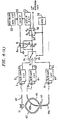
- Figs. 4 (a) and (b) are schematic block diagrams for showing an example of application of the AGC circuit of the present invention, in which like reference characters indicate like elements shown in Fig. 1.
- Fig. 4 (a) shows a sensing circuit for measuring a transmissivity of an object 43
- Fig. 4 (b) shows another sensing circuit for measuring a reflectivity and transmissivity of the object 43.
- the sensing circuit shown in Fig. 4 (a) is provided with a light irradiating portion for irradiating the object 43 by transmitting light radiated from a source 41 of light through an optical fiber 42 to the surface of the object 43, in addition to the elements shown in Fig. 1.
- this sensing circuit another optical fiber 44 is provided for transmitting part of the light from the source 41 to the light receiving element 1 shown in Fig. 1 and still another optical fiber 45 is further provided for transferring light transmitted through the object 43 to the light receiving element 3, whereby a sensing portion of this sensing circuit can be small in size and thus this sensing circuit can be used for measurement of physical quantities of various objects.
- Fig. 4 (b) there is shown another sensing circuit as another example of application of the AGC circuit of the present invention.
- this sensing circuit is different in construction from the sensing circuit of Fig. 4 (a) in that an optical fiber 45a, a light receiving element 3a and an optical-to-electric (O/E) conversion circuit 4a are further provided therein in such a manner to be able to measure a reflectivity of the object 43.
- a switching circuit 8a is not equivalent to the switching circuit 8 and is adapted to receive output signals S1, S2 and S5 of optical-to-electric conversion circuits 2, 4a and 4b.
- the oscillating circuit 10 generates a timing signal for making the switching circuits 8 and 9 to simultaneously change the connections therein.
- the actuator of the switching circuit 8 is connected to the contact 8a
- the actuator of the switching circuit 9 is connected to the contact 9c.
- the actuator of the switching circuit 8 is connected to the contact 8b or 8c
- the actuator of the switching circuit 9 is connected to the contact 9d.
- the sensing circuit of Fig. 4 (b) can be small and used for measurement of the reflectivity and transmissivity of various objects.
Landscapes
- Physics & Mathematics (AREA)
- Spectroscopy & Molecular Physics (AREA)
- General Physics & Mathematics (AREA)
- Analytical Chemistry (AREA)
- Theoretical Computer Science (AREA)
- Health & Medical Sciences (AREA)
- Life Sciences & Earth Sciences (AREA)
- Chemical & Material Sciences (AREA)
- Mathematical Physics (AREA)
- Biochemistry (AREA)
- General Health & Medical Sciences (AREA)
- Engineering & Computer Science (AREA)
- Immunology (AREA)
- Pathology (AREA)
- Investigating Or Analysing Materials By Optical Means (AREA)
- Control Of Amplification And Gain Control (AREA)
Applications Claiming Priority (4)
| Application Number | Priority Date | Filing Date | Title |
|---|---|---|---|
| JP4316688A JPH01218114A (ja) | 1988-02-25 | 1988-02-25 | 自動利得制御回路 |
| JP4316588A JPH01217241A (ja) | 1988-02-25 | 1988-02-25 | 反射率及び透過率測定装置 |
| JP43165/88 | 1988-02-25 | ||
| JP43166/88 | 1988-02-25 |
Publications (2)
| Publication Number | Publication Date |
|---|---|
| EP0330501A2 true EP0330501A2 (de) | 1989-08-30 |
| EP0330501A3 EP0330501A3 (de) | 1991-03-27 |
Family
ID=26382912
Family Applications (1)
| Application Number | Title | Priority Date | Filing Date |
|---|---|---|---|
| EP19890301870 Ceased EP0330501A3 (de) | 1988-02-25 | 1989-02-24 | Messanordnung mit automatischer Verstärkungsregelung |
Country Status (3)
| Country | Link |
|---|---|
| US (1) | US4916406A (de) |
| EP (1) | EP0330501A3 (de) |
| CA (1) | CA1301859C (de) |
Cited By (4)
| Publication number | Priority date | Publication date | Assignee | Title |
|---|---|---|---|---|
| AU630206B2 (en) * | 1989-07-01 | 1992-10-22 | Ericsson Omc Limited | Receiver |
| EP0632679A1 (de) * | 1993-06-22 | 1995-01-04 | Siemens Aktiengesellschaft | Verfahren und Schaltungsanordnung zur Regelung der Beleuchtung eines Raumes |
| EP1087215A3 (de) * | 1999-09-22 | 2004-07-07 | Sick AG | Verfahren zum Betrieb eines optoelektronischen Kontrasttasters |
| WO2013149887A1 (de) * | 2012-04-03 | 2013-10-10 | Osram Gmbh | Lichtsensor für eine beleuchtungseinrichtung, ein beleuchtungssystem umfassend mindestens einen lichtsensor und ein verfahren zur einstellung einer helligkeit eines beleuchtungssystems umfassend mindestens einen lichtsensor |
Families Citing this family (2)
| Publication number | Priority date | Publication date | Assignee | Title |
|---|---|---|---|---|
| JP3003302B2 (ja) * | 1991-07-17 | 2000-01-24 | ソニー株式会社 | 固体撮像素子の信号処理回路及び信号処理方法 |
| US6975172B2 (en) * | 2004-05-03 | 2005-12-13 | Peavey Electronics Corporation | Smart voltage rail reduction audio amplifier |
Family Cites Families (3)
| Publication number | Priority date | Publication date | Assignee | Title |
|---|---|---|---|---|
| US3652944A (en) * | 1969-05-19 | 1972-03-28 | Bunker Ramo | Pulse-characteristic modifying circuit |
| US4040747A (en) * | 1972-08-24 | 1977-08-09 | Neotec Corporation | Optical analyzer for agricultural products |
| DE3406645A1 (de) * | 1984-02-24 | 1985-08-29 | Leybold-Heraeus GmbH, 5000 Köln | Spektralfotometeranordnung |
-
1989
- 1989-02-24 EP EP19890301870 patent/EP0330501A3/de not_active Ceased
- 1989-02-24 CA CA000591953A patent/CA1301859C/en not_active Expired - Lifetime
- 1989-02-27 US US07/316,062 patent/US4916406A/en not_active Expired - Lifetime
Cited By (4)
| Publication number | Priority date | Publication date | Assignee | Title |
|---|---|---|---|---|
| AU630206B2 (en) * | 1989-07-01 | 1992-10-22 | Ericsson Omc Limited | Receiver |
| EP0632679A1 (de) * | 1993-06-22 | 1995-01-04 | Siemens Aktiengesellschaft | Verfahren und Schaltungsanordnung zur Regelung der Beleuchtung eines Raumes |
| EP1087215A3 (de) * | 1999-09-22 | 2004-07-07 | Sick AG | Verfahren zum Betrieb eines optoelektronischen Kontrasttasters |
| WO2013149887A1 (de) * | 2012-04-03 | 2013-10-10 | Osram Gmbh | Lichtsensor für eine beleuchtungseinrichtung, ein beleuchtungssystem umfassend mindestens einen lichtsensor und ein verfahren zur einstellung einer helligkeit eines beleuchtungssystems umfassend mindestens einen lichtsensor |
Also Published As
| Publication number | Publication date |
|---|---|
| US4916406A (en) | 1990-04-10 |
| CA1301859C (en) | 1992-05-26 |
| EP0330501A3 (de) | 1991-03-27 |
Similar Documents
| Publication | Publication Date | Title |
|---|---|---|
| CN1047847C (zh) | 过程控制温度变送器的校准 | |
| US5018154A (en) | Semiconductor laser drive device | |
| US5822369A (en) | Sensor device | |
| CA2475850A1 (en) | Apparatus and method for measurement of dynamic laser signals | |
| US4727382A (en) | Intensity control for a semiconductor laser of a laser beam printer | |
| US4916406A (en) | Automatic gain control circuit | |
| JP2629077B2 (ja) | ランプ電圧発生器の自動較正システム | |
| US5351549A (en) | Pulsed pressure sensor circuit and method therefor | |
| US4616329A (en) | Self-calibrating adaptive ranging apparatus and method | |
| US4097849A (en) | Electronic comparator for process control | |
| US4320289A (en) | Precision laser pulse radiometer | |
| JPH0347020B2 (de) | ||
| US4679940A (en) | Control system for a continuous cell target readout in a laser measurement system | |
| US6414310B1 (en) | Automatic control circuit for infrared detectors | |
| US5012097A (en) | Radiation measuring apparatus | |
| US3796993A (en) | Analog input device for data transmission systems | |
| JPH07209185A (ja) | 表面散乱形濁度計 | |
| JP3253751B2 (ja) | 放電タイミング調整装置 | |
| JPH01218114A (ja) | 自動利得制御回路 | |
| US5134438A (en) | Image forming apparatus having a device for measuring an original density | |
| JPH01229596A (ja) | ディジタル制御装置 | |
| JP2668166B2 (ja) | データ伝送システムにおける端末調整装置 | |
| JPS6052159A (ja) | 光学的画像読み取り装置 | |
| JPS6115476B2 (de) | ||
| JPS643411B2 (de) |
Legal Events
| Date | Code | Title | Description |
|---|---|---|---|
| PUAI | Public reference made under article 153(3) epc to a published international application that has entered the european phase |
Free format text: ORIGINAL CODE: 0009012 |
|
| AK | Designated contracting states |
Kind code of ref document: A2 Designated state(s): DE FR GB NL |
|
| PUAL | Search report despatched |
Free format text: ORIGINAL CODE: 0009013 |
|
| AK | Designated contracting states |
Kind code of ref document: A3 Designated state(s): DE FR GB NL |
|
| 17P | Request for examination filed |
Effective date: 19910703 |
|
| 17Q | First examination report despatched |
Effective date: 19931102 |
|
| STAA | Information on the status of an ep patent application or granted ep patent |
Free format text: STATUS: THE APPLICATION HAS BEEN REFUSED |
|
| 18R | Application refused |
Effective date: 19941205 |