EP0330628B1 - High side driver MOS circuit - Google Patents
High side driver MOS circuit Download PDFInfo
- Publication number
- EP0330628B1 EP0330628B1 EP89830065A EP89830065A EP0330628B1 EP 0330628 B1 EP0330628 B1 EP 0330628B1 EP 89830065 A EP89830065 A EP 89830065A EP 89830065 A EP89830065 A EP 89830065A EP 0330628 B1 EP0330628 B1 EP 0330628B1
- Authority
- EP
- European Patent Office
- Prior art keywords
- circuit
- transistor
- drain
- signal
- gate
- Prior art date
- Legal status (The legal status is an assumption and is not a legal conclusion. Google has not performed a legal analysis and makes no representation as to the accuracy of the status listed.)
- Expired - Lifetime
Links
- 230000000630 rising effect Effects 0.000 claims description 3
- 230000007704 transition Effects 0.000 claims description 3
- 238000010586 diagram Methods 0.000 description 5
- 238000000034 method Methods 0.000 description 3
- 230000006870 function Effects 0.000 description 1
- 230000001172 regenerating effect Effects 0.000 description 1
Images
Classifications
-
- H—ELECTRICITY
- H03—ELECTRONIC CIRCUITRY
- H03K—PULSE TECHNIQUE
- H03K17/00—Electronic switching or gating, i.e. not by contact-making and –breaking
- H03K17/06—Modifications for ensuring a fully conducting state
- H03K17/063—Modifications for ensuring a fully conducting state in field-effect transistor switches
Definitions
- the present invention relates to intergrated MOS circuits and particularly to a circuit for driving a power MOS transistor.
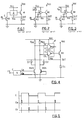
- FIG. 1 An example of a driving circuit of this known type (high side driver in literature) is depicted in Figures 1, 2 and 3.
- the potential difference between the nodes V SS and V GG is maintained constant by means of a suitable voltage generator (a battery or a power supply) while the absolute value of the voltage of nodes V GG and V SS depends on the state (ON or OFF) of the power transistor M1, which switches a supply voltage V DD across the load Zc in function of a driving signal C which is applied to the gate of the driver transistor M2, which may be considered the input terminal IN of the driving circuit.
- a suitable voltage generator a battery or a power supply
- Block 2 of Fig. 1 is essentially an amplifier A, as depicted in Figures 2 and 3.
- the switching OFF and ON of the input transistor M2 causes, by means of the amplifier A, the switching ON and the switching OFF of the power transistor M1.
- a limiting diode D is commonly added in order to protect the input of the amplifier A when the transistor M2 is ON by preventing the potential at the input of the amplifier A to become eccessively negative in respect to the voltage V SS .
- a current generator I (Fig. 2), or a resistor R p (Fig. 3) ensures the maintainance of the drain potential of the transistor M2 at a correct logic level (1) when the transistor is OFF.
- the driving circuits in accordance with the prior art have the disadvantage of dissipating energy during the periods when the transistor M2 is ON and the state of the output transistor M1 is tied to the state of the input transistor M2 of the driving circuit.
- a main objective of the present invention is to provide a driving circuit for a high side driver circuit which dissipates energy only during a transition from one state to another state.
- the driving circuit of the invention as defined by claim 1 is based upon the use of a memory element, in practice a flip-flop, for driving the power transistor by driving the flip-flop, through the respective SET and RESET terminals, by means of two pulse signals derived from a drive switching signal C.
- the first of the pulse signals (C S ) is a pulse coinciding with a trailing edge of the drive switching signal C
- the second derived signal (C R ) is a pulse coinciding with a rise or front edge of the drive switching signal C.
- the memory element F may be constituted by a SET-RESET type flip-flop supplied from the nodes V GG and V SS of the circuit.
- the input SET (S) of the flip-flop is connected to the drain of a first, grounded source, input transistor M2S, and the RESET (R) input of the flip-flop is connected to the drain of a second, grounded source, input transistor M2R.
- a load element (R p1 , and R p2 ) is connected between the drain of each of the two input transistors, respectively, and the node V GG , in order to ensure that the drain potential of the two input transistors is kept at a level corresponding to a stationary logic state 1 when the two transistors are OFF.
- This load element may be, as shown in Fig. 4, a resistor (R p1 and R p2 , respectively) or a current generator.
- a diode (D1 and D2, respectively) is preferably connected between the node V SS (the source or output node of the power switching transistor M1) and the drain of each of the two input transistors M2S and M2R, in order to prevent the drain potential of the two transistors from becoming excessively negative in respect to the V SS when they are conducting.
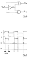
- the two input transistors M2R and M2S are driven by two pulse signals, C R and C S , respectively, the first of which is a pulse which coincides with the rising edge of the drive switching signal C, while the second is a pulse which coincides with the falling edge of the drive switching signal C.
- the pulse signals C R and C S are derived from the switching signal C, which is applied to an input terminal IN of the driving circuit, by means of any suitable circuit means, indicated by the block S in Fig. 4, and which may be made in various forms as it is well known to a skilled technician.
- FIG. 6 A preferred embodiment of such circuit means capable of deriving two positive pulse signals C R and C S from a drive switching signal C is depicted in Fig. 6 and is based on the utilization of the delay introduced by an inverting logic gate (an inverter).
- an inverting logic gate an inverter
- the driving memory element F though being depicted in Fig. 4 as formed by two NAND gates, may also be formed with different logic gates or with any other bistable element having suitable characteristics.
Landscapes
- Logic Circuits (AREA)
- Electronic Switches (AREA)
Applications Claiming Priority (2)
| Application Number | Priority Date | Filing Date | Title |
|---|---|---|---|
| IT83616/88A IT1221251B (it) | 1988-02-25 | 1988-02-25 | Circuito mos per il pilotaggio di un carico dal lato alto della alimentazione |
| IT8361688 | 1988-02-25 |
Publications (3)
| Publication Number | Publication Date |
|---|---|
| EP0330628A2 EP0330628A2 (en) | 1989-08-30 |
| EP0330628A3 EP0330628A3 (en) | 1990-11-22 |
| EP0330628B1 true EP0330628B1 (en) | 1994-01-26 |
Family
ID=11323186
Family Applications (1)
| Application Number | Title | Priority Date | Filing Date |
|---|---|---|---|
| EP89830065A Expired - Lifetime EP0330628B1 (en) | 1988-02-25 | 1989-02-17 | High side driver MOS circuit |
Country Status (5)
| Country | Link |
|---|---|
| US (1) | US4942309A (it) |
| EP (1) | EP0330628B1 (it) |
| JP (1) | JPH029219A (it) |
| DE (1) | DE68912617T2 (it) |
| IT (1) | IT1221251B (it) |
Cited By (2)
| Publication number | Priority date | Publication date | Assignee | Title |
|---|---|---|---|---|
| DE102009037486B3 (de) * | 2009-08-13 | 2011-07-28 | Texas Instruments Deutschland GmbH, 85356 | Elektronische Vorrichtung und Verfahren zur effizienten Pegelverschiebung |
| TWI469482B (zh) * | 2012-03-15 | 2015-01-11 | Univ Nat Chiao Tung | 上橋式驅動電路 |
Families Citing this family (23)
| Publication number | Priority date | Publication date | Assignee | Title |
|---|---|---|---|---|
| JPH0693615B2 (ja) * | 1988-05-16 | 1994-11-16 | 株式会社東芝 | ドライバ回路 |
| JPH0654873B2 (ja) * | 1989-09-04 | 1994-07-20 | 株式会社東芝 | プログラマブル型論理装置 |
| US5007795A (en) * | 1989-10-06 | 1991-04-16 | Yajima Kogyo, Inc. | Supply head of nut feeder |
| USRE36480E (en) * | 1990-01-09 | 2000-01-04 | Stmicroelectronics, S.A. | Control and monitoring device for a power switch |
| FR2656965B1 (fr) * | 1990-01-09 | 1995-01-20 | Sgs Thomson Microelectronics | Commande et controle d'un commutateur de puissance. |
| IT1243692B (it) * | 1990-07-27 | 1994-06-21 | St Microelectronics Srl | Dospositivo per il pilotaggio di un circuito flottante con un segnale digitale |
| US5099148A (en) * | 1990-10-22 | 1992-03-24 | Sgs-Thomson Microelectronics, Inc. | Integrated circuit having multiple data outputs sharing a resistor network |
| IT1251097B (it) * | 1991-07-24 | 1995-05-04 | St Microelectronics Srl | Circuito di bootstrap per il pilotaggio di un transistore mos di potenza in configurazione high side driver. |
| DE4202251C2 (de) * | 1992-01-16 | 2000-01-05 | Rainer Schroecker | Schaltungsanordnung zum Ansteuern von feldgesteuerten Leistungsschaltern |
| DE69403964T2 (de) * | 1994-09-16 | 1998-01-29 | Sgs Thomson Microelectronics | Steuerschaltung mit einem Pegelschieber zum Schalten eines eletronischen Schalters |
| EP0703667B1 (en) * | 1994-09-16 | 1997-06-25 | STMicroelectronics S.r.l. | An integrated control circuit with a level shifter for switching an electronic switch |
| US5543740A (en) * | 1995-04-10 | 1996-08-06 | Philips Electronics North America Corporation | Integrated half-bridge driver circuit |
| EP0764365A2 (en) * | 1995-04-10 | 1997-03-26 | Koninklijke Philips Electronics N.V. | Level-shifting circuit and high-side driver including such a level-shifting circuit |
| EP0746098B1 (en) * | 1995-05-31 | 2003-04-09 | STMicroelectronics S.r.l. | Pulse generator, circuit and method for driving electronic devices, and corresponding applications |
| DE19534701A1 (de) * | 1995-09-19 | 1997-03-20 | Hansjuergen Dipl Phys Dreuth | Bistabiles elektronisches Relais |
| US5719521A (en) * | 1996-10-29 | 1998-02-17 | Philips Electronics North America Corporation | Integrated half-bridge timing control circuit |
| JP3635975B2 (ja) * | 1999-03-02 | 2005-04-06 | 富士電機デバイステクノロジー株式会社 | レベルシフト回路 |
| US6507226B2 (en) * | 2000-07-31 | 2003-01-14 | Intersil Americas Inc. | Power device driving circuit and associated methods |
| JP4382312B2 (ja) * | 2001-09-05 | 2009-12-09 | 三菱電機株式会社 | 駆動制御装置、電力変換装置、電力変換装置の制御方法、および電力変換装置の使用方法 |
| US6809553B2 (en) * | 2001-10-15 | 2004-10-26 | International Rectifier Corporation | Digital level shifter with reduced power dissipation and false transmission blocking |
| EP1919082B1 (en) | 2006-10-30 | 2009-12-02 | Infineon Technologies Austria AG | Circuit arrangement and methods for driving a high-side semiconductor switch |
| WO2008101548A1 (en) * | 2007-02-22 | 2008-08-28 | Mueta B.V. | Level shift circuit |
| CN112953488B (zh) * | 2021-02-20 | 2024-06-25 | 国家超级计算无锡中心 | 基于倍频原理的低功耗高侧驱动电路 |
Family Cites Families (4)
| Publication number | Priority date | Publication date | Assignee | Title |
|---|---|---|---|---|
| US4498021A (en) * | 1982-07-13 | 1985-02-05 | Matsushita Electric Industrial Co., Ltd. | Booster for transmitting digital signal |
| JPS6033872A (ja) * | 1983-08-02 | 1985-02-21 | Mitsubishi Heavy Ind Ltd | 溶接用倣い検出方法及び装置 |
| US4677324A (en) * | 1986-03-21 | 1987-06-30 | Rca Corporation | Fast switch-off circuit for conductivity modulated field effect transistor |
| US4837458A (en) * | 1986-08-22 | 1989-06-06 | Hitachi, Ltd. | Flip-flop circuit |
-
1988
- 1988-02-25 IT IT83616/88A patent/IT1221251B/it active
-
1989
- 1989-02-17 DE DE89830065T patent/DE68912617T2/de not_active Expired - Fee Related
- 1989-02-17 EP EP89830065A patent/EP0330628B1/en not_active Expired - Lifetime
- 1989-02-22 US US07/313,556 patent/US4942309A/en not_active Expired - Lifetime
- 1989-02-25 JP JP1045042A patent/JPH029219A/ja active Pending
Cited By (2)
| Publication number | Priority date | Publication date | Assignee | Title |
|---|---|---|---|---|
| DE102009037486B3 (de) * | 2009-08-13 | 2011-07-28 | Texas Instruments Deutschland GmbH, 85356 | Elektronische Vorrichtung und Verfahren zur effizienten Pegelverschiebung |
| TWI469482B (zh) * | 2012-03-15 | 2015-01-11 | Univ Nat Chiao Tung | 上橋式驅動電路 |
Also Published As
| Publication number | Publication date |
|---|---|
| DE68912617T2 (de) | 1994-05-11 |
| EP0330628A3 (en) | 1990-11-22 |
| US4942309A (en) | 1990-07-17 |
| IT1221251B (it) | 1990-06-27 |
| JPH029219A (ja) | 1990-01-12 |
| DE68912617D1 (de) | 1994-03-10 |
| IT8883616A0 (it) | 1988-02-25 |
| EP0330628A2 (en) | 1989-08-30 |
Similar Documents
| Publication | Publication Date | Title |
|---|---|---|
| EP0330628B1 (en) | High side driver MOS circuit | |
| JP3415241B2 (ja) | 電圧変換器 | |
| EP0576008B1 (en) | Boost voltage generating circuit | |
| US5896045A (en) | Static pulsed cross-coupled level shifter and method therefor | |
| KR100591520B1 (ko) | 감소된 전압 입출력의 3상태 버퍼 및 그 제조 방법 | |
| KR0170514B1 (ko) | 승압 전원을 갖는 반도체 메모리 장치 | |
| US6087852A (en) | Multiplexing a single output node with multiple output circuits with varying output voltages | |
| US7088167B2 (en) | Level conversion for use in semiconductor device | |
| US5124574A (en) | Semiconductor device for generating a voltage higher than power source potential or lower than grounding potential | |
| EP1437815B1 (en) | Power supply voltage selection circuit | |
| EP0055073A1 (en) | Improvements in or relating to electronic clock generators | |
| US5272389A (en) | Level shifter circuit | |
| JP2969346B2 (ja) | 高出力電圧生成用半導体回路 | |
| US4716303A (en) | MOS IC pull-up circuit | |
| EP0388074A1 (en) | Cmos level shifting circuit | |
| EP0459457A2 (en) | Output driver | |
| JPH08265127A (ja) | ゲート回路,及びディジタル集積回路 | |
| JP3052433B2 (ja) | レベルシフト回路 | |
| JP3003404B2 (ja) | 電源選択回路 | |
| US4496852A (en) | Low power clock generator | |
| KR950001992A (ko) | 반도체 트랜지스터로 형성된 논리게이트 회로 | |
| US7161405B2 (en) | Level shift circuit | |
| KR100215761B1 (ko) | 반도체 메모리장치의 레벨 쉬프트회로 | |
| JP3271269B2 (ja) | 出力駆動回路 | |
| JPH11161354A (ja) | 電圧発生回路 |
Legal Events
| Date | Code | Title | Description |
|---|---|---|---|
| PUAI | Public reference made under article 153(3) epc to a published international application that has entered the european phase |
Free format text: ORIGINAL CODE: 0009012 |
|
| AK | Designated contracting states |
Kind code of ref document: A2 Designated state(s): DE FR GB NL SE |
|
| PUAL | Search report despatched |
Free format text: ORIGINAL CODE: 0009013 |
|
| AK | Designated contracting states |
Kind code of ref document: A3 Designated state(s): DE FR GB NL SE |
|
| 17P | Request for examination filed |
Effective date: 19901220 |
|
| 17Q | First examination report despatched |
Effective date: 19930402 |
|
| GRAA | (expected) grant |
Free format text: ORIGINAL CODE: 0009210 |
|
| AK | Designated contracting states |
Kind code of ref document: B1 Designated state(s): DE FR GB NL SE |
|
| PG25 | Lapsed in a contracting state [announced via postgrant information from national office to epo] |
Ref country code: SE Effective date: 19940126 Ref country code: NL Effective date: 19940126 |
|
| REF | Corresponds to: |
Ref document number: 68912617 Country of ref document: DE Date of ref document: 19940310 |
|
| ET | Fr: translation filed | ||
| NLV1 | Nl: lapsed or annulled due to failure to fulfill the requirements of art. 29p and 29m of the patents act | ||
| PLBE | No opposition filed within time limit |
Free format text: ORIGINAL CODE: 0009261 |
|
| STAA | Information on the status of an ep patent application or granted ep patent |
Free format text: STATUS: NO OPPOSITION FILED WITHIN TIME LIMIT |
|
| 26N | No opposition filed | ||
| REG | Reference to a national code |
Ref country code: FR Ref legal event code: D6 |
|
| REG | Reference to a national code |
Ref country code: GB Ref legal event code: IF02 |
|
| PGFP | Annual fee paid to national office [announced via postgrant information from national office to epo] |
Ref country code: GB Payment date: 20020802 Year of fee payment: 14 |
|
| PGFP | Annual fee paid to national office [announced via postgrant information from national office to epo] |
Ref country code: DE Payment date: 20020827 Year of fee payment: 14 |
|
| PGFP | Annual fee paid to national office [announced via postgrant information from national office to epo] |
Ref country code: FR Payment date: 20020828 Year of fee payment: 14 |
|
| PG25 | Lapsed in a contracting state [announced via postgrant information from national office to epo] |
Ref country code: GB Free format text: LAPSE BECAUSE OF NON-PAYMENT OF DUE FEES Effective date: 20030217 |
|
| PG25 | Lapsed in a contracting state [announced via postgrant information from national office to epo] |
Ref country code: DE Free format text: LAPSE BECAUSE OF NON-PAYMENT OF DUE FEES Effective date: 20030902 |
|
| GBPC | Gb: european patent ceased through non-payment of renewal fee | ||
| PG25 | Lapsed in a contracting state [announced via postgrant information from national office to epo] |
Ref country code: FR Free format text: LAPSE BECAUSE OF NON-PAYMENT OF DUE FEES Effective date: 20031031 |
|
| REG | Reference to a national code |
Ref country code: FR Ref legal event code: ST |