EP0330841B1 - Circuit logique comportant une fonction de test - Google Patents
Circuit logique comportant une fonction de test Download PDFInfo
- Publication number
- EP0330841B1 EP0330841B1 EP89101422A EP89101422A EP0330841B1 EP 0330841 B1 EP0330841 B1 EP 0330841B1 EP 89101422 A EP89101422 A EP 89101422A EP 89101422 A EP89101422 A EP 89101422A EP 0330841 B1 EP0330841 B1 EP 0330841B1
- Authority
- EP
- European Patent Office
- Prior art keywords
- input
- output
- circuit
- test
- logic circuit
- Prior art date
- Legal status (The legal status is an assumption and is not a legal conclusion. Google has not performed a legal analysis and makes no representation as to the accuracy of the status listed.)
- Expired - Lifetime
Links
- 238000012360 testing method Methods 0.000 title claims description 150
- 238000000034 method Methods 0.000 description 7
- 238000012546 transfer Methods 0.000 description 4
- 238000013461 design Methods 0.000 description 3
- 238000010586 diagram Methods 0.000 description 3
- 230000006870 function Effects 0.000 description 3
- 238000011161 development Methods 0.000 description 2
- 238000000429 assembly Methods 0.000 description 1
- 239000003990 capacitor Substances 0.000 description 1
- 238000007796 conventional method Methods 0.000 description 1
- 230000008054 signal transmission Effects 0.000 description 1
- 238000010998 test method Methods 0.000 description 1
Images


Classifications
-
- G—PHYSICS
- G01—MEASURING; TESTING
- G01R—MEASURING ELECTRIC VARIABLES; MEASURING MAGNETIC VARIABLES
- G01R31/00—Arrangements for testing electric properties; Arrangements for locating electric faults; Arrangements for electrical testing characterised by what is being tested not provided for elsewhere
- G01R31/28—Testing of electronic circuits, e.g. by signal tracer
- G01R31/317—Testing of digital circuits
- G01R31/3181—Functional testing
- G01R31/3185—Reconfiguring for testing, e.g. LSSD, partitioning
- G01R31/318533—Reconfiguring for testing, e.g. LSSD, partitioning using scanning techniques, e.g. LSSD, Boundary Scan, JTAG
- G01R31/318536—Scan chain arrangements, e.g. connections, test bus, analog signals
-
- G—PHYSICS
- G01—MEASURING; TESTING
- G01R—MEASURING ELECTRIC VARIABLES; MEASURING MAGNETIC VARIABLES
- G01R31/00—Arrangements for testing electric properties; Arrangements for locating electric faults; Arrangements for electrical testing characterised by what is being tested not provided for elsewhere
- G01R31/28—Testing of electronic circuits, e.g. by signal tracer
- G01R31/317—Testing of digital circuits
- G01R31/3181—Functional testing
- G01R31/3185—Reconfiguring for testing, e.g. LSSD, partitioning
- G01R31/318533—Reconfiguring for testing, e.g. LSSD, partitioning using scanning techniques, e.g. LSSD, Boundary Scan, JTAG
- G01R31/318572—Input/Output interfaces
Definitions
- the present invention relates to a logic circuit, and particularly to a logic circuit employing previously prepared macrocells to enable the logic circuit to be tested easily, and having enhanced test-feasibility.
- LSIs based on the macrocell system are used. These LSIs are a kind of custom LSIs.
- the macrocell system uses macrocells each of which is a circuit block comprising a plurality of elements such as transistors, resistors and capacitors to realize a predetermined function such as a RAM and an ALU.
- the macrocells are prepared in advance and registered in, for instance, a data base.
- the macrocells thus prepared are arranged and wired among them manually or with a CAD to design and form an LSI.
- the macrocell system can greatly reduce a developing period and developing costs of a LSI.
- LSI Level Sensitive Scan Design
- FFs flip-flops
- An output signal from the combinational logic circuit is latched by the shift register, output from the integrated circuit via a scan signal output terminal, and compared with an expected value to judge whether or not the integrated circuit has achieved a predetermined function.
- the logic circuit designed and formed according to the macrocell system is tested as a whole by using, for instance, the LSSD method.
- US-A-3 924 144 shows a method of testing by dividing into isolated functional sub-assemblies Test output patterns from the parts are multiplexed to enable output from a single pin IEEE Design and test of computers vol. 3 no. 6, Dec. 1986, p. 26-32 shows macro testing using test interface elements inserted on signals between macros, for serial testing of macros.
- the object of the present invention is to provide an improved logic circuit.
- a logic circuit capable of operation in a test execution mode and in a normal operating mode, said logic circuit comprising: an operational circuit for providing normal operating mode input signals, a plurality of macrocell means for producing normal operating mode output signals, input path means for transferring said normal operating mode input signals to said plurality of macrocell means, and output path means for transferring said normal operating mode output signals to said operational circuit, each of said macrocell means being capable of being independently tested and having a test object portion and input-output circuit means for inputting input test data and for outputting output test data in said test execution mode, said input-output circuit means including: first holding means for holding said input test data, selector circuit means for shutting off said input path means in said test execution mode, for selecting said input test data from said first holding means and for outputting said input test data to said test object portion, said test object portion being responsive to said input test data to perform a test execution and produce said output test data as a result thereof, second holding means for holding said output test data and outputting said output test data externally
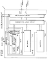
- Fig. 1 is a block diagram showing a logic circuit 1 according to an embodiment of the present invention. In a testing mode, each macrocell can be tested independently from other circuit portions.
- the logic circuit 1 of Fig. 1 has the plurality " l " of macrocells 2(1) to 2( l ), an input-output circuit 3 for receiving input-signals for the logic circuit 1 and generating output-signals for the logic circuit 1, a combinational logic circuit 4 which functions as an interface between the input-output circuit 3 and the macrocells 2(1) to 2( l ) and as a signal transmission path among the macrocells, and a decoder 5 for generating, in the test mode, a select signal for selecting any one of the macrocells 2(1) to 2( l ) or the logic circuit 1 as a whole as a circuit to be tested.
- the input-output circuit 3 receives a signal T/ N ⁇ that specifies a test mode or a normal operation mode, clock signals ⁇ W , ⁇ T , ⁇ E and ⁇ R . Further, the input-output circuit 3 receives, in the test mode, test input data IN.
- the macrocell 2(1) comprises a memory circuit 6 made of many FFs, a combinational logic circuit 7 and an input-output circuit 8.
- Each of the other macrocells 2(2) to 2 ( l ) has the same constitution as that of the macrocell 2(1).
- input signals 101 are given from the outside to the logic circuit 1, and supplied to the input-output circuit 8 in each macrocell.
- Input signals of normal operation mode supplied to the input-output circuit 8 are supplied to the memory circuit 6 via the combinational logic circuit 7.
- Output signals of the memory circuit 6 are given to the input-output circuit 8 via the combinational logic circuit 7.
- Output signals from the input-output circuits 8 are passed through the combinational logic circuit 4 and the input-output circuit 3 and output as output signals 102 of normal operation mode to the outside of the logic circuit 1.
- test input data IN are given from the outside of the logic circuit 1 to the input-output circuit 8 of a macrocell to be tested. Then, the test input data IN are given to the memory circuit 6 via the combinational logic circuit 7. An output from the memory circuit 6 is given to the input-output circuit 8 via the combinational logic circuit 7 and output as test output data OUT from the input-output circuit 8 to the outside of the logic circuit 1.
- test input data IN are given from the outside of the logic circuit 1 to the input-output circuit 3. Then, the test input data IN are given to the respective macrocells 2(1) to 2( l ) through the combinational logic circuit 4, and the output from macrocells are output as test output data OUT through the combinational logic circuit 4 and the input-output circuit 3 to the outside of the logic circuit 1.
- the decoder 5 receives a select signal 103 for selecting a circuit portion to be tested, from the outside of the logic circuit 1 and decodes the select signal 103. And the decoder 5 generates one of the decoded signals 104-0 to 104- l to specify a test object circuit among macrocells 2(1) to 2( l ) and the logic circuit 1.
- the decoder 5 When the logic circuit 1 as a whole is designated as a circuit to be tested by the select signal 103, the decoder 5 outputs a decoded signal 104-0 of signal value 1 to the input-output circuit 3.
- the input-output circuit 3 separates the logic circuit 1 from other circuit portions, receives test input data IN, and outputs the result of process carried out in the logic circuit 1 on the test input data IN as test output data OUT.
- the input-output circuit 8 separates this macrocell 2(i) from the other remaining circuits, transmits the test input data IN to the test object portion in the macrocell 2(i) conists of combinational logic circuit 7 and memory circuit 6, and outputs the result of the operation carried out in the macrocell 2(i) on the test input data IN as test output data OUT.
- Fig. 2 is a view showing the details of the input-output circuit 3 (8).
- the input-output circuits 3 and 8 are similarly constituted.
- Flip-flops FF 11(1) to FF 11(m) constitute a shift register 12.
- the number "m" of stages of the shift register 12 is equal to the number of bits of a first input signal.
- the first input signal is the input signal 101 input from the outside to the logic circuit 1.
- the first input signal is a normal operation mode output signal of the combinational logic circuit 4. Under the test mode the test input data IN are sequentially set to the FFs 11(1) to 11(m), in synchronism with the write clock signal ⁇ W shown in Fig. 3.
- Flip-flops FF 13(1) to FF 13(m) form a shift register 14. Under the test mode each bit value of the test input data IN held in the FF 11(i) is transferred to each FF 13(i) and stored therein in synchronism with the transfer clock signal ⁇ T shown in Fig. 3. The test input data IN written in the shift register 14 are sequentially read out thereof in synchronism with the read clock signal ⁇ R shown in Fig. 3.
- Each of the input-output circuits 3 and 8 has "m" pieces of selectors 15(1) to 15(m).
- Each selector 15(i) receives an "i"th bit of the first input signal as well as an output of the FF 13(i).
- the selector 15(i) selects and outputs the output of the FF 13(i) when the macrocell 2(i) or the logic circuit 1 is designated as a test object circuit and the decoded signal 104-i of logical value 1 is input to the input-output circuit of macrocell 2(i) or of the logic circuit 1 under the test mode.
- the selector 15(i) selects the "i"th bit of the first input signal.
- the "i"th bit of the first input signal or the output of the FF 13(i) thus selected is given to a buffer circuit 16(i).
- the buffer circuits 16(1) to 16(m) output after amplication or block the signals given from the respective selectors, according to a control signal generated in a control signal generating portion (not shown).
- a plurality "n” of FFs 17(1) to 17(n) constitute a shift register 18.
- the number "n” of stages of the shift register 18 is equal to the bit width of a second input signal.
- the second input signal is an output signal of the combinational logic circuit 4.
- the second input signal is an output signal of the combinational logic circuit 7.
- the FF 17(1) in the first stage of the shift register 18 is connected to the FF 13(m) in the last stage of the shift register 14.
- the second input signal is set in the FFs 17(1) to 17(n) under the test mode in synchonism with the execution clock signal ⁇ E shown in Fig. 3. And under the test mode, the shift registers 14 and 18 operates as one continuous shift register , information pieces held in the shift registers 14 and 18 are output as the test output data OUT in synchronism with the read clock signal ⁇ R shown in Fig. 3.
- Each of the input-output circuits 3 and 8 is provided with buffer circuits 19(1) to 19(n).
- the buffer circuits 19(1) to 19(n) receive the decoded signal, and their internal conditions are controlled by the decoded signal. That is when the decoded signal of logical value 1 is input under the test mode, each buffer circuit is put in a high-impedance state to separate the logic circuit 1 or the macrocell as test object circuit from other circuit portions.
- the buffer circuits of the input-output circuit 3 output the second input signal as the output signal 102 to the outside, and the buffer circuits of the input-output circuit 8 output the second input signal to the combinational logic circuit 4.
- the decoded signal 104-0 of logical value 1 is given to the input-output circuit 3.
- the logic circuit 1 is designated as a circuit to be tested.
- "m" bits of the test input data IN are set in the shift register 12 of the input-output circuit 3 in order and in synchronism with "m” pulses of the clock ⁇ W indicated with "A” on the top timing chart of Fig. 3.
- the test input data IN is transferred to the shift register 14 in synchronism with a pulse of the transfer clock ⁇ T as indicated with "A" on the second timing chart of Fig. 3.
- the test is entirely for the checking of operation of the input-output circuit 3 and combinational logic circuit 4. Therefore, much smaller number of test input data IN are needed than in the case when a respective macrocell is selected as a test object circuit.
- the test input data IN transferred to the shift register 14 is given to the combinational logic circuit 4 via the selectors 15(1) to 15(m) and buffer circuits 16(1) to 16(m).
- the test input data IN given to the combinational logic circuit 4 is given to the input-output circuits 8 of the respective macrocells.
- the logic circuit 1 is operated on the test input data IN for one cycle. Thus, one cycle of the test is executed.
- a result of the cycle is set in the shift register 18 at the fall of a pulse of the clock ⁇ E indicated with "A" in Fig. 3.
- test result set in the shift register 18 is output as test output data OUT together with input data IN set in the shift register 14 to the outside of the logic circuit 1 in synchronism with pulses of the read clock ⁇ R indicated with "A" on the fourth timing chart of Fig. 3.
- test input data IN to be used in the next test cycle is set in the shift register 12 in synchronism with pulses of the write clock ⁇ W indicated with "B" on the top timing chart of Fig. 3.
- the test can be carried out in real time to shorten a total testing time.
- FGSR linear feedback shift register
- a decoded signal 104-i of logical value 1 is given to the macrocell 2(i) to be tested. Then, each selector 15(i) in the input-output circuit 8 of the macrocell 2(i) selects the output of each FF 13(i) as its output, and the buffer circuits 19(1) to 19(n) are put in a high-impedance state. Therefore, the macrocell 2(i) to be tested is separated from the other circuit portions.
- test input data IN is set from the outside of the logic circuit 1 to the shift register 12 of the input-output circuit 8 in synchronism with the write clock signal ⁇ W .
- test is executed for the specified macrocell 2(i), similar to the above stated test for the logic circuit 1 as a whole.
- each macrocel can be tested independently of each other. Therefore, a set of test data prepared for the respective macrocells in advance can be used in testing the logic circuit 1, thus eliminating the necessity of newly preparing test data. As a result, developing period for the logic circuit 1 can remarkably be reduced, and development cost is greatly reduced. Further, testing time can greatly be shortened since the test is carried out in real time.
- the logic circuit 1 itself may be used as a macrocell of a larger scale logic circuit.
- a select signal given to the decoder 5 can be set to a predetermined value to specify the logic circuit 1 as a circuit to be tested.
- the logic circuit 1 as a macrocell can be tested independently of other circuits.
- each test object macrocell can be directly designated by a select signal which is given from the outside of the logic circuit 1.
- the FFs 13(1) to 13(m) may not be needed to be formed into a shift register.
- the invention provides a logic circuit which is constructed from plural macrocells, and in which each macrocell can be tested independently.
- a logic circuit of the present invention it is possible to use the test data which are already obtained for each macrocell of the logic circuit. Thus labour for obtaining new test data is no longer needed, and so the time and cost required for the development of a logic circuit is greatly reduced.
- the invention present a logic circuit in which while a cycle of test is executed, test input data which is used in the next cycle is input, and test is executed in real time.
- this logic circuit has the more enhanced test feasibility.
Landscapes
- Engineering & Computer Science (AREA)
- General Engineering & Computer Science (AREA)
- Physics & Mathematics (AREA)
- General Physics & Mathematics (AREA)
- Tests Of Electronic Circuits (AREA)
- Logic Circuits (AREA)
- Test And Diagnosis Of Digital Computers (AREA)
Claims (8)
- Un circuit logique capable de fonctionner dans un mode d'exécution de test et dans un mode de fonctionnement normal, ce circuit logique comprenant :un circuit opérationnel pour fournir des signaux d'entrée de mode de fonctionnement normal;un ensemble de macro-cellules (2) pour produire des signaux de sortie de mode de fonctionnement normal;une structure de voies d'entrée pour transférer les signaux d'entrée de mode de fonctionnement normal vers l'ensemble de macro-cellules (2); etune structure de voies de sortie pour transférer les signaux de sortie de mode de fonctionnement normal vers le circuit opérationnel,chacune des macro-cellules (2) pouvant être testée indépendamment et ayant une partie d'objet de test (6, 7) et une structure de circuit d'entrée-sortie (8) pour recevoir des données de test d'entrée et pour émettre des données de test de sortie dans le mode d'exécution de test, cette structure de circuit d'entrée-sortie (8) comprenant :des premiers moyens de conservation (12, 14) pour conserver les données de test d'entrée,une structure de circuits sélecteurs (15) pour mettre hors fonction la structure de voies d'entrée dans le mode d'exécution de test, pour sélectionner les données de test d'entrée provenant des premiers moyens de conservation (12, 14), et pour émettre les données de test d'entrée vers la partie d'objet de test (6, 7),la partie d'objet de test (6, 7) réagissant aux données de test d'entrée en accomplissant une exécution de test et en produisant les données de test de sortie sous l'effet de cette exécution,des seconds moyens de conservation (18) pour conserver les données de test de sortie et pour émettre les données de test de sortie à l'extérieur des macro-cellules (2), etune structure de circuit de commutation (19) pour mettre hors fonction la structure de voies de sortie dans le mode d'exécution de test.
- Le circuit logique de la revendication 1, comprenant en outre:une structure de voies d'entrée supplémentaire pour transférer vers le circuit logique les signaux d'entrée de mode de fonctionnement normal;une structure de voies de sortie supplémentaire pour transférer à partir du circuit logique les signaux de sortie de mode de fonctionnement normal;une structure de circuit d'entrée-sortie supplémentaire (3) pour recevoir les données de test d'entrée et pour émettre les données de test de sortie dans le mode d'exécution de test, cette structure de circuit d'entrée-sortie supplémentaire (3) comprenant :des premiers moyens de conservation supplémentaires (12, 14) pour conserver les données de test d'entrée;une structure de circuits sélecteurs supplémentaire (15) pour mettre hors fonction la structure de voies d'entrée supplémentaire dans le mode d'exécution de test, pour sélectionner les données de test d'entrée provenant des premiers moyens de conservation supplémentaires (12, 14) et pour émettre les données d'entrée de test vers une partie d'objet de test supplémentaire (6, 7) dans le circuit logique, cette partie d'objet de test supplémentaire (6, 7) réagissant aux données de test d'entrée en accomplissant une exécution de test et en produisant les données de test de sortie sous l'effet de cette exécution;des seconds moyens de conservation supplémentaires (18) pour conserver les données de test de sortie et pour émettre les données de test de sortie à l'extérieur du circuit logique, etune structure de circuits de commutation supplémentaire (19) pour mettre hors fonction la structure de voies de sortie supplémentaire dans le mode d'exécution de test,ce circuit logique pouvant être testé indépendamment.
- Le circuit logique de la revendication 1, dans lequel les premiers moyens de conservation (12, 14) et les seconds moyens de conservation (18) comprennent respectivement un registre à décalage.
- Le circuit logique de la revendication 1, comprenant en outre:
des moyens décodeurs (5) pour recevoir un signal de sélection pour sélectionner une macro-cellule (2) particulière à tester, pour décoder ce signal de sélection, et pour fournir un signal de sélection décodé à la structure de circuit d'entrée-sortie (8) de la macro-cellule (2) particulière à tester. - Le circuit logique de la revendication 1, dans lequel les premiers moyens de conservation comprennent un premier circuit de conservation (12) pour conserver les données de test d'entrée et un second circuit de conservation (14) pour conserver les données de test d'entrée qui sont transférées à partir du premier circuit de conservation (12).
- Le circuit logique de la revendication 5, dans lequel les premiers moyens de conservation, les seconds moyens de conservation et les troisièmes moyens de conservation comprennent chacun un registre à décalage respectif, et un second registre à décalage qui constitue les seconds moyens de conservation est connecté en série à un troisième registre à décalage constituant les troisièmes moyens de conservation (18), pour émettre les données de test de sortie ainsi que les données de test d'entrée.
- Le circuit logique de la revendication 5, dans lequel les premiers moyens de conservation et les troisièmes moyens de conservation comprennent chacun un registre à décalage respectif.
- Le circuit logique de la revendication 5, comprenant en outre:
des moyens décodeurs (5) pour recevoir un signal de sélection pour sélectionner une macro-cellule (2) à tester, pour décoder ce signal de sélection, et pour fournir un signal de sélection décodé à la structure de circuit d'entrée-sortie (8) de la macro-cellule (2) à tester.
Applications Claiming Priority (2)
| Application Number | Priority Date | Filing Date | Title |
|---|---|---|---|
| JP63017436A JP2513762B2 (ja) | 1988-01-29 | 1988-01-29 | 論理回路 |
| JP17436/88 | 1988-01-29 |
Publications (3)
| Publication Number | Publication Date |
|---|---|
| EP0330841A2 EP0330841A2 (fr) | 1989-09-06 |
| EP0330841A3 EP0330841A3 (fr) | 1991-08-21 |
| EP0330841B1 true EP0330841B1 (fr) | 1997-04-23 |
Family
ID=11943973
Family Applications (1)
| Application Number | Title | Priority Date | Filing Date |
|---|---|---|---|
| EP89101422A Expired - Lifetime EP0330841B1 (fr) | 1988-01-29 | 1989-01-27 | Circuit logique comportant une fonction de test |
Country Status (4)
| Country | Link |
|---|---|
| US (1) | US5077740A (fr) |
| EP (1) | EP0330841B1 (fr) |
| JP (1) | JP2513762B2 (fr) |
| DE (1) | DE68927984T2 (fr) |
Families Citing this family (19)
| Publication number | Priority date | Publication date | Assignee | Title |
|---|---|---|---|---|
| JPH01320544A (ja) * | 1988-06-22 | 1989-12-26 | Toshiba Corp | テスト容易化回路 |
| JP3005250B2 (ja) | 1989-06-30 | 2000-01-31 | テキサス インスツルメンツ インコーポレイテツド | バスモニター集積回路 |
| EP0419734B1 (fr) * | 1989-08-25 | 1995-06-14 | Koninklijke Philips Electronics N.V. | Méthode pour tester des circuits intégrés à organisation hiérarchique, et circuits intégrés aptes à être ainsi testé |
| US5206861A (en) * | 1990-08-28 | 1993-04-27 | International Business Machines Corporation | System timing analysis by self-timing logic and clock paths |
| JP2643585B2 (ja) * | 1990-11-05 | 1997-08-20 | 日本電気株式会社 | 集積回路 |
| US5465257A (en) * | 1992-03-03 | 1995-11-07 | Nec Corporation | Test signal output circuit in LSI |
| EP0642083A1 (fr) * | 1993-09-04 | 1995-03-08 | International Business Machines Corporation | Circuit de test et procédé de tester d'interconnexions entre puces |
| JP3052244B2 (ja) * | 1993-11-10 | 2000-06-12 | 富士通株式会社 | 移動通信システムにおける移動機の登録方法とicカードの登録方法、及びそれらを実現するための移動機、icカード、及びicカード挿入型移動機 |
| US5519713A (en) * | 1993-12-02 | 1996-05-21 | The University Of Texas System | Integrated circuit having clock-line control and method for testing same |
| TW297096B (fr) * | 1995-06-07 | 1997-02-01 | Ast Res Inc | |
| US5663966A (en) * | 1996-07-24 | 1997-09-02 | International Business Machines Corporation | System and method for minimizing simultaneous switching during scan-based testing |
| US6408413B1 (en) | 1998-02-18 | 2002-06-18 | Texas Instruments Incorporated | Hierarchical access of test access ports in embedded core integrated circuits |
| US6405335B1 (en) | 1998-02-25 | 2002-06-11 | Texas Instruments Incorporated | Position independent testing of circuits |
| DE19832307C2 (de) | 1998-07-17 | 2000-09-21 | Siemens Ag | Integrierte Schaltung mit einer Selbsttesteinrichtung |
| US7058862B2 (en) | 2000-05-26 | 2006-06-06 | Texas Instruments Incorporated | Selecting different 1149.1 TAP domains from update-IR state |
| US6728915B2 (en) | 2000-01-10 | 2004-04-27 | Texas Instruments Incorporated | IC with shared scan cells selectively connected in scan path |
| US6769080B2 (en) | 2000-03-09 | 2004-07-27 | Texas Instruments Incorporated | Scan circuit low power adapter with counter |
| JP2007294816A (ja) | 2006-04-27 | 2007-11-08 | Matsushita Electric Ind Co Ltd | 半導体集積回路 |
| US10436840B2 (en) | 2017-10-26 | 2019-10-08 | Nvidia Corp. | Broadcast scan network |
Family Cites Families (7)
| Publication number | Priority date | Publication date | Assignee | Title |
|---|---|---|---|---|
| FR2330014A1 (fr) * | 1973-05-11 | 1977-05-27 | Ibm France | Procede de test de bloc de circuits logiques integres et blocs en faisant application |
| US4503386A (en) * | 1982-04-20 | 1985-03-05 | International Business Machines Corporation | Chip partitioning aid (CPA)-A structure for test pattern generation for large logic networks |
| JPS6120894A (ja) * | 1984-07-06 | 1986-01-29 | 株式会社東芝 | 原子炉 |
| US4710931A (en) * | 1985-10-23 | 1987-12-01 | Texas Instruments Incorporated | Partitioned scan-testing system |
| JPS63256877A (ja) * | 1987-04-14 | 1988-10-24 | Mitsubishi Electric Corp | テスト回路 |
| US4817093A (en) * | 1987-06-18 | 1989-03-28 | International Business Machines Corporation | Method of partitioning, testing and diagnosing a VLSI multichip package and associated structure |
| JPH01132979A (ja) * | 1987-11-17 | 1989-05-25 | Mitsubishi Electric Corp | テスト機能付電子回路 |
-
1988
- 1988-01-29 JP JP63017436A patent/JP2513762B2/ja not_active Expired - Fee Related
-
1989
- 1989-01-27 EP EP89101422A patent/EP0330841B1/fr not_active Expired - Lifetime
- 1989-01-27 DE DE68927984T patent/DE68927984T2/de not_active Expired - Fee Related
- 1989-01-30 US US07/303,232 patent/US5077740A/en not_active Expired - Lifetime
Also Published As
| Publication number | Publication date |
|---|---|
| EP0330841A3 (fr) | 1991-08-21 |
| DE68927984T2 (de) | 1997-09-18 |
| JPH01195379A (ja) | 1989-08-07 |
| US5077740A (en) | 1991-12-31 |
| JP2513762B2 (ja) | 1996-07-03 |
| EP0330841A2 (fr) | 1989-09-06 |
| DE68927984D1 (de) | 1997-05-28 |
Similar Documents
| Publication | Publication Date | Title |
|---|---|---|
| EP0023972B1 (fr) | Système d'unités fonctionnelles pour la réalisation de fonctions logiques | |
| US5077740A (en) | Logic circuit having normal input/output data paths disabled when test data is transferred during macrocell testing | |
| Ghosh et al. | A fast and low cost testing technique for core-based system-on-chip | |
| US6686759B1 (en) | Techniques for testing embedded cores in multi-core integrated circuit designs | |
| US4764926A (en) | Integrated circuits | |
| US8335954B2 (en) | Method and apparatus for low-pin-count scan compression | |
| US5838693A (en) | Partial scan logic | |
| US5027355A (en) | Logic circuit and design method for improved testability | |
| EP0530835A1 (fr) | Circuit de test, pourvu dans un circuit logique digital | |
| US20140143623A1 (en) | Method and apparatus for low-pin-count scan compression | |
| JPH0772872B2 (ja) | 順序ディジタル論理回路の組み込み自己検査用装置 | |
| EP0699920A2 (fr) | Circuit integré à semi-conducteur à bloc testable | |
| US5802075A (en) | Distributed test pattern generation | |
| JP4512934B2 (ja) | 論理設計された集積回路に対するレイアウト設計及びタイミング調整の方法及び装置並びにこの方法を実行するためのプログラム及びこのプログラムが記録されたコンピュータ読み取り可能な記録媒体 | |
| US5390189A (en) | Semiconductor integrated circuit | |
| EP0454052B1 (fr) | Dispositif de traitement de données avec un circuit de test | |
| JP2003121497A (ja) | 論理回路テスト用スキャンパス回路及びこれを備えた集積回路装置 | |
| JP2001042008A (ja) | 半導体集積回路 | |
| US5793777A (en) | System and method for testing internal nodes of an integrated circuit at any predetermined machine cycle | |
| EP0358371B1 (fr) | Circuit de test augmenté | |
| JP3039362B2 (ja) | 半導体集積論理回路のテストパターン作成方法 | |
| US6804802B1 (en) | JTAG instruction register and decoder for PLDS | |
| Gage | Structured CBIST in ASICs | |
| JPS59211146A (ja) | スキヤンイン方法 | |
| JPH0731225B2 (ja) | 半導体集積回路装置 |
Legal Events
| Date | Code | Title | Description |
|---|---|---|---|
| PUAI | Public reference made under article 153(3) epc to a published international application that has entered the european phase |
Free format text: ORIGINAL CODE: 0009012 |
|
| 17P | Request for examination filed |
Effective date: 19890127 |
|
| AK | Designated contracting states |
Kind code of ref document: A2 Designated state(s): DE FR GB |
|
| PUAL | Search report despatched |
Free format text: ORIGINAL CODE: 0009013 |
|
| AK | Designated contracting states |
Kind code of ref document: A3 Designated state(s): DE FR GB |
|
| 17Q | First examination report despatched |
Effective date: 19940617 |
|
| GRAG | Despatch of communication of intention to grant |
Free format text: ORIGINAL CODE: EPIDOS AGRA |
|
| GRAH | Despatch of communication of intention to grant a patent |
Free format text: ORIGINAL CODE: EPIDOS IGRA |
|
| GRAH | Despatch of communication of intention to grant a patent |
Free format text: ORIGINAL CODE: EPIDOS IGRA |
|
| GRAA | (expected) grant |
Free format text: ORIGINAL CODE: 0009210 |
|
| AK | Designated contracting states |
Kind code of ref document: B1 Designated state(s): DE FR GB |
|
| REF | Corresponds to: |
Ref document number: 68927984 Country of ref document: DE Date of ref document: 19970528 |
|
| ET | Fr: translation filed | ||
| PGFP | Annual fee paid to national office [announced via postgrant information from national office to epo] |
Ref country code: DE Payment date: 19980202 Year of fee payment: 10 |
|
| PLBE | No opposition filed within time limit |
Free format text: ORIGINAL CODE: 0009261 |
|
| STAA | Information on the status of an ep patent application or granted ep patent |
Free format text: STATUS: NO OPPOSITION FILED WITHIN TIME LIMIT |
|
| 26N | No opposition filed | ||
| PG25 | Lapsed in a contracting state [announced via postgrant information from national office to epo] |
Ref country code: GB Free format text: LAPSE BECAUSE OF NON-PAYMENT OF DUE FEES Effective date: 19990127 |
|
| REG | Reference to a national code |
Ref country code: FR Ref legal event code: D6 |
|
| GBPC | Gb: european patent ceased through non-payment of renewal fee |
Effective date: 19990127 |
|
| PG25 | Lapsed in a contracting state [announced via postgrant information from national office to epo] |
Ref country code: DE Free format text: LAPSE BECAUSE OF NON-PAYMENT OF DUE FEES Effective date: 19991103 |
|
| PGFP | Annual fee paid to national office [announced via postgrant information from national office to epo] |
Ref country code: FR Payment date: 20060110 Year of fee payment: 18 |
|
| REG | Reference to a national code |
Ref country code: FR Ref legal event code: ST Effective date: 20070930 |
|
| PG25 | Lapsed in a contracting state [announced via postgrant information from national office to epo] |
Ref country code: FR Free format text: LAPSE BECAUSE OF NON-PAYMENT OF DUE FEES Effective date: 20070131 |