EP0331223B1 - Verfahren zur Herstellung eines N-Kanal-Transistors für Hochspannung, insbesondere für EEPROM-Speicher mit CMOS-Technologie - Google Patents
Verfahren zur Herstellung eines N-Kanal-Transistors für Hochspannung, insbesondere für EEPROM-Speicher mit CMOS-Technologie Download PDFInfo
- Publication number
- EP0331223B1 EP0331223B1 EP89200327A EP89200327A EP0331223B1 EP 0331223 B1 EP0331223 B1 EP 0331223B1 EP 89200327 A EP89200327 A EP 89200327A EP 89200327 A EP89200327 A EP 89200327A EP 0331223 B1 EP0331223 B1 EP 0331223B1
- Authority
- EP
- European Patent Office
- Prior art keywords
- surface portion
- substrate
- voltage
- polysilicon gate
- doping
- Prior art date
- Legal status (The legal status is an assumption and is not a legal conclusion. Google has not performed a legal analysis and makes no representation as to the accuracy of the status listed.)
- Expired - Lifetime
Links
- 238000000034 method Methods 0.000 title claims description 12
- 230000015654 memory Effects 0.000 title claims description 7
- 239000000758 substrate Substances 0.000 claims description 21
- 229910021420 polycrystalline silicon Inorganic materials 0.000 claims description 11
- 229920005591 polysilicon Polymers 0.000 claims description 11
- 230000015572 biosynthetic process Effects 0.000 claims description 9
- 230000008021 deposition Effects 0.000 claims description 3
- 230000003647 oxidation Effects 0.000 claims description 3
- 238000007254 oxidation reaction Methods 0.000 claims description 3
- 239000004065 semiconductor Substances 0.000 claims description 3
- AHKZTVQIVOEVFO-UHFFFAOYSA-N oxide(2-) Chemical compound [O-2] AHKZTVQIVOEVFO-UHFFFAOYSA-N 0.000 claims 1
- 230000005684 electric field Effects 0.000 description 2
- BHEPBYXIRTUNPN-UHFFFAOYSA-N hydridophosphorus(.) (triplet) Chemical compound [PH] BHEPBYXIRTUNPN-UHFFFAOYSA-N 0.000 description 2
- 230000003321 amplification Effects 0.000 description 1
- 238000009792 diffusion process Methods 0.000 description 1
- 230000005669 field effect Effects 0.000 description 1
- 238000003199 nucleic acid amplification method Methods 0.000 description 1
Images

Classifications
-
- H—ELECTRICITY
- H10—SEMICONDUCTOR DEVICES; ELECTRIC SOLID-STATE DEVICES NOT OTHERWISE PROVIDED FOR
- H10D—INORGANIC ELECTRIC SEMICONDUCTOR DEVICES
- H10D30/00—Field-effect transistors [FET]
- H10D30/01—Manufacture or treatment
- H10D30/021—Manufacture or treatment of FETs having insulated gates [IGFET]
- H10D30/0221—Manufacture or treatment of FETs having insulated gates [IGFET] having asymmetry in the channel direction, e.g. lateral high-voltage MISFETs having drain offset region or extended-drain MOSFETs [EDMOS]
-
- H—ELECTRICITY
- H10—SEMICONDUCTOR DEVICES; ELECTRIC SOLID-STATE DEVICES NOT OTHERWISE PROVIDED FOR
- H10D—INORGANIC ELECTRIC SEMICONDUCTOR DEVICES
- H10D30/00—Field-effect transistors [FET]
- H10D30/60—Insulated-gate field-effect transistors [IGFET]
-
- H—ELECTRICITY
- H10—SEMICONDUCTOR DEVICES; ELECTRIC SOLID-STATE DEVICES NOT OTHERWISE PROVIDED FOR
- H10D—INORGANIC ELECTRIC SEMICONDUCTOR DEVICES
- H10D30/00—Field-effect transistors [FET]
- H10D30/60—Insulated-gate field-effect transistors [IGFET]
- H10D30/601—Insulated-gate field-effect transistors [IGFET] having lightly-doped drain or source extensions, e.g. LDD IGFETs or DDD IGFETs
- H10D30/603—Insulated-gate field-effect transistors [IGFET] having lightly-doped drain or source extensions, e.g. LDD IGFETs or DDD IGFETs having asymmetry in the channel direction, e.g. lateral high-voltage MISFETs having drain offset region or extended drain IGFETs [EDMOS]
-
- H—ELECTRICITY
- H10—SEMICONDUCTOR DEVICES; ELECTRIC SOLID-STATE DEVICES NOT OTHERWISE PROVIDED FOR
- H10D—INORGANIC ELECTRIC SEMICONDUCTOR DEVICES
- H10D84/00—Integrated devices formed in or on semiconductor substrates that comprise only semiconducting layers, e.g. on Si wafers or on GaAs-on-Si wafers
- H10D84/01—Manufacture or treatment
- H10D84/0123—Integrating together multiple components covered by H10D12/00 or H10D30/00, e.g. integrating multiple IGBTs
- H10D84/0126—Integrating together multiple components covered by H10D12/00 or H10D30/00, e.g. integrating multiple IGBTs the components including insulated gates, e.g. IGFETs
- H10D84/0165—Integrating together multiple components covered by H10D12/00 or H10D30/00, e.g. integrating multiple IGBTs the components including insulated gates, e.g. IGFETs the components including complementary IGFETs, e.g. CMOS devices
-
- H—ELECTRICITY
- H10—SEMICONDUCTOR DEVICES; ELECTRIC SOLID-STATE DEVICES NOT OTHERWISE PROVIDED FOR
- H10D—INORGANIC ELECTRIC SEMICONDUCTOR DEVICES
- H10D84/00—Integrated devices formed in or on semiconductor substrates that comprise only semiconducting layers, e.g. on Si wafers or on GaAs-on-Si wafers
- H10D84/01—Manufacture or treatment
- H10D84/02—Manufacture or treatment characterised by using material-based technologies
- H10D84/03—Manufacture or treatment characterised by using material-based technologies using Group IV technology, e.g. silicon technology or silicon-carbide [SiC] technology
- H10D84/038—Manufacture or treatment characterised by using material-based technologies using Group IV technology, e.g. silicon technology or silicon-carbide [SiC] technology using silicon technology, e.g. SiGe
-
- H—ELECTRICITY
- H10—SEMICONDUCTOR DEVICES; ELECTRIC SOLID-STATE DEVICES NOT OTHERWISE PROVIDED FOR
- H10D—INORGANIC ELECTRIC SEMICONDUCTOR DEVICES
- H10D84/00—Integrated devices formed in or on semiconductor substrates that comprise only semiconducting layers, e.g. on Si wafers or on GaAs-on-Si wafers
- H10D84/80—Integrated devices formed in or on semiconductor substrates that comprise only semiconducting layers, e.g. on Si wafers or on GaAs-on-Si wafers characterised by the integration of at least one component covered by groups H10D12/00 or H10D30/00, e.g. integration of IGFETs
- H10D84/82—Integrated devices formed in or on semiconductor substrates that comprise only semiconducting layers, e.g. on Si wafers or on GaAs-on-Si wafers characterised by the integration of at least one component covered by groups H10D12/00 or H10D30/00, e.g. integration of IGFETs of only field-effect components
- H10D84/83—Integrated devices formed in or on semiconductor substrates that comprise only semiconducting layers, e.g. on Si wafers or on GaAs-on-Si wafers characterised by the integration of at least one component covered by groups H10D12/00 or H10D30/00, e.g. integration of IGFETs of only field-effect components of only insulated-gate FETs [IGFET]
Definitions
- the present invention relates to a process for obtaining high-voltage N channel transistors particularly for EEPROM memories with CMOS technology.
- LDD Lightly Doped Drain
- 1359-1360, 8 August 1980, is used particularly for selection and external circuitry transistors in EEPROM memories with CMOS technology and comprises for each transistor, in succession, the steps of deposition and definition of a layer of polysilicon on a semiconductor substrate covered with gate oxide for the formation of a gate area, N+ doping of a first predetermined portion of the substrate on one side of said gate area for the formation of a source area and of a second predetermined portion of the substrate on the other side of said gate area and spaced therefrom for the formation of a drain area and finally the N ⁇ doping of an intermediate portion of the substrate between said gate area and said drain area for the formation of an extension of the drain area with Lower N doping.
- the drain junction near the gate has low-concentration doping which permits limiting the electric field in that zone between gate and diffusion and consequently amplification of the working voltage field which the transistor is able to accept without breaking the gate oxide between the drain and the gate.
- the object of the present invention is to provide a process for obtaining high voltage N channel transistors which would be usable in place of the known process mentioned above to obtain the N channel transistors of an EEPROM memory with CMOS technology.
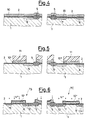
- FIGS. 1-6 show in succession the main steps of said process.
- FIG. 1 shows a P-type semiconductor substrate 1 covered by a layer of oxide 2 provided on the active areas 3 and 4 defined between field oxide zones 5.
- the area 3 is designed for formation of a selection transistor for an EEPROM cell while the area 4 is designed for formation of a high-voltage external circuitry transistor.
- a predetermined surface portion 6 of the substrate in the area of the selection transistor and two predetermined spaced surface portions 7 and 8 of said substrate are subjected to N ⁇ doping (e.g. phosphorous with doses between 1013 and 1014 atoms of phosphorous/cm3) using a resist mask 9 to protect the surface portions which are not to receive the dope.
- N ⁇ doping e.g. phosphorous with doses between 1013 and 1014 atoms of phosphorous/cm3
- the resist is then removed and the entire substrate surface is oxidized.
- the oxide grows more on the surface portions previously doped (FIG. 3).
- the following step calls for deposition of a layer of polysilicon 10 which is then N+ doped (FIG. 4).
- Another resist mask 11 subsequently allows definition of the polysilicon 10 in the form of two strips 10′ and 10 ⁇ of which the first is superimposed on a side part of the substrate surface portion 6 with N ⁇ doping and an adjacent undoped surface portion of said substrate and the second is superimposed on faced side parts of the substrate surface portions 7 and 8 with N ⁇ doping and on the interposed undoped surface portion of said substrate (FIG. 5).
- the two strips of polysilicon 10′ and 10 ⁇ are designed to form the gates of the two transistors being produced.
- N+ doping of the remaining parts 12, 13, 14, 15 of the substrate surface portions 6, 7, 8 and of another surface portion 15 located on the side of the gate 10′ opposite the surface portion 6 (FIG. 6).
- the surface portions 15 and 13 thus become the N+ source areas of the selection and external circuitry transistors respectively while the surface portions 12 and 14 become the N+ drain areas of said transistors, having respective portions 6 and 8 with N ⁇ doping under the gates 10′ and 10 ⁇ .
Landscapes
- Non-Volatile Memory (AREA)
- Metal-Oxide And Bipolar Metal-Oxide Semiconductor Integrated Circuits (AREA)
- Semiconductor Memories (AREA)
Claims (2)
- Verfahren zur gleichzeitigen Bildung einer Mehrzahl von N-Kanal-Transistoren für hohe Spannungen insbesondere für EEPROM-Speicher mit CMOS-Technologie, dadurch gekennzeichnet, daß es für jeden Transistor die nachfolgende Abfolge von Schritten umfaßt:(a) N⁻-Dotierung eines vorbestimmten Oberflächenbereichs (6, 8) eines P-leitenden Halbleitersubstrats (1), wobei das Substrat zuvor mit Gate-Oxid (2) bedeckt worden ist,(b) Oxidieren der Substratoberfläche,(c) Aufbringen und Definieren einer N⁺-dotieren Polysiliziumschicht (10) zur Bildung eines Polysilizium-Gate-Streifens (10′, 10˝) auf einem Seitenbereich des vorbestimmten Oberflächenbereichs (6, 8) sowie auf einem benachbarten Oberflächenbereich des Substrats,(d) Oxidieren des Polysilizium-Gate-Streifens (10′, 10˝), und(e) unter Verwendung des Polysilizium-Gate-Streifens als Maske erfolgende N⁺-Dotierung des übrigen Teils (12, 14) des vorbestimmten Oberflächenbereichs (6, 8) des Substrats zur Bildung eines Drain-Bereichs (12, 14), wobei der N⁻-dotierte Bereich (6, 8) unter dem Polysilizium-Gate-Streifen (10′, 10˝) liegt, sowie gleichzeitig eines weiteren Oberflächenbereichs (15, 13) des Substrats auf der entgegengesetzten Seite des Polysilizium-Gate-Streifens (10′, 10˝) zur Bildung eines Source-Bereichs (15, 13).
- Verfahren nach Anspruch 1,
dadurch gekennzeichnet, daß die N-Kanal-Transistoren für hohe Spannungen Auswähltransistoren und Transistoren für Schaltungseinrichtungen beinhalten und daß für jeden Auswähltransistor der Schritt (a) außerdem eine N⁻-Dotierung eines zusätzlichen Oberflächenbereichs (7) des Substrats beinhaltet, daß in Schritt (c) der Polysilizium-Gate-Streifen (10˝) auch auf einem Seitenbereich des zusätzlichen Oberflächenbereichs (7) ausgebildet wird, welcher dem Seitenbereich des vorbestimmten Oberflächenbereichs (8) gegenüberliegt, und daß in Schritt (e) der weitere Oberflächenbereich (13) der übrige Teil des zusätzlichen Oberflächenbereichs (7) ist.
Applications Claiming Priority (2)
| Application Number | Priority Date | Filing Date | Title |
|---|---|---|---|
| IT1958088 | 1988-02-29 | ||
| IT8819580A IT1216476B (it) | 1988-02-29 | 1988-02-29 | Processo per l'ottenimento di transitori a canale n per alta tensione, particolarmente per memorie eeprom con tecnologia cmos. |
Publications (3)
| Publication Number | Publication Date |
|---|---|
| EP0331223A2 EP0331223A2 (de) | 1989-09-06 |
| EP0331223A3 EP0331223A3 (de) | 1991-01-16 |
| EP0331223B1 true EP0331223B1 (de) | 1995-05-17 |
Family
ID=11159211
Family Applications (1)
| Application Number | Title | Priority Date | Filing Date |
|---|---|---|---|
| EP89200327A Expired - Lifetime EP0331223B1 (de) | 1988-02-29 | 1989-02-13 | Verfahren zur Herstellung eines N-Kanal-Transistors für Hochspannung, insbesondere für EEPROM-Speicher mit CMOS-Technologie |
Country Status (4)
| Country | Link |
|---|---|
| EP (1) | EP0331223B1 (de) |
| JP (1) | JP2554929B2 (de) |
| DE (1) | DE68922641T2 (de) |
| IT (1) | IT1216476B (de) |
Families Citing this family (2)
| Publication number | Priority date | Publication date | Assignee | Title |
|---|---|---|---|---|
| WO1995022174A1 (en) * | 1994-02-15 | 1995-08-17 | National Semiconductor Corporation | High-voltage cmos transistors for a standard cmos process |
| JP2007218716A (ja) * | 2006-02-16 | 2007-08-30 | Matsushita Electric Ind Co Ltd | 細胞電気生理センサ |
Family Cites Families (5)
| Publication number | Priority date | Publication date | Assignee | Title |
|---|---|---|---|---|
| JPS5947757A (ja) * | 1982-09-10 | 1984-03-17 | Hitachi Ltd | 半導体集積回路装置とその製造法 |
| KR910006249B1 (ko) * | 1983-04-01 | 1991-08-17 | 가부시기가이샤 히다찌세이사꾸쇼 | 반도체 장치 |
| US4577391A (en) * | 1984-07-27 | 1986-03-25 | Monolithic Memories, Inc. | Method of manufacturing CMOS devices |
| DE3583472D1 (de) * | 1984-08-28 | 1991-08-22 | Toshiba Kawasaki Kk | Verfahren zum herstellen einer halbleiteranordnung mit gateelektrode. |
| JPS61171165A (ja) * | 1985-01-25 | 1986-08-01 | Nissan Motor Co Ltd | Mosトランジスタ |
-
1988
- 1988-02-29 IT IT8819580A patent/IT1216476B/it active
-
1989
- 1989-02-13 EP EP89200327A patent/EP0331223B1/de not_active Expired - Lifetime
- 1989-02-13 DE DE68922641T patent/DE68922641T2/de not_active Expired - Fee Related
- 1989-02-22 JP JP1040447A patent/JP2554929B2/ja not_active Expired - Fee Related
Also Published As
| Publication number | Publication date |
|---|---|
| IT1216476B (it) | 1990-03-08 |
| EP0331223A2 (de) | 1989-09-06 |
| JPH027560A (ja) | 1990-01-11 |
| EP0331223A3 (de) | 1991-01-16 |
| DE68922641T2 (de) | 1996-02-08 |
| JP2554929B2 (ja) | 1996-11-20 |
| IT8819580A0 (it) | 1988-02-29 |
| DE68922641D1 (de) | 1995-06-22 |
Similar Documents
| Publication | Publication Date | Title |
|---|---|---|
| US4342149A (en) | Method of making very short channel length MNOS and MOS devices by double implantation of one conductivity type subsequent to other type implantation | |
| US4487639A (en) | Localized epitaxy for VLSI devices | |
| KR100230610B1 (ko) | 자기정렬된 웰탭을 지니는 bicmos 디바이스 및 그 제조방법 | |
| US4637124A (en) | Process for fabricating semiconductor integrated circuit device | |
| US4849364A (en) | Semiconductor devices | |
| JPH02237160A (ja) | 半導体装置 | |
| EP0465045B1 (de) | Verfahren zum Herstellen von Feldeffekt-Transistoren für integrierte Schaltungen | |
| JPS63239856A (ja) | 半導体集積回路装置及びその製造方法 | |
| US5304501A (en) | BiCMOS process with low base recombination current bipolar transistors | |
| EP0187260B1 (de) | Verfahren zur Herstellung einer integrierten Halbleiterschaltungsanordnung, die MISFETs enthält | |
| JPH05326552A (ja) | 半導体素子およびその製造方法 | |
| US5086008A (en) | Process for obtaining high-voltage N channel transistors particularly for EEPROM memories with CMOS technology | |
| US5998266A (en) | Method of forming a semiconductor structure having laterally merged body layer | |
| EP0331223B1 (de) | Verfahren zur Herstellung eines N-Kanal-Transistors für Hochspannung, insbesondere für EEPROM-Speicher mit CMOS-Technologie | |
| US5518938A (en) | Process for fabricating a CMOS transistor having high-voltage metal-gate | |
| US5411900A (en) | Method of fabricating a monolithic integrated circuit with at least one CMOS field-effect transistor and one NPN bipolar transistor | |
| KR950021503A (ko) | 병합 디바이스를 지원하기 위한 바이씨모스(BiCMOS) 및 이의 형성방법 | |
| US5525825A (en) | Monolithic integrated circuit with at least one CMOS field-effect transistor and one npn bipolar transistor | |
| JP3190370B2 (ja) | 密接して離隔したコンタクトを有するBiCMOS装置及びその製造方法 | |
| US5597757A (en) | Method of manufacturing a semiconductor device including bipolar and MOS transistors | |
| JPS62265765A (ja) | 半導体装置の製造方法 | |
| JPH0612826B2 (ja) | 薄膜トランジスタの製造方法 | |
| JPH03225963A (ja) | 高耐圧misトランジスタ | |
| TW447132B (en) | Method to fabricate MOSFET | |
| JPH0669439A (ja) | Cmos半導体装置の製造方法 |
Legal Events
| Date | Code | Title | Description |
|---|---|---|---|
| PUAI | Public reference made under article 153(3) epc to a published international application that has entered the european phase |
Free format text: ORIGINAL CODE: 0009012 |
|
| AK | Designated contracting states |
Kind code of ref document: A2 Designated state(s): DE FR GB NL SE |
|
| PUAL | Search report despatched |
Free format text: ORIGINAL CODE: 0009013 |
|
| AK | Designated contracting states |
Kind code of ref document: A3 Designated state(s): DE FR GB NL SE |
|
| 17P | Request for examination filed |
Effective date: 19910520 |
|
| 17Q | First examination report despatched |
Effective date: 19930917 |
|
| GRAA | (expected) grant |
Free format text: ORIGINAL CODE: 0009210 |
|
| AK | Designated contracting states |
Kind code of ref document: B1 Designated state(s): DE FR GB NL SE |
|
| PG25 | Lapsed in a contracting state [announced via postgrant information from national office to epo] |
Ref country code: NL Free format text: LAPSE BECAUSE OF FAILURE TO SUBMIT A TRANSLATION OF THE DESCRIPTION OR TO PAY THE FEE WITHIN THE PRESCRIBED TIME-LIMIT Effective date: 19950517 |
|
| REF | Corresponds to: |
Ref document number: 68922641 Country of ref document: DE Date of ref document: 19950622 |
|
| ET | Fr: translation filed | ||
| PG25 | Lapsed in a contracting state [announced via postgrant information from national office to epo] |
Ref country code: SE Effective date: 19950817 |
|
| NLV1 | Nl: lapsed or annulled due to failure to fulfill the requirements of art. 29p and 29m of the patents act | ||
| PLBE | No opposition filed within time limit |
Free format text: ORIGINAL CODE: 0009261 |
|
| STAA | Information on the status of an ep patent application or granted ep patent |
Free format text: STATUS: NO OPPOSITION FILED WITHIN TIME LIMIT |
|
| 26N | No opposition filed | ||
| REG | Reference to a national code |
Ref country code: FR Ref legal event code: D6 |
|
| REG | Reference to a national code |
Ref country code: GB Ref legal event code: IF02 |
|
| PGFP | Annual fee paid to national office [announced via postgrant information from national office to epo] |
Ref country code: GB Payment date: 20020802 Year of fee payment: 14 |
|
| PGFP | Annual fee paid to national office [announced via postgrant information from national office to epo] |
Ref country code: DE Payment date: 20020827 Year of fee payment: 14 |
|
| PGFP | Annual fee paid to national office [announced via postgrant information from national office to epo] |
Ref country code: FR Payment date: 20020828 Year of fee payment: 14 |
|
| PG25 | Lapsed in a contracting state [announced via postgrant information from national office to epo] |
Ref country code: GB Free format text: LAPSE BECAUSE OF NON-PAYMENT OF DUE FEES Effective date: 20030213 |
|
| PG25 | Lapsed in a contracting state [announced via postgrant information from national office to epo] |
Ref country code: DE Free format text: LAPSE BECAUSE OF NON-PAYMENT OF DUE FEES Effective date: 20030902 |
|
| GBPC | Gb: european patent ceased through non-payment of renewal fee | ||
| PG25 | Lapsed in a contracting state [announced via postgrant information from national office to epo] |
Ref country code: FR Free format text: LAPSE BECAUSE OF NON-PAYMENT OF DUE FEES Effective date: 20031031 |
|
| REG | Reference to a national code |
Ref country code: FR Ref legal event code: ST |