EP0331223A2 - Verfahren zur Herstellung eines N-Kanal-Transistors für Hochspannung, insbesondere für EEPROM-Speicher mit CMOS-Technologie - Google Patents
Verfahren zur Herstellung eines N-Kanal-Transistors für Hochspannung, insbesondere für EEPROM-Speicher mit CMOS-Technologie Download PDFInfo
- Publication number
- EP0331223A2 EP0331223A2 EP89200327A EP89200327A EP0331223A2 EP 0331223 A2 EP0331223 A2 EP 0331223A2 EP 89200327 A EP89200327 A EP 89200327A EP 89200327 A EP89200327 A EP 89200327A EP 0331223 A2 EP0331223 A2 EP 0331223A2
- Authority
- EP
- European Patent Office
- Prior art keywords
- doping
- substrate
- voltage
- gate
- area
- Prior art date
- Legal status (The legal status is an assumption and is not a legal conclusion. Google has not performed a legal analysis and makes no representation as to the accuracy of the status listed.)
- Granted
Links
Images

Classifications
-
- H—ELECTRICITY
- H10—SEMICONDUCTOR DEVICES; ELECTRIC SOLID-STATE DEVICES NOT OTHERWISE PROVIDED FOR
- H10D—INORGANIC ELECTRIC SEMICONDUCTOR DEVICES
- H10D30/00—Field-effect transistors [FET]
- H10D30/01—Manufacture or treatment
- H10D30/021—Manufacture or treatment of FETs having insulated gates [IGFET]
- H10D30/0221—Manufacture or treatment of FETs having insulated gates [IGFET] having asymmetry in the channel direction, e.g. lateral high-voltage MISFETs having drain offset region or extended-drain MOSFETs [EDMOS]
-
- H—ELECTRICITY
- H10—SEMICONDUCTOR DEVICES; ELECTRIC SOLID-STATE DEVICES NOT OTHERWISE PROVIDED FOR
- H10D—INORGANIC ELECTRIC SEMICONDUCTOR DEVICES
- H10D30/00—Field-effect transistors [FET]
- H10D30/60—Insulated-gate field-effect transistors [IGFET]
-
- H—ELECTRICITY
- H10—SEMICONDUCTOR DEVICES; ELECTRIC SOLID-STATE DEVICES NOT OTHERWISE PROVIDED FOR
- H10D—INORGANIC ELECTRIC SEMICONDUCTOR DEVICES
- H10D84/00—Integrated devices formed in or on semiconductor substrates that comprise only semiconducting layers, e.g. on Si wafers or on GaAs-on-Si wafers
- H10D84/01—Manufacture or treatment
- H10D84/0123—Integrating together multiple components covered by H10D12/00 or H10D30/00, e.g. integrating multiple IGBTs
- H10D84/0126—Integrating together multiple components covered by H10D12/00 or H10D30/00, e.g. integrating multiple IGBTs the components including insulated gates, e.g. IGFETs
- H10D84/0165—Integrating together multiple components covered by H10D12/00 or H10D30/00, e.g. integrating multiple IGBTs the components including insulated gates, e.g. IGFETs the components including complementary IGFETs, e.g. CMOS devices
-
- H—ELECTRICITY
- H10—SEMICONDUCTOR DEVICES; ELECTRIC SOLID-STATE DEVICES NOT OTHERWISE PROVIDED FOR
- H10D—INORGANIC ELECTRIC SEMICONDUCTOR DEVICES
- H10D84/00—Integrated devices formed in or on semiconductor substrates that comprise only semiconducting layers, e.g. on Si wafers or on GaAs-on-Si wafers
- H10D84/01—Manufacture or treatment
- H10D84/02—Manufacture or treatment characterised by using material-based technologies
- H10D84/03—Manufacture or treatment characterised by using material-based technologies using Group IV technology, e.g. silicon technology or silicon-carbide [SiC] technology
- H10D84/038—Manufacture or treatment characterised by using material-based technologies using Group IV technology, e.g. silicon technology or silicon-carbide [SiC] technology using silicon technology, e.g. SiGe
-
- H—ELECTRICITY
- H10—SEMICONDUCTOR DEVICES; ELECTRIC SOLID-STATE DEVICES NOT OTHERWISE PROVIDED FOR
- H10D—INORGANIC ELECTRIC SEMICONDUCTOR DEVICES
- H10D84/00—Integrated devices formed in or on semiconductor substrates that comprise only semiconducting layers, e.g. on Si wafers or on GaAs-on-Si wafers
- H10D84/80—Integrated devices formed in or on semiconductor substrates that comprise only semiconducting layers, e.g. on Si wafers or on GaAs-on-Si wafers characterised by the integration of at least one component covered by groups H10D12/00 or H10D30/00, e.g. integration of IGFETs
- H10D84/82—Integrated devices formed in or on semiconductor substrates that comprise only semiconducting layers, e.g. on Si wafers or on GaAs-on-Si wafers characterised by the integration of at least one component covered by groups H10D12/00 or H10D30/00, e.g. integration of IGFETs of only field-effect components
- H10D84/83—Integrated devices formed in or on semiconductor substrates that comprise only semiconducting layers, e.g. on Si wafers or on GaAs-on-Si wafers characterised by the integration of at least one component covered by groups H10D12/00 or H10D30/00, e.g. integration of IGFETs of only field-effect components of only insulated-gate FETs [IGFET]
- H10D84/8312—Integrated devices formed in or on semiconductor substrates that comprise only semiconducting layers, e.g. on Si wafers or on GaAs-on-Si wafers characterised by the integration of at least one component covered by groups H10D12/00 or H10D30/00, e.g. integration of IGFETs of only field-effect components of only insulated-gate FETs [IGFET] the IGFETs characterised by having different source or drain region structures, e.g. IGFETs having symmetrical source or drain regions integrated with IGFETs having asymmetrical source or drain regions
-
- H—ELECTRICITY
- H10—SEMICONDUCTOR DEVICES; ELECTRIC SOLID-STATE DEVICES NOT OTHERWISE PROVIDED FOR
- H10D—INORGANIC ELECTRIC SEMICONDUCTOR DEVICES
- H10D30/00—Field-effect transistors [FET]
- H10D30/60—Insulated-gate field-effect transistors [IGFET]
- H10D30/601—Insulated-gate field-effect transistors [IGFET] having lightly-doped drain or source extensions, e.g. LDD IGFETs or DDD IGFETs
- H10D30/603—Insulated-gate field-effect transistors [IGFET] having lightly-doped drain or source extensions, e.g. LDD IGFETs or DDD IGFETs having asymmetry in the channel direction, e.g. lateral high-voltage MISFETs having drain offset region or extended drain IGFETs [EDMOS]
-
- H—ELECTRICITY
- H10—SEMICONDUCTOR DEVICES; ELECTRIC SOLID-STATE DEVICES NOT OTHERWISE PROVIDED FOR
- H10D—INORGANIC ELECTRIC SEMICONDUCTOR DEVICES
- H10D30/00—Field-effect transistors [FET]
- H10D30/60—Insulated-gate field-effect transistors [IGFET]
- H10D30/601—Insulated-gate field-effect transistors [IGFET] having lightly-doped drain or source extensions, e.g. LDD IGFETs or DDD IGFETs
- H10D30/605—Insulated-gate field-effect transistors [IGFET] having lightly-doped drain or source extensions, e.g. LDD IGFETs or DDD IGFETs having significant overlap between the lightly-doped extensions and the gate electrode
-
- H—ELECTRICITY
- H10—SEMICONDUCTOR DEVICES; ELECTRIC SOLID-STATE DEVICES NOT OTHERWISE PROVIDED FOR
- H10D—INORGANIC ELECTRIC SEMICONDUCTOR DEVICES
- H10D84/00—Integrated devices formed in or on semiconductor substrates that comprise only semiconducting layers, e.g. on Si wafers or on GaAs-on-Si wafers
- H10D84/80—Integrated devices formed in or on semiconductor substrates that comprise only semiconducting layers, e.g. on Si wafers or on GaAs-on-Si wafers characterised by the integration of at least one component covered by groups H10D12/00 or H10D30/00, e.g. integration of IGFETs
- H10D84/82—Integrated devices formed in or on semiconductor substrates that comprise only semiconducting layers, e.g. on Si wafers or on GaAs-on-Si wafers characterised by the integration of at least one component covered by groups H10D12/00 or H10D30/00, e.g. integration of IGFETs of only field-effect components
- H10D84/83—Integrated devices formed in or on semiconductor substrates that comprise only semiconducting layers, e.g. on Si wafers or on GaAs-on-Si wafers characterised by the integration of at least one component covered by groups H10D12/00 or H10D30/00, e.g. integration of IGFETs of only field-effect components of only insulated-gate FETs [IGFET]
- H10D84/8311—Integrated devices formed in or on semiconductor substrates that comprise only semiconducting layers, e.g. on Si wafers or on GaAs-on-Si wafers characterised by the integration of at least one component covered by groups H10D12/00 or H10D30/00, e.g. integration of IGFETs of only field-effect components of only insulated-gate FETs [IGFET] the IGFETs characterised by having different channel structures
Definitions
- the present invention relates to a process for obtaining high-voltage N channel transistors particularly for EEPROM memories with CMOS technology.
- N channel transistors are known and can be found in the literature
- One of these which is used particularly for selection and external circuitry transistors in EEPROM memories with CMOS technology calls for in succession deposit and definition of a layer of polysilicon on a semiconductor substrate covered with gate oxide for the formation of a gate area, N+ doping of a first predetermined portion of the substrate on one side of said gate area for the formation of a source area and of a second predetermined portion of the substrate on the other side of said gate area and spaced therefrom for the formation of a drain area and finally the N ⁇ doping of an intermediate portion of the substrate between said gate area and said drain area for the formation of an extension of the drain area with lower N doping.
- the drain junction near the gate has low-concentration doping which permits limiting the electric field in that zone between gate and diffusion and consequently amplification of the working voltage field which the transistor is able to accept without breaking the gate oxide between the drain and the gate.
- the object of the present invention is to accomplish a process for obtaining high voltage N channel transistors which would be usable in place of the known process mentioned above to obtain the N channel transistors of an EEPROM memory with CMOS technology while the P channel transistors of said memory are still obtained by the known process without requiring the use of additional masks.
- said object is achieved by a process for obtaining high-voltage N channel transistors characterized in that it comprises in succession the steps (a) the N ⁇ doping of at least one predetermined portion of a type-P semiconductor substrate covered with gate oxide, (b) deposit and definition of an appropriately N+ doped polysilicon layer on a part of said predetermined portion and on an adjacent portion of the substrate for formation of a gate area, (c) oxidation of the polysicon and (d) N+ doping of the remaining part of said predetermined portion of the substrate for formation of a drain area partly N doped under the gate area and another portion of the substrate on the side opposite said gate area for formation of a source area.
- this process may be used for high-voltage N channel transistors while the known process continues to be used for the P channel transistors with no requirement for additional masks.
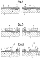
- FIGS. 1-6 show in succession the main steps of said process.
- FIG. 1 shows a P-type semiconductor substrate 1 covered by a layer of oxide 2 provided on the active areas 3 and 4 defined between field oxide zones 5.
- the area 3 is designed for formation of a selection transistor for an EEPROM cell while the area 4 is designed for formation of a high-voltage external circuitry transistor.
- a predetermined portion 6 of the substrate in the area of the selection transistor and two predetermined spaced portions 7 and 8 of said substrate are subjected to N ⁇ doping (e.g. phosphorous with doses between 1013 and 1014 atoms of phosphorous/cm3) using a resist mask 9 to protect the portions which are not to receive the dope.
- N ⁇ doping e.g. phosphorous with doses between 1013 and 1014 atoms of phosphorous/cm3
- the resist is then removed and the entire surface is oxidized. In a known manner the oxide grows more on the portions previously doped (FIG. 3).
- the following step calls for deposit of a layer of polysilicon 10 which is then N+ doped (FIG. 4).
- Another resist mask 11 subsequently allows definition of the polysilicon 10 in the form of two strips 10′ and 10 ⁇ of which the first is superimposed on a part of the portion of substrate 6 with N ⁇ doping and an adjacent undoped portion of said substrate and the second is superimposed on a part of each portion of substrate 7 and 8 with N ⁇ doping and on the interposed undoped portion of said substrate (FIG. 5).
- the two strips of polysilicon 10′ and 10 ⁇ are designed to form the gates of the two transistors being produced.
- the portions 15 and 13 thus become the N+ source areas of the selection and external circuitry transistors respectively while the portions 12 and 14 become the N+ drain areas of said transistors, having respective portions with N ⁇ doping 6 and 8 under the gates 10′ and 10 ⁇ .
Landscapes
- Non-Volatile Memory (AREA)
- Metal-Oxide And Bipolar Metal-Oxide Semiconductor Integrated Circuits (AREA)
- Semiconductor Memories (AREA)
Applications Claiming Priority (2)
| Application Number | Priority Date | Filing Date | Title |
|---|---|---|---|
| IT8819580A IT1216476B (it) | 1988-02-29 | 1988-02-29 | Processo per l'ottenimento di transitori a canale n per alta tensione, particolarmente per memorie eeprom con tecnologia cmos. |
| IT1958088 | 1988-02-29 |
Publications (3)
| Publication Number | Publication Date |
|---|---|
| EP0331223A2 true EP0331223A2 (de) | 1989-09-06 |
| EP0331223A3 EP0331223A3 (de) | 1991-01-16 |
| EP0331223B1 EP0331223B1 (de) | 1995-05-17 |
Family
ID=11159211
Family Applications (1)
| Application Number | Title | Priority Date | Filing Date |
|---|---|---|---|
| EP89200327A Expired - Lifetime EP0331223B1 (de) | 1988-02-29 | 1989-02-13 | Verfahren zur Herstellung eines N-Kanal-Transistors für Hochspannung, insbesondere für EEPROM-Speicher mit CMOS-Technologie |
Country Status (4)
| Country | Link |
|---|---|
| EP (1) | EP0331223B1 (de) |
| JP (1) | JP2554929B2 (de) |
| DE (1) | DE68922641T2 (de) |
| IT (1) | IT1216476B (de) |
Cited By (1)
| Publication number | Priority date | Publication date | Assignee | Title |
|---|---|---|---|---|
| WO1995022174A1 (en) * | 1994-02-15 | 1995-08-17 | National Semiconductor Corporation | High-voltage cmos transistors for a standard cmos process |
Families Citing this family (1)
| Publication number | Priority date | Publication date | Assignee | Title |
|---|---|---|---|---|
| JP2007218716A (ja) * | 2006-02-16 | 2007-08-30 | Matsushita Electric Ind Co Ltd | 細胞電気生理センサ |
Family Cites Families (5)
| Publication number | Priority date | Publication date | Assignee | Title |
|---|---|---|---|---|
| JPS5947757A (ja) * | 1982-09-10 | 1984-03-17 | Hitachi Ltd | 半導体集積回路装置とその製造法 |
| KR910006249B1 (ko) * | 1983-04-01 | 1991-08-17 | 가부시기가이샤 히다찌세이사꾸쇼 | 반도체 장치 |
| US4577391A (en) * | 1984-07-27 | 1986-03-25 | Monolithic Memories, Inc. | Method of manufacturing CMOS devices |
| US4642878A (en) * | 1984-08-28 | 1987-02-17 | Kabushiki Kaisha Toshiba | Method of making MOS device by sequentially depositing an oxidizable layer and a masking second layer over gated device regions |
| JPS61171165A (ja) * | 1985-01-25 | 1986-08-01 | Nissan Motor Co Ltd | Mosトランジスタ |
-
1988
- 1988-02-29 IT IT8819580A patent/IT1216476B/it active
-
1989
- 1989-02-13 DE DE68922641T patent/DE68922641T2/de not_active Expired - Fee Related
- 1989-02-13 EP EP89200327A patent/EP0331223B1/de not_active Expired - Lifetime
- 1989-02-22 JP JP1040447A patent/JP2554929B2/ja not_active Expired - Fee Related
Cited By (1)
| Publication number | Priority date | Publication date | Assignee | Title |
|---|---|---|---|---|
| WO1995022174A1 (en) * | 1994-02-15 | 1995-08-17 | National Semiconductor Corporation | High-voltage cmos transistors for a standard cmos process |
Also Published As
| Publication number | Publication date |
|---|---|
| EP0331223A3 (de) | 1991-01-16 |
| EP0331223B1 (de) | 1995-05-17 |
| IT8819580A0 (it) | 1988-02-29 |
| DE68922641D1 (de) | 1995-06-22 |
| IT1216476B (it) | 1990-03-08 |
| JP2554929B2 (ja) | 1996-11-20 |
| JPH027560A (ja) | 1990-01-11 |
| DE68922641T2 (de) | 1996-02-08 |
Similar Documents
| Publication | Publication Date | Title |
|---|---|---|
| US4342149A (en) | Method of making very short channel length MNOS and MOS devices by double implantation of one conductivity type subsequent to other type implantation | |
| US5013678A (en) | Method of making an integrated circuit comprising load resistors arranged on the field oxide zones which separate the active transistor zones | |
| US5663080A (en) | Process for manufacturing MOS-type integrated circuits | |
| US4550490A (en) | Monolithic integrated circuit | |
| US6025219A (en) | Method of manufacturing a semiconductor device having MOS transistor and bipolar transistor in mixture on the same substrate | |
| US5086008A (en) | Process for obtaining high-voltage N channel transistors particularly for EEPROM memories with CMOS technology | |
| US5489545A (en) | Method of manufacturing an integrated circuit having a charge coupled device and a MOS transistor | |
| EP0331223A2 (de) | Verfahren zur Herstellung eines N-Kanal-Transistors für Hochspannung, insbesondere für EEPROM-Speicher mit CMOS-Technologie | |
| US5518938A (en) | Process for fabricating a CMOS transistor having high-voltage metal-gate | |
| US5411900A (en) | Method of fabricating a monolithic integrated circuit with at least one CMOS field-effect transistor and one NPN bipolar transistor | |
| US5759881A (en) | Low cost well process | |
| US4833097A (en) | Fabrication of MOS-transistors | |
| JPS62265765A (ja) | 半導体装置の製造方法 | |
| JPH0669439A (ja) | Cmos半導体装置の製造方法 | |
| JPH05335503A (ja) | 半導体装置の製造方法 | |
| JP4146374B2 (ja) | 半導体装置の製造方法 | |
| JPH1131814A (ja) | 半導体装置の製造方法 | |
| JPH11150181A (ja) | 半導体装置の製造方法 | |
| JP2000188262A (ja) | 半導体装置のウェル形成方法 | |
| JPH04369261A (ja) | 半導体装置の製造方法 | |
| JPH0423358A (ja) | 半導体装置の製造方法 | |
| JPH03181136A (ja) | 半導体装置の製造方法 | |
| JPH10163490A (ja) | トランジスタの製造方法 | |
| JPH0387058A (ja) | 半導体集積回路の製造方法 | |
| JPS634668A (ja) | Mos型半導体装置 |
Legal Events
| Date | Code | Title | Description |
|---|---|---|---|
| PUAI | Public reference made under article 153(3) epc to a published international application that has entered the european phase |
Free format text: ORIGINAL CODE: 0009012 |
|
| AK | Designated contracting states |
Kind code of ref document: A2 Designated state(s): DE FR GB NL SE |
|
| PUAL | Search report despatched |
Free format text: ORIGINAL CODE: 0009013 |
|
| AK | Designated contracting states |
Kind code of ref document: A3 Designated state(s): DE FR GB NL SE |
|
| 17P | Request for examination filed |
Effective date: 19910520 |
|
| 17Q | First examination report despatched |
Effective date: 19930917 |
|
| GRAA | (expected) grant |
Free format text: ORIGINAL CODE: 0009210 |
|
| AK | Designated contracting states |
Kind code of ref document: B1 Designated state(s): DE FR GB NL SE |
|
| PG25 | Lapsed in a contracting state [announced via postgrant information from national office to epo] |
Ref country code: NL Free format text: LAPSE BECAUSE OF FAILURE TO SUBMIT A TRANSLATION OF THE DESCRIPTION OR TO PAY THE FEE WITHIN THE PRESCRIBED TIME-LIMIT Effective date: 19950517 |
|
| REF | Corresponds to: |
Ref document number: 68922641 Country of ref document: DE Date of ref document: 19950622 |
|
| ET | Fr: translation filed | ||
| PG25 | Lapsed in a contracting state [announced via postgrant information from national office to epo] |
Ref country code: SE Effective date: 19950817 |
|
| NLV1 | Nl: lapsed or annulled due to failure to fulfill the requirements of art. 29p and 29m of the patents act | ||
| PLBE | No opposition filed within time limit |
Free format text: ORIGINAL CODE: 0009261 |
|
| STAA | Information on the status of an ep patent application or granted ep patent |
Free format text: STATUS: NO OPPOSITION FILED WITHIN TIME LIMIT |
|
| 26N | No opposition filed | ||
| REG | Reference to a national code |
Ref country code: FR Ref legal event code: D6 |
|
| REG | Reference to a national code |
Ref country code: GB Ref legal event code: IF02 |
|
| PGFP | Annual fee paid to national office [announced via postgrant information from national office to epo] |
Ref country code: GB Payment date: 20020802 Year of fee payment: 14 |
|
| PGFP | Annual fee paid to national office [announced via postgrant information from national office to epo] |
Ref country code: DE Payment date: 20020827 Year of fee payment: 14 |
|
| PGFP | Annual fee paid to national office [announced via postgrant information from national office to epo] |
Ref country code: FR Payment date: 20020828 Year of fee payment: 14 |
|
| PG25 | Lapsed in a contracting state [announced via postgrant information from national office to epo] |
Ref country code: GB Free format text: LAPSE BECAUSE OF NON-PAYMENT OF DUE FEES Effective date: 20030213 |
|
| PG25 | Lapsed in a contracting state [announced via postgrant information from national office to epo] |
Ref country code: DE Free format text: LAPSE BECAUSE OF NON-PAYMENT OF DUE FEES Effective date: 20030902 |
|
| GBPC | Gb: european patent ceased through non-payment of renewal fee | ||
| PG25 | Lapsed in a contracting state [announced via postgrant information from national office to epo] |
Ref country code: FR Free format text: LAPSE BECAUSE OF NON-PAYMENT OF DUE FEES Effective date: 20031031 |
|
| REG | Reference to a national code |
Ref country code: FR Ref legal event code: ST |