EP0332274B1 - EEPROM à mode d'effacement et d'écriture commandé par des données - Google Patents
EEPROM à mode d'effacement et d'écriture commandé par des données Download PDFInfo
- Publication number
- EP0332274B1 EP0332274B1 EP89200552A EP89200552A EP0332274B1 EP 0332274 B1 EP0332274 B1 EP 0332274B1 EP 89200552 A EP89200552 A EP 89200552A EP 89200552 A EP89200552 A EP 89200552A EP 0332274 B1 EP0332274 B1 EP 0332274B1
- Authority
- EP
- European Patent Office
- Prior art keywords
- transistor
- coupled
- control
- transistors
- node
- Prior art date
- Legal status (The legal status is an assumption and is not a legal conclusion. Google has not performed a legal analysis and makes no representation as to the accuracy of the status listed.)
- Expired - Lifetime
Links
Images


Classifications
-
- G—PHYSICS
- G11—INFORMATION STORAGE
- G11C—STATIC STORES
- G11C11/00—Digital stores characterised by the use of particular electric or magnetic storage elements; Storage elements therefor
- G11C11/21—Digital stores characterised by the use of particular electric or magnetic storage elements; Storage elements therefor using electric elements
- G11C11/34—Digital stores characterised by the use of particular electric or magnetic storage elements; Storage elements therefor using electric elements using semiconductor devices
- G11C11/40—Digital stores characterised by the use of particular electric or magnetic storage elements; Storage elements therefor using electric elements using semiconductor devices using transistors
-
- G—PHYSICS
- G11—INFORMATION STORAGE
- G11C—STATIC STORES
- G11C16/00—Erasable programmable read-only memories
- G11C16/02—Erasable programmable read-only memories electrically programmable
- G11C16/06—Auxiliary circuits, e.g. for writing into memory
- G11C16/30—Power supply circuits
-
- G—PHYSICS
- G11—INFORMATION STORAGE
- G11C—STATIC STORES
- G11C16/00—Erasable programmable read-only memories
- G11C16/02—Erasable programmable read-only memories electrically programmable
- G11C16/06—Auxiliary circuits, e.g. for writing into memory
- G11C16/10—Programming or data input circuits
-
- G—PHYSICS
- G11—INFORMATION STORAGE
- G11C—STATIC STORES
- G11C16/00—Erasable programmable read-only memories
- G11C16/02—Erasable programmable read-only memories electrically programmable
- G11C16/06—Auxiliary circuits, e.g. for writing into memory
- G11C16/10—Programming or data input circuits
- G11C16/14—Circuits for erasing electrically, e.g. erase voltage switching circuits
-
- G—PHYSICS
- G11—INFORMATION STORAGE
- G11C—STATIC STORES
- G11C2216/00—Indexing scheme relating to G11C16/00 and subgroups, for features not directly covered by these groups
- G11C2216/12—Reading and writing aspects of erasable programmable read-only memories
- G11C2216/22—Nonvolatile memory in which reading can be carried out from one memory bank or array whilst a word or sector in another bank or array is being erased or programmed simultaneously
-
- G—PHYSICS
- G11—INFORMATION STORAGE
- G11C—STATIC STORES
- G11C2216/00—Indexing scheme relating to G11C16/00 and subgroups, for features not directly covered by these groups
- G11C2216/12—Reading and writing aspects of erasable programmable read-only memories
- G11C2216/24—Nonvolatile memory in which programming can be carried out in one memory bank or array whilst a word or sector in another bank or array is being erased simultaneously
Definitions
- the invention relates to an integrated memory circuit comprising an EEROM having a data controlled erasing and writing mode
- EP-A-0 131 344 discloses an integrated circuit with a byte organized EEPROM.
- the EEPROM has a plurality of memory cells arranged in rows and columns. The columns are organized in a plurality of sections. The bit cells associated with a single byte are distributed over the sections such that a respective bit cell of the byte is located in a column of a respective section. Each section individually has a writing circuit.
- the writing circuits can be activated independently form one another depending on whether or not the cell to be written stores the same logic level as of the bit signal that one intends to write into the cell.
- EP-A-0 131 344 discloses all the features of the preamble of claim 1.
- a memory circuit is known from the international PCT-publication WO 83/01148.
- a plurality of columns is coupled to the memory data input via column selection gates.
- Each memory location comprises a plurality of bit cells.
- Each bit cell is connected between a bit line and a voltage terminal and comprises a series arrangement of a conduction channel of a selection transistor and a conduction channel of a programmable transistor having a floating gate.
- the voltage terminal is common to all bit cells in the memory and serves to feed a first supply voltage to each bit cell in an erase mode of the memory and to feed a second supply voltage to each bit cell in a program mode of the memory.
- In the program mode one memory location at a time can be programmed because of the single memory data input that has to be switched towards the selected column.
- the memory is able to operate in several erase modes: a single-memory-location erase mode, a row erase mode, a column erase mode and erase modes for erasing the whole memory matrix or a submatrix. Because of the global connection of the memory to said voltage terminal the erasure of a particular memory location and the programming of another particular memory location need to be separated in time and therefore need to be controlled by control circuitry outputting control signals in order to distinguish between a program mode or an erase mode.
- a memory circuit In a memory circuit according to the invention as set forth in claim 1 only the data presented determines whether the selected memory location is to be erased or to be programmed.
- Each column has its own programming circuit controlled by the data fed to the respective data input, only the data discriminate between an erasure and a programming of a selected memory location.
- the programming means of a plurality of columns are addressable simultaneously by respective data simultaneously fed to the respective data inputs and simultaneous erasure and programming are allowed for various memory sections of a same row under data control.
- latch means in each programming circuit respective data are allowed to enter the memory circuit sequentially to be temporarily stored in the respective latches. After a full row of latches has received the data, the memory sections of a same row are activated in parallel, some of said sections undergoing an erasure others a programming, depending on the particular data.
- the detector gate means comprises a logic gate means having a gate input coupled to said data input and having a gate output coupled to a further latch means.
- FIG. 1 there is shown by way of example a memory circuit according to the invention.
- Memory locations 10, 20, 30 and 40 form part of a memory matrix, which has not further been drawn for clarity, locations 10 and 20 being situated at a same row, locations 10 and 30 being situated at a same column. Only memory location 10 has been drawn in further detail for clarity.
- Each memory location comprises a plurality of bit cells 10a, ... 10b, each bit cell comprising a programmable transistor 11a, 11b having a floating gate and a selection transistor 12a, 12b, the conduction channels thereof being disposed in a series arrangement between a supply line 13a, 13b and a bit line 14a, 14b.
- Corresponding bit cells in the memory location 30 are connected in the same way to the corresponding bit-line-suppy-line-pair.
- Each bit cell 10a, 10b has two logic states. A first logic state which is denoted by a "1" and is represented by a charged floating gate. A second logic state is denoted by a "0" and is represented by a non-charged floating gate. Only the first logic state is actively programmed by forcing a tunnel current from the floating gate to the junction point of the selection transistor and the programmable transistor during a write cycle. This causes a charge at the floating gate and hence an enduring increase of the absolute value of the programmable transistor's threshold voltage. The bit cell is erased by forcing a tunnel current into the opposite direction.
- control electrodes of the selection transistors 12a, 12b are connected to word line 15, that is common to the selection transistors of the memory locations disposed in the same row.
- the programmable transistors 11a, 11b of memory location 10 have their control electrodes connected to an activation line 16. Each individual memory location has been provided with such an activation line.
- the function of the supply lines 13a, 13b, bit lines 14a, 14b, activation line 16 and word line 15 with regard to the programming or erasure of memory location 10 will be described hereinafter.
- memory location 10 comprises a switch 17, having a first switch transistor 17a connected to the supply voltage and a second switch transistor 17b, a conduction channel thereof being disposed between word line 15 and activation line 16. Each memory location has been provided with an individual switch.
- the second voltage generating means 50 controls switch 17, together with other switches of the memory locations located in the same column.
- the suppy lines 13a, 13b and bit lines 14a, 14b are controlled by the first voltage generating means 60.
- Each individual column has been provided with associated first voltage generating means 60, 80, and with second voltage generating means 50, 70.
- the depicted transistors are supposed to be of the PMOS-field-effect type.
- word line 15 has to be charged to a negative high voltage V EE
- activation line 16 has to be charged to a supply voltage V DD
- supply line 13a has to be floating for avoiding the occurrence of detrimentally high electrical fields in the programmable transistor 11a
- bit line 14a has to be charged to the negative high voltage V EE .
- supply lines 13a, 13b and bit lines 14a, 14b have to be charged to supply voltage V DD
- activation line 16 and word line 15 have to be charged to the negative high voltage V EE .
- the logical contents of an already erased bit cell 10a is maintained if supply line 13a and bit line 14a are kept at the supply voltage V DD while word line 15 and activation line 16 carry the negative high voltage V EE .
- the operation of the first voltage generating means 60 and the second voltage generating means 50 will now be described.
- an erasure of a selected memory location occurs in case the data at the memory data input has a predetermined logic value, that is, in case the data presented at the first data input, that comprises terminals 61a, 61b, have a predetermined bit combination.
- the second voltage generating means comprises a NOR-gate 51.
- bit cells 10a, 10b of memory location 10 have a logic "0" as logic content.
- a logic "1” is presented at terminal 61a and a logic "0” is presented at terminal 61b to be written into memory location 10.
- no other terminals or bit cells will be referred to.
- the column, wherein memory location 10 is located is selected via column selection line 91.
- the bits offered at the terminals 61a, 61b are loaded into the latches 62a, 62b, respectively, upon a load-latch signal at the load-latch signal line 93.
- Latch 62a now outputs a logic "1", that has a voltage equal to supply voltage V DD
- latch 62b now outputs a logic "0”, that is a voltage equal to ground, V SS .
- the outputs of the latches 62a, 62b are connected to the inputs of level shifters 63a and 63b, respectively, and to control electrodes of supply transistors 64a and 64b, respectively.
- Level shifter 63a now charges bit line 14a to the negative high voltage V EE , while the supply line 13a stays disconnected from supply voltage V DD by the blocking of supply transistor 64a.
- Level shifter 63b charges bit line 14b to the supply voltage V DD .
- Supply transistor 64b now conducts and the supply line 13b equally carries the supply voltage V DD . Because of the absence of the input data all being a logic "0", NOR-gate 51 outputs a logic "0" that upon the load-latch signal at load-latch signal line 93 is loaded into latch 52. As a consequence latch 52 outputs a voltage equal to ground, V SS , and level shifter 53 outputs a voltage equal to the supply voltage V DD .
- level shifters 63a, ..., 63b output a voltage V DD while supply transistors 64a, ..., 64b conduct.
- bit lines 14a, ..., 14b and the supply lines 13a, ..., 13b carry the supply voltage V DD .
- Level shifter 53 now outputs the negative high voltage V EE , as latch 52 outputs the supply voltage V DD .
- the first switch transistor 17a then blocks while the second switch transistor 17b connects activation line 16 to word line 15, the latter now being charged by a (not shown) row decoder to the negative high voltage V EE . Consequently, each bit cell 10a, ..., 10b of memory location 10 now is forced to comprise a logic "0" as a logic content.
- the read means have been omitted from the drawing, which read means comprises a sense amplifier for each bit line.
- the input terminals such as 61a, ..., 61b of several columns may be connected to a same data input bus. By way of sequentially selecting the relevant column the respective latches belonging to several columns may be loaded. Applying the high voltage thereafter enables a whole row of the memory to be written at once, some locations thereby undergoing an erasure, others a write operation, depending on the loaded data.
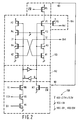
- FIG. 2 the relevant parts of the level shifter and the associated latch for use in the first voltage generating means are depicted.
- the shown circuit comprises control logic circuitry 161, a latch 162, level shifter 163 and supply transistor 164.
- control logic circuitry 161 a latch 162, level shifter 163 and supply transistor 164.
- latch 162 a latch 162
- level shifter 163 a latch 163
- supply transistor 164 a supply transistor 164.
- legend 100 the signs are shown to indicate the relevant voltages present in the circuit.
- the control logic circuitry 161 comprises: a NMOS-transistor N4, a control electrode of which is connected to a terminal of the first data input for receiving a relevant data-bit DI l ; a NMOS-transistor N5, a control electrode of which is connected to an associated column selection line (lines 91 or 92 in Figure 1) for receiving the column selection signal EL k ; a NMOS-transistor N6, a control electrode of which is connected to the load-latch line (line 93 in Figure 1) for receiving the load latch signal LL; a NMOS-transistor N3 and a PMOS-transistor P5 for receiving the write-enable signal EW transmitted by a not further described write enable circuit.
- the level shifter 163 comprises a first current path between supply voltage V DD and the negative high voltage V EE , constituted by the series arrangement of the conduction channels of PMOS-transistors P2, P4 and of the NMOS-transistors N4 and N2, and a second current path between supply terminal V DD and the negative high voltage V EE , constituted by the conduction channels of PMOS-transistors P1, P3 and NMOS-transistors N3, N1.
- a node J1 between transistors P4 and N4 is connected to the control electrode transistor N1; a node J2 between transistors P3 and N3 is connected to the control electrode of transistor N2.
- Transistors P1, N1 and N3 on the one hand and transistors P2, N2 and N4 on the other hand are mutually complementary controlled by the control logic circuitry 161 and the latch 162 disposed between the control logic circuitry 161 and level shifter 163. It is assumed that signal EW has been logic "1” formerly so that the present initial state of latch 162 is such that output Q is logic "0", and output Q is logic "1". Consequently, signal EW being returned to logic "0", the voltage at node J1 equals V EE and the voltage at node J2 equals VDD.
- latch 162 When signals LL, EL k and DI l are all logic “1", latch 162 is set to output a logic “0" at Q and a logic “1” at Q.
- the logic “1” at Q causes transistor P1 to block and the logic “0” at Q causes transistor P2 to conduct.
- the voltage at node J1 then slightly increases, whereupon transistor N1 will start to conduct, thereby lowering the voltage at node J2, as a consequence whereof transistor N2 will conduct less current. This process will cease in the event of node 32 being at V EE and node J1 being at V DD . Since terminal Q of latch 162 also controls supply transistor P6, which connects the supply line A kl , e.g.
- FIG 3 the relevant parts of the second voltage generating means are shown.
- the reference numerals in Figure 3 designate the parts and components corresponding to or identical to those of the previous Figure 2. The operation is similar to that of the circuit shown in Figure 2.
- the depicted second voltage generating means comprises control logic circuitry 151, a latch 152 and a level shifter 153.
- the control electrode of transistor N4 is connected to the output of a NOR-gate (not shown), that receives the respective bits to be written into the respective bit cells of the selected memory location. Unless all bits are logic "0" the latch will not be set and will output a logic "0" at Q and a logic "1" at Q .
- node J2 will carry signal EE k being a logic "1" at supply voltage level V DD , thereby blocking the second switching transistor in the switch accompanying the relevant memory location, e.g. transistor 17b in switch 17 of memory location 10 in Figure 1.
- Output Q of latch 152 is connected to the first switch transistor in said switch (transistor 17a in switch 17) and will render said transistor conductive by signal EE k being equal to V SS .
- the activation line activation line 16
- the latch is set to output a logic "1” at Q and a logic "0" at Q . Consequently signal EE k is at V EE switching the second switch transistor (e.g. switch transistor 17b in Figure 1) on, while signal EE k is at V DD thereby blocking the first switching transistor (e.g. switching transistor 17a).
- the latches 152 and 162 not only function as elements having a memory function, but also as to output mutually complementary signals in order to control the parallel current paths in the relevant level shifter 153 and 163, respectively.
- the arrangement of the control logic circuitry, the latch and the level shifter in the way shown, offers a very compact building block for a memory of the kind set forth.
Landscapes
- Engineering & Computer Science (AREA)
- Microelectronics & Electronic Packaging (AREA)
- Computer Hardware Design (AREA)
- Read Only Memory (AREA)
Claims (8)
- Circuit de mémoire intégré comprenant une mémoire EEPROM comportant une pluralité de sections (10/30/50/60; 20/40/70/80), chaque section particulière desdites sections comprenant :- une pluralité de lignes de cellules de mémoire (10a; 10b) agencées en une pluralité de colonnes, et- des moyens de programmation (50/60) dur programmer des cellules sélectionnées parmis lesdites cellules de mémoire sous la commande d'une pluralité de données respectives délivrées en parallèle à une pluralité de noeuds d'entrée de données respectifs (61a, 61b); circuit dans lequel :- chaque colonne respective desdites colonnes comprend une première ligne de commande respective (14a; 14b) et une deuxième ligne de commande respective (13a; 13b);- chaque cellule de mémoire de la colonne respective est couplée entre la première ligne et la deuxième ligne de commande respectives;- chaque cellule de mémoire comprend un transistor programmable (11a; 11b) et un transistor d'accès (12a; 12b) avec des canaux de conduction agencés en série;- des électrodes de commande des transistors d'accès d'une ligne respective parmis lesdites lignes sont couplées à une ligne de mots respective (15);caractérisé en ce que :- dans chaque cellule de la colonne respective, le transistor d'accès a son canal de conduction couplé à la première ligne de commande respective et le transistor programmable a son canal de conduction couplé à la deuxième ligne de commande respective;- les moyens de programmation de la section particulière comprennent :- une pluralité de circuits de programmation uniformes, à raison d'un respectivement pour chaque colonne, chaque circuit de programmation comprenant :- un décaleur de niveau respectif (63a; 63b) ayant une entrée couplée à un noeud respectif desdits noeuds d'entrée de données et ayant une sortie connectée à la première ligne de commande et étant à même de fournir soit une tension de programmation de haut niveau (VEE), soit une tension d'alimentation de bas niveau (VDD) sous la commande des données respectives;- un premier moyen de commutation (64a; 64b) étant agencé entre une borne d'alimentation (VDD) et la deuxième ligne de commande et étant à même de connecter la deuxième ligne de commande à la tension d'alimentation sous la commande des données respectives au noeud d'entrée de données respectif;- un moyen de détection à porte (50) ayant une entrée de détection connectée aux noeuds d'entrée de données de la section et étant à même de fournir un signal de sortie indiquant un niveau logique prédéterminé des données présentes aux noeuds d'entrée de données;- une pluralité de deuxièmes moyens de commutation (17), un pour chaque ligne de la section, pour alimenter les électrodes de commande des transistors programmables avec soit la tension de programmation de haut niveau en présence du niveau logique prédéterminé des données, soit la tension d'alimentation sous la commande du moyen de détection à porte.
- Circuit selon la revendication 1, caractérisé en ce que le moyen de détection à porte est à même de fournir le signal de sortie si la pluralité de données de niveau logique prédéterminé ont toutes le même niveau logique.
- Circuit selon la revendication 1, caractérisé en ce que les moyens de programmation de la pluralité de sections peuvent être activés en parallèle.
- Circuit selon la revendication 1, caractérisé en ce que chaque noeud d'entrée de données respectif est couplé au décaleur de niveau respectif via un verrou respectif (62a; 62b; 162).
- Circuit selon la revendication 4, caractérisé en ce que le décaleur de niveau respectif comprend :- un premier trajet de courant avec un canal de conduction d'un premier transistor (P2) connecté à la tension d'alimentation et avec un canal de conduction d'un deuxième transistor (N2) connecté à la tension de programmation;- un deuxième trajet de courant avec un canal de conduction d'un troisième transistor (P1) couplé à la tension d'alimentation et avec un canal de conduction d'un quatrième transistor (N1) connecté à la tension de programmation;circuit dans lequel :- un premier noeud (J1) entre le premier transistor et le deuxième transistor est couplé à une électrode de commande du quatrième transistor;- un deuxième noeud (J2) entre le troisième transistor et le quatrième transistor est couplé à une électrode de commande du deuxième transistor;- des électrodes de commande du premier transistor et du troisième transistor sont couplées au noeud d'entrée de données respectif via le verrou (62a; 162) pour une commande mutuellement complémentaire;- un cinquième transistor (64a, P6) est agencé entre la borne de tension d'alimentation et la deuxième ligne de commande (13a; Akl);- le deuxième noeud est connecté à la première ligne de commande (14a; Bkl);- le premier transistor, le troisième transistor et le cinquième transistor sont d'un premier type de conductivité;- le deuxième transistor et le quatrième transistor sont d'un deuxième type de conductivité.
- Circuit selon la revendication 1, dans lequel le moyen de détection à porte comprend :- une porte logique (51) comportant une pluralité d'entrées respectives connectées aux noeuds d'entrée de données respectifs;- un autre décaleur de niveau (53) ayant une entrée couplée à une sortie de la grille logique, et dans lequel le deuxième moyen de commutation comprend :- un commutateur supérieur (17a) agencé entre la borne de tension d'alimentation et un noeud (16) connecté aux électrodes de commande des transistors programmables et couplé de manière contrôlable à la sortie de l'autre décaleur de niveau, et- un commutateur inférieur (17b) agencé entre ledit noeud et la ligne de mots et qui est couplé de manière contrôlable à la sortie de la porte logique.
- Circuit selon la revendication 6, dans lequel la porte logique est couplée à l'autre décaleur de niveau via un verrou (52).
- Circuit selon la revendication 7, dans lequel l'autre décaleur de niveau comprend :- un premier trajet de courant avec un canal de conduction d'un premier transistor (P2) connecté à la tension d'alimentation et avec un canal de conduction d'un deuxième transistor (N2) connecté à la tension de programmation;- un deuxième trajet de courant avec un canal de conduction d'un troisième transistor (P1) couplé à la tension d'alimentation et avec un canal de conduction d'un quatrième transistor (N1) connecté à la tension de programmation;circuit dans lequel :- un premier noeud (J1) entre le premier transistor et le deuxième transistor est couplé à une électrode de commande du quatrième transistor;- un deuxième noeud (J2) entre le troisième transistor et le quatrième transistor est couplé à une électrode de commande du deuxième transistor;- les électrodes de commande du premier transistor et du troisième transistor sont couplées au verrou (52; 152) pour une commande mutuellement complémentaire;- l'électrode de commande du troisième transistor est connectée pour commander le commutateur supérieur (17a);- le deuxième noeud est connecté pour commander le commutateur inférieur (17b);- le premier transistor et le troisième transistor sont d'un premier type de conductivité, et- le deuxième transistor et le quatrième transistor sont d'un deuxième type de conductivité.
Applications Claiming Priority (2)
| Application Number | Priority Date | Filing Date | Title |
|---|---|---|---|
| NL8800583 | 1988-03-09 | ||
| NL8800583 | 1988-03-09 |
Publications (3)
| Publication Number | Publication Date |
|---|---|
| EP0332274A2 EP0332274A2 (fr) | 1989-09-13 |
| EP0332274A3 EP0332274A3 (fr) | 1991-10-09 |
| EP0332274B1 true EP0332274B1 (fr) | 1994-06-22 |
Family
ID=19851909
Family Applications (1)
| Application Number | Title | Priority Date | Filing Date |
|---|---|---|---|
| EP89200552A Expired - Lifetime EP0332274B1 (fr) | 1988-03-09 | 1989-03-06 | EEPROM à mode d'effacement et d'écriture commandé par des données |
Country Status (4)
| Country | Link |
|---|---|
| EP (1) | EP0332274B1 (fr) |
| JP (1) | JP2847141B2 (fr) |
| KR (1) | KR0153518B1 (fr) |
| DE (1) | DE68916281T2 (fr) |
Families Citing this family (5)
| Publication number | Priority date | Publication date | Assignee | Title |
|---|---|---|---|---|
| JPH03232196A (ja) * | 1990-02-07 | 1991-10-16 | Toshiba Corp | 半導体記憶装置 |
| KR940004404B1 (ko) * | 1990-11-30 | 1994-05-25 | 삼성전자 주식회사 | 불휘발성 반도체 메모리장치 |
| FR2735896B1 (fr) * | 1995-06-21 | 1997-08-22 | Sgs Thomson Microelectronics | Memoire eeprom programmable et effacable par effet de fowler-nordheim |
| DE19730116C2 (de) | 1997-07-14 | 2001-12-06 | Infineon Technologies Ag | Halbleiterspeicher mit nicht-flüchtigen Zwei-Transistor-Speicherzellen |
| KR102245674B1 (ko) | 2017-11-17 | 2021-04-27 | 주식회사 엘지화학 | 고상 추출용 마이크로 디바이스 |
Family Cites Families (4)
| Publication number | Priority date | Publication date | Assignee | Title |
|---|---|---|---|---|
| US3938108A (en) * | 1975-02-03 | 1976-02-10 | Intel Corporation | Erasable programmable read-only memory |
| US4442510A (en) * | 1981-12-28 | 1984-04-10 | National Semiconductor Corporation | Semiconductor memory byte clear circuit |
| US4566080A (en) * | 1983-07-11 | 1986-01-21 | Signetics Corporation | Byte wide EEPROM with individual write circuits |
| JPH0736274B2 (ja) * | 1985-10-08 | 1995-04-19 | 日本電気株式会社 | 読出し専用メモリ |
-
1989
- 1989-03-06 DE DE68916281T patent/DE68916281T2/de not_active Expired - Fee Related
- 1989-03-06 EP EP89200552A patent/EP0332274B1/fr not_active Expired - Lifetime
- 1989-03-09 KR KR1019890002878A patent/KR0153518B1/ko not_active Expired - Fee Related
- 1989-03-09 JP JP5523189A patent/JP2847141B2/ja not_active Expired - Fee Related
Also Published As
| Publication number | Publication date |
|---|---|
| DE68916281T2 (de) | 1995-01-26 |
| EP0332274A3 (fr) | 1991-10-09 |
| JP2847141B2 (ja) | 1999-01-13 |
| DE68916281D1 (de) | 1994-07-28 |
| EP0332274A2 (fr) | 1989-09-13 |
| JPH0214494A (ja) | 1990-01-18 |
| KR890015279A (ko) | 1989-10-28 |
| KR0153518B1 (ko) | 1998-12-01 |
Similar Documents
| Publication | Publication Date | Title |
|---|---|---|
| KR100724815B1 (ko) | 저항성 메모리 장치, 기록 방법, 판독 방법, 소거 방법 및메모리 장치 동작 방법 | |
| US6055187A (en) | Sensing circuitry for reading and verifying the contents of electrically programmable/erasable non-volatile memory cells | |
| US4937787A (en) | Programmable read only memory with means for discharging bit line before program verifying operation | |
| US4543647A (en) | Electrically programmable non-volatile semiconductor memory device | |
| US5369609A (en) | Floating gate memory array with latches having improved immunity to write disturbance, and with storage latches | |
| US4905197A (en) | Semiconductor memory having circuitry for discharging a digit line before verifying operation | |
| EP0597231A2 (fr) | Amplificateur de détection ayant des circuits de commande d'écriture locaux | |
| US4933906A (en) | Non-volatile semiconductor memory device | |
| EP0459794B1 (fr) | Dispositif de mémoire morte | |
| US4631707A (en) | Memory circuit with power supply voltage detection means | |
| US4870618A (en) | Semiconductor memory equipped with test circuit for testing data holding characteristic during data programming period | |
| US4864541A (en) | Integrated circuit of the logic circuit type comprising an electrically programmable non-volatile memory | |
| EP0131343B1 (fr) | Circuit pour l'écrituure "un pas" des EEPROMS | |
| EP0361561B1 (fr) | Circuit intégré de mémorisation muni d'une entrée et d'une sortie parallèles et série | |
| US5644529A (en) | Integrated circuit for the programming of a memory cell in a non-volatile memory register | |
| US5390150A (en) | Semiconductor memory device with redundancy structure suppressing power consumption | |
| EP0945874B1 (fr) | Dispositif de mémoire non volatile à semi-conducteurs | |
| US20040076029A1 (en) | Data sensing circuits and methods for magnetic memory devices | |
| EP0332274A2 (fr) | EEPROM à mode d'effacement et d'écriture commandé par des données | |
| US20010014036A1 (en) | Lock bit for an electrically erasable memory word | |
| US6466508B1 (en) | Semiconductor memory device having high-speed read function | |
| JP3099563B2 (ja) | 半導体記憶装置 | |
| US5396469A (en) | SRAM memory requiring reduced voltage swing during write | |
| US5946241A (en) | Non-volatile memory in integrated circuit form with fast reading | |
| US5991199A (en) | Device and method for the programming of a memory |
Legal Events
| Date | Code | Title | Description |
|---|---|---|---|
| PUAI | Public reference made under article 153(3) epc to a published international application that has entered the european phase |
Free format text: ORIGINAL CODE: 0009012 |
|
| AK | Designated contracting states |
Kind code of ref document: A2 Designated state(s): CH DE FR GB IT LI |
|
| PUAL | Search report despatched |
Free format text: ORIGINAL CODE: 0009013 |
|
| AK | Designated contracting states |
Kind code of ref document: A3 Designated state(s): CH DE FR GB IT LI |
|
| 17P | Request for examination filed |
Effective date: 19920409 |
|
| 17Q | First examination report despatched |
Effective date: 19930312 |
|
| GRAA | (expected) grant |
Free format text: ORIGINAL CODE: 0009210 |
|
| AK | Designated contracting states |
Kind code of ref document: B1 Designated state(s): CH DE FR GB IT LI |
|
| REF | Corresponds to: |
Ref document number: 68916281 Country of ref document: DE Date of ref document: 19940728 |
|
| ITF | It: translation for a ep patent filed | ||
| ET | Fr: translation filed | ||
| ITPR | It: changes in ownership of a european patent |
Owner name: CAMBIO RAGIONE SOCIALE;PHILIPS ELECTRONICS N.V. |
|
| PLBE | No opposition filed within time limit |
Free format text: ORIGINAL CODE: 0009261 |
|
| STAA | Information on the status of an ep patent application or granted ep patent |
Free format text: STATUS: NO OPPOSITION FILED WITHIN TIME LIMIT |
|
| REG | Reference to a national code |
Ref country code: FR Ref legal event code: CD |
|
| 26N | No opposition filed | ||
| REG | Reference to a national code |
Ref country code: FR Ref legal event code: CD |
|
| PGFP | Annual fee paid to national office [announced via postgrant information from national office to epo] |
Ref country code: CH Payment date: 19990217 Year of fee payment: 11 |
|
| PG25 | Lapsed in a contracting state [announced via postgrant information from national office to epo] |
Ref country code: LI Free format text: LAPSE BECAUSE OF NON-PAYMENT OF DUE FEES Effective date: 20000331 Ref country code: CH Free format text: LAPSE BECAUSE OF NON-PAYMENT OF DUE FEES Effective date: 20000331 |
|
| REG | Reference to a national code |
Ref country code: CH Ref legal event code: PL |
|
| REG | Reference to a national code |
Ref country code: CH Ref legal event code: AUV Free format text: DAS OBENGENANNTE PATENT IST, MANGELS BEZAHLUNG DER 12. JAHRESGEBUEHR, INNERT DER GESETZLICHEN FRIST, DURCH VERFUEGUNG VOM 31. OKTOBER 2000 ERLOSCHEN. |
|
| REG | Reference to a national code |
Ref country code: GB Ref legal event code: IF02 |
|
| PGFP | Annual fee paid to national office [announced via postgrant information from national office to epo] |
Ref country code: FR Payment date: 20030328 Year of fee payment: 15 |
|
| PGFP | Annual fee paid to national office [announced via postgrant information from national office to epo] |
Ref country code: GB Payment date: 20030331 Year of fee payment: 15 |
|
| PGFP | Annual fee paid to national office [announced via postgrant information from national office to epo] |
Ref country code: DE Payment date: 20030515 Year of fee payment: 15 |
|
| PG25 | Lapsed in a contracting state [announced via postgrant information from national office to epo] |
Ref country code: GB Free format text: LAPSE BECAUSE OF NON-PAYMENT OF DUE FEES Effective date: 20040306 |
|
| PG25 | Lapsed in a contracting state [announced via postgrant information from national office to epo] |
Ref country code: DE Free format text: LAPSE BECAUSE OF NON-PAYMENT OF DUE FEES Effective date: 20041001 |
|
| GBPC | Gb: european patent ceased through non-payment of renewal fee | ||
| PG25 | Lapsed in a contracting state [announced via postgrant information from national office to epo] |
Ref country code: FR Free format text: LAPSE BECAUSE OF NON-PAYMENT OF DUE FEES Effective date: 20041130 |
|
| REG | Reference to a national code |
Ref country code: FR Ref legal event code: ST |
|
| PG25 | Lapsed in a contracting state [announced via postgrant information from national office to epo] |
Ref country code: IT Free format text: LAPSE BECAUSE OF NON-PAYMENT OF DUE FEES Effective date: 20050306 |