EP0332448B1 - Dispositif de supraconducteurs opto-électroniques - Google Patents
Dispositif de supraconducteurs opto-électroniques Download PDFInfo
- Publication number
- EP0332448B1 EP0332448B1 EP89302357A EP89302357A EP0332448B1 EP 0332448 B1 EP0332448 B1 EP 0332448B1 EP 89302357 A EP89302357 A EP 89302357A EP 89302357 A EP89302357 A EP 89302357A EP 0332448 B1 EP0332448 B1 EP 0332448B1
- Authority
- EP
- European Patent Office
- Prior art keywords
- superconductive
- photoconductive
- region
- chemical formula
- general chemical
- Prior art date
- Legal status (The legal status is an assumption and is not a legal conclusion. Google has not performed a legal analysis and makes no representation as to the accuracy of the status listed.)
- Expired - Lifetime
Links
- 230000005693 optoelectronics Effects 0.000 title claims description 46
- 239000000463 material Substances 0.000 claims description 69
- 239000000126 substance Substances 0.000 claims description 26
- 239000000758 substrate Substances 0.000 claims description 9
- 239000000470 constituent Substances 0.000 claims description 2
- WMWLMWRWZQELOS-UHFFFAOYSA-N bismuth(iii) oxide Chemical compound O=[Bi]O[Bi]=O WMWLMWRWZQELOS-UHFFFAOYSA-N 0.000 description 44
- 230000003287 optical effect Effects 0.000 description 28
- 229910002480 Cu-O Inorganic materials 0.000 description 26
- 230000007704 transition Effects 0.000 description 21
- 230000005284 excitation Effects 0.000 description 17
- 239000013558 reference substance Substances 0.000 description 16
- 239000000919 ceramic Substances 0.000 description 12
- 230000004044 response Effects 0.000 description 12
- 239000013078 crystal Substances 0.000 description 10
- 230000000694 effects Effects 0.000 description 10
- 239000010410 layer Substances 0.000 description 10
- 229910009203 Y-Ba-Cu-O Inorganic materials 0.000 description 9
- 239000002772 conduction electron Substances 0.000 description 5
- 238000002474 experimental method Methods 0.000 description 5
- 239000011521 glass Substances 0.000 description 5
- 239000012212 insulator Substances 0.000 description 5
- 229910052760 oxygen Inorganic materials 0.000 description 5
- 238000010521 absorption reaction Methods 0.000 description 4
- 239000000969 carrier Substances 0.000 description 4
- 230000000295 complement effect Effects 0.000 description 4
- 238000010586 diagram Methods 0.000 description 4
- 239000002887 superconductor Substances 0.000 description 4
- 238000004458 analytical method Methods 0.000 description 3
- QVGXLLKOCUKJST-UHFFFAOYSA-N atomic oxygen Chemical compound [O] QVGXLLKOCUKJST-UHFFFAOYSA-N 0.000 description 3
- BERDEBHAJNAUOM-UHFFFAOYSA-N copper(I) oxide Inorganic materials [Cu]O[Cu] BERDEBHAJNAUOM-UHFFFAOYSA-N 0.000 description 3
- KRFJLUBVMFXRPN-UHFFFAOYSA-N cuprous oxide Chemical compound [O-2].[Cu+].[Cu+] KRFJLUBVMFXRPN-UHFFFAOYSA-N 0.000 description 3
- 230000005283 ground state Effects 0.000 description 3
- 230000020169 heat generation Effects 0.000 description 3
- 230000007246 mechanism Effects 0.000 description 3
- 239000001301 oxygen Substances 0.000 description 3
- VYPSYNLAJGMNEJ-UHFFFAOYSA-N Silicium dioxide Chemical compound O=[Si]=O VYPSYNLAJGMNEJ-UHFFFAOYSA-N 0.000 description 2
- 230000008859 change Effects 0.000 description 2
- 230000001427 coherent effect Effects 0.000 description 2
- 238000011161 development Methods 0.000 description 2
- 230000003993 interaction Effects 0.000 description 2
- 230000001404 mediated effect Effects 0.000 description 2
- 239000000203 mixture Substances 0.000 description 2
- 239000011224 oxide ceramic Substances 0.000 description 2
- 229910052574 oxide ceramic Inorganic materials 0.000 description 2
- 238000010587 phase diagram Methods 0.000 description 2
- 230000010287 polarization Effects 0.000 description 2
- 230000009897 systematic effect Effects 0.000 description 2
- CMSGUKVDXXTJDQ-UHFFFAOYSA-N 4-(2-naphthalen-1-ylethylamino)-4-oxobutanoic acid Chemical compound C1=CC=C2C(CCNC(=O)CCC(=O)O)=CC=CC2=C1 CMSGUKVDXXTJDQ-UHFFFAOYSA-N 0.000 description 1
- 229920002799 BoPET Polymers 0.000 description 1
- 230000005536 Jahn Teller effect Effects 0.000 description 1
- 230000005668 Josephson effect Effects 0.000 description 1
- 239000005041 Mylar™ Substances 0.000 description 1
- 229910002370 SrTiO3 Inorganic materials 0.000 description 1
- 239000000956 alloy Substances 0.000 description 1
- 229910045601 alloy Inorganic materials 0.000 description 1
- 238000003491 array Methods 0.000 description 1
- 238000004364 calculation method Methods 0.000 description 1
- 150000001768 cations Chemical class 0.000 description 1
- 229910052681 coesite Inorganic materials 0.000 description 1
- 229910052906 cristobalite Inorganic materials 0.000 description 1
- 230000007423 decrease Effects 0.000 description 1
- 230000005281 excited state Effects 0.000 description 1
- 230000006872 improvement Effects 0.000 description 1
- 230000006698 induction Effects 0.000 description 1
- 239000004615 ingredient Substances 0.000 description 1
- 230000010354 integration Effects 0.000 description 1
- 229920000126 latex Polymers 0.000 description 1
- WABPQHHGFIMREM-UHFFFAOYSA-N lead(0) Chemical compound [Pb] WABPQHHGFIMREM-UHFFFAOYSA-N 0.000 description 1
- 238000004519 manufacturing process Methods 0.000 description 1
- 239000002184 metal Substances 0.000 description 1
- 229910052751 metal Inorganic materials 0.000 description 1
- 150000002739 metals Chemical class 0.000 description 1
- 238000000034 method Methods 0.000 description 1
- 230000000704 physical effect Effects 0.000 description 1
- 238000011160 research Methods 0.000 description 1
- 239000000377 silicon dioxide Substances 0.000 description 1
- 235000012239 silicon dioxide Nutrition 0.000 description 1
- 230000003595 spectral effect Effects 0.000 description 1
- 238000001228 spectrum Methods 0.000 description 1
- 229910052682 stishovite Inorganic materials 0.000 description 1
- 238000006467 substitution reaction Methods 0.000 description 1
- 239000002344 surface layer Substances 0.000 description 1
- 230000002459 sustained effect Effects 0.000 description 1
- 238000012360 testing method Methods 0.000 description 1
- 229910052905 tridymite Inorganic materials 0.000 description 1
Images








Classifications
-
- H—ELECTRICITY
- H10—SEMICONDUCTOR DEVICES; ELECTRIC SOLID-STATE DEVICES NOT OTHERWISE PROVIDED FOR
- H10N—ELECTRIC SOLID-STATE DEVICES NOT OTHERWISE PROVIDED FOR
- H10N60/00—Superconducting devices
- H10N60/10—Junction-based devices
- H10N60/128—Junction-based devices having three or more electrodes, e.g. transistor-like structures
-
- H—ELECTRICITY
- H10—SEMICONDUCTOR DEVICES; ELECTRIC SOLID-STATE DEVICES NOT OTHERWISE PROVIDED FOR
- H10N—ELECTRIC SOLID-STATE DEVICES NOT OTHERWISE PROVIDED FOR
- H10N60/00—Superconducting devices
- H10N60/80—Constructional details
- H10N60/84—Switching means for devices switchable between superconducting and normal states
-
- Y—GENERAL TAGGING OF NEW TECHNOLOGICAL DEVELOPMENTS; GENERAL TAGGING OF CROSS-SECTIONAL TECHNOLOGIES SPANNING OVER SEVERAL SECTIONS OF THE IPC; TECHNICAL SUBJECTS COVERED BY FORMER USPC CROSS-REFERENCE ART COLLECTIONS [XRACs] AND DIGESTS
- Y10—TECHNICAL SUBJECTS COVERED BY FORMER USPC
- Y10S—TECHNICAL SUBJECTS COVERED BY FORMER USPC CROSS-REFERENCE ART COLLECTIONS [XRACs] AND DIGESTS
- Y10S505/00—Superconductor technology: apparatus, material, process
- Y10S505/70—High TC, above 30 k, superconducting device, article, or structured stock
- Y10S505/701—Coated or thin film device, i.e. active or passive
-
- Y—GENERAL TAGGING OF NEW TECHNOLOGICAL DEVELOPMENTS; GENERAL TAGGING OF CROSS-SECTIONAL TECHNOLOGIES SPANNING OVER SEVERAL SECTIONS OF THE IPC; TECHNICAL SUBJECTS COVERED BY FORMER USPC CROSS-REFERENCE ART COLLECTIONS [XRACs] AND DIGESTS
- Y10—TECHNICAL SUBJECTS COVERED BY FORMER USPC
- Y10S—TECHNICAL SUBJECTS COVERED BY FORMER USPC CROSS-REFERENCE ART COLLECTIONS [XRACs] AND DIGESTS
- Y10S505/00—Superconductor technology: apparatus, material, process
- Y10S505/70—High TC, above 30 k, superconducting device, article, or structured stock
- Y10S505/701—Coated or thin film device, i.e. active or passive
- Y10S505/702—Josephson junction present
-
- Y—GENERAL TAGGING OF NEW TECHNOLOGICAL DEVELOPMENTS; GENERAL TAGGING OF CROSS-SECTIONAL TECHNOLOGIES SPANNING OVER SEVERAL SECTIONS OF THE IPC; TECHNICAL SUBJECTS COVERED BY FORMER USPC CROSS-REFERENCE ART COLLECTIONS [XRACs] AND DIGESTS
- Y10—TECHNICAL SUBJECTS COVERED BY FORMER USPC
- Y10S—TECHNICAL SUBJECTS COVERED BY FORMER USPC CROSS-REFERENCE ART COLLECTIONS [XRACs] AND DIGESTS
- Y10S505/00—Superconductor technology: apparatus, material, process
- Y10S505/70—High TC, above 30 k, superconducting device, article, or structured stock
- Y10S505/701—Coated or thin film device, i.e. active or passive
- Y10S505/703—Microelectronic device with superconducting conduction line
Definitions
- This invention relates to a superconductive optoelectronic device.
- the superconductive optoelectronic device of the invention is novel and vastly different from those of prior art in that the invention uses a combination of superconductive material and special superconductive photoconductive-material which reveals photoconductivity below the critical temperature of the relevant superconductive material.
- a number of new electronic devices and optoelectronic apparatuses may be developed, for instance, a switching device with no power loss, an optically operating device with no power loss, an optically operating logical device, a space parallel type optically operating apparatus, a camera or an image forming device possibly with superconducting wiring, a high-speed optically operating apparatus to be driven at an extremely low power, and the like.
- the superconductive photoconductive-oxide materials are so far electric insulators at room temperature, but when they are cooled down to the temperatures below the transition points of superconductive materials related to them, they reveal photoconductivity, i.e., they produce photo carriers and their conductivity varies depending on the intensity of the excitation light which is incident thereto.
- a power-loss-free useful superconductive optoelectronic device can be formed by combining a superconductive photoconductive-material of for instance the Ca-Sr-Bi-Cu-O system with its related superconductive material of for instance the Ca-Sr-Bi-Cu-O system.
- superconductive optoelectronic device is an optoelectronic device made of a combination of a superconductive material of one oxide system and the superconductive-conjugate photoconductive-material of the same oxide system which reveals photoconductivity at temperatures below the critical temperatures of the superconductive material.
- An object of the invention is to provide a novel superconductive optoelectronic device by using effectively the optical properties of that superconductive-conjugate photoconductive-material which is discovered by the inventor.
- the invention is neither a mere improvement of the prior art nor a simple solution of problems existing in the prior art, but an entirely new achievement.
- a superconductive optoelectronic device as characterised in claim 1 comprises a substrate, a photoconductive gate region formed on the substrate, and a source region and a drain region formed on the substrate at opposite sides of the gate region respectively so as to face toward each other across the gate region.
- the source and drain regions are made of a superconductive material
- the gate region is made of a superconductive-conjugate photoconductive-material which reveals photoconductivity at temperatures below the critical temperature for superconductivity of the superconductive material
- the superconductive-conjugate photoconductive-material and the superconductive material are of the same general chemical formula but with different contents of constituent elements.
- Bias source may be connected across the source region and the drain region of the optoelectronic devices of the invention, so as to drive an electric current through its photoconductive gate region depending on the intensity of light which is incident to the photoconductive gate region.
- 1 is a substrate, 2 a gate region, 3 a source region, 4 a drain region, 5 an insulating layer, 6 a conductive glass layer, 10 an alley-like light source, 11 a coding image-mask pattern, 12 a correlative image screen, and 13 is a decoding mask optical element alley.
- the inventor's experiments and analyses on the photoconductivity and superconductivity of various superconductive materials showed that a certain portions of superconductive materials in their phase diagram reveal photoconductivity complementary to or as well as superconductivity at temperature below their regions of transition temperatures from normal conductivity to superconductivity. For instance, in the case of superconductive oxides of the Ca-Sr-Bi-Cu-O system, the inventors discovered that with changing Sr content their superconductivity can be converted into photoconductivity at temperatures below their critical temperatures.
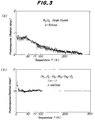
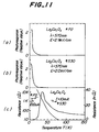
- Figure 1 illustrates typical results of experiments on the superconductivity and photoconductivity of the Ca-Sr-Bi-Cu-O system oxides.
- the curve (a) in Fig. 1 shows the temperature dependence of photoconductivity of Bi2O3 ceramics which is a reference substance clarified by the inventor.
- the Ca-Sr-Bi-Cu-O system reveals superconductivity if, e.g., its content x of Sr is in the range of 0.7 ⁇ 1 ⁇ x ⁇ 2, and if its content x of Sr is smaller than 0.7 ⁇ 1 such superconductivity disappears and it reveals complementary photoconductivity at temperature regions below their transition temperatures.
- an optoelectronic element of FET-like shape is formed by making a gate region with a superconductive photoconductive-material while making a source region and a drain region with a relevant superconductive material, an output current whose magnitude varies depending on the wavelength and intensity of light incident to the gate region can be produced so as to flow across the source and drain regions. If such an optoelectronic device is sustained at a temperature below the transition temperature of its superconductive material, it must work as a superconductive optoelectronic device which can be used in numerous ways; for instance, as a power-loss-free optical switching device with high-speed response, an optical detector, an optical signals amplifying device, or the like.
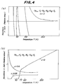
- Fig. 6 shows test results on its superconductivity and photoconductivity.
- z ⁇ 6.5 is a merely rough indication of the boundary not clearly and should not be taken exactly, since the superconductive defined photoconductive-area are continuously close to the superconductive-areas in thier phase diagram. Similar situations are the cases also for the other systems as far as the oxygen content z concerns.
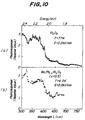
- Oxide material of Ba-Pb-Bi-O system will be described now by referring to Fig. 9 and Fig. 10.
- Curves (a) and (b) in Fig. 9 show the temperature dependences of photoresponse Q (T, ⁇ ) of a reference substance Bi2O3 ceramics and oxide specimens with a general chemical formula of Ba1-Pb 1-x -Bi x -O z , respectively.
- the inventor found that they reveal superconductivity under the conditions of 0.20 ⁇ x ⁇ 0.35 and 2.81 ⁇ z ⁇ 3, while they reveal photoconductivity under the conditions of x ⁇ 0.35 and 2.7 ⁇ z ⁇ 2.81.
- Fig. 13 shows the relationship between the photoconductivity and the quantity of incident light (i.e., excitation light intensity) for the above oxide with z ⁇ 3.88. It can be seen from Fig. 13 that the photoresponse current clearly increases with the intensity of incident light.
- Fig. 14 is a schematic diagram showing the structure of an embodiment of the superconductive optoelectronic device according to the invention.
- the embodiment is a superconductive phototransistor in which a positive gate voltage V G is used (V G ⁇ 0).
- a substrate 1 is made of SrTiO3, and a photoconductive gate region 2 is formed on the substrate 1 with superconductive photoconductive-material Ca2-Bi1-Cu2-O z .
- the photoconductive gate region 2 has a width of 0.2 ⁇ m to 1.0 mm and a thickness of 1-10 ⁇ m.
- the above superconductive photoconductive-material Ca2-Bi1-Cu2-O z reveals photoconductivity in response to excitation by incident light of wavelength at least ⁇ 540-740 nm at a temperature below the transition temperature of a superconductive substance Ca1-Sr1-Bi1-Cu2-O z .
- a source region 3 and a drain region 4 are formed with Ca1-Sr1- Bi1-Cu2-O z oxide which reveals superconductivity below its critical temperature of 80K or 105-115 K.
- An electrically insulating layer 5 which is optically transparent is formed so as to cover top surfaces of the gate region 2, the source region 3, and the drain region 4.
- the insulating layer 5 of the illustrated example was a 1 ⁇ m thick SiO2 film or mylar sheet. Further, a conductive surface of glass layer 6, for instance made of a NESA (Trademark of Pittsburgh Plate Glass Company) glass layer, is placed on the insulating layer 5, and electrodes are deposited on the conductive surface of glass layer 6.
- NESA Trademark of Pittsburgh Plate Glass Company
- a source for bias voltage V G is connected across the source region 3 and electrodes of the conductive surface of glass layer and a source for source-drain voltage V SD is connected between the source region 3 and the drain region 4 across the gate region 2.
- the superconducting optoelectronic element of Fig. 14 is cooled to a temperature below the critical temperatures, i.e., about 80K or 105-115K, of the superconducting zones of Ca 2-x -Sr x -Bi1-Cu2-O z and excitation light signals in a wavelength range is irradiated to the gate region 2.
- a pulsed dye laser of 3 nsec width can be used for an excitation light source. This fact basically indicates a high speed response of the device itself.
- photocarriers are generated in the gate region 2 depending on the photon number or intensity of light incident thereto.
- the generated carriers are accelerated by the source-drain voltage V SD so as to produce an induced output current which is delivered to an output resistor R. Accordingly, an output voltage due to incident photosignals appears across the resistor R.
- the amount and density of optically excited carriers in the gate region 2 can be variable depending not only on the photon number or intensity of incident light thereto but also the bias voltage V G , and the bias voltage V G can be harmoniously adjusted so as to meet specific requirements from users .
- photocarrier density of the order e.g., of 101/cm3 can be obtainable in a surface layer of the gate region 2.
- the superconducting optoelectronic device of Fig. 14 can be used as a superconductive switching device.
- the source region 3 and the drain region 4 made of superconductive material are free from heat generation during operation, so that the optoelectronic device of Fig. 14 possesses those advantages which are inherent to superconductivity.
- Fig. 15 is a partial schematic diagram of an embodiment of the superconductive optoelectronic device of the invention, in which device a number of the superconductive optoelectronic devices of Fig. 14 are integrated at a high density in the form of one- or two-dimensional arrays. If wiring among different devices in the device of Fig. 15 is made by using superconducting material, heat generation in the array or apparatus can be suppressed to an extremely low level.
- the superconducting optoelectronic device and apparatus of the invention can be used in various fields; for instance, as a loss-free pick up (or camera) devices, loss-free detectors of optical signals in an optical computer which executes parallel operations in a spatially arranged manner, and the like.
- the device of the invention can be also used in a multiple channel system which selectively utilizes a number of different wavelengths in the incident light.
- Fig. 16 schematically illustrates an optical calculation procedure in a projection-correlative optical system of a space parallel optical computer in which system the superconductive optoelectronic devices of the invention are used.
- An array-like light source 10 projects a number of operation beams in parallel onto an encoded mask pattern 11.
- the mask pattern 11 carries encoded image signals corresponding to an input signal, said encoded image signal responding to the type of operation to be carried out by the light beams.
- the light beams After passing through the mask pattern 11, the light beams pass a correlative image screen 12 and then enter in parallel into the corresponding devices in a decoding mask optical device array 13.
- Each optical device receives a coded signal which is modulated by the mask screen, and operated results can be obtained from the optoelectronic output signals from each of the optical devices. If each optical device of the decoding mask optical device array 13 is the superconductive optoelectronic device of the invention, parallel optical operations can be effected while minimizing heat generation during the operation.
- the illustrated embodiment of the invention is made by using the Ca-Sr-Bi-Cu-O system oxides, but other superconductive photoconductive-materials such as those of the Ba-Pb-Bi-O system, La-Cu-O system, or Y-Ba-Cu-O system can be also used to form the superconducting optoelectronic device and apparatus of the invention.
- a superconducting optoelectronic device which is similar to the embodiment of Fig. 14 can be made by forming the gate region with Ba1-Pb 0.5 -Bi 0.5 -O3, while forming the source region and the drain region with Ba1-Pb 0.75 -Bi 0.25 -O3.
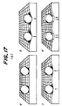
- a polaron is a freely moving conduction electron or a positive hole associated with LO-phonons or latice deformations or even more generally with electronic polarization as schematically illustrated in Fig. 17(a).
- Fig. 17(b) There is also even a concept of "bipolaron" due to coherent electronphonon intraction or electron-electron correlation effects as illustrated in Fig. 17(b).
- An exciton is an entity of elementary excitation as depicted in Fig. 18(a) which consists of a conduction electron and a positive hole bound together in an atomic hydrogen-like manner, sometimes, hybridized with (b) phonons to compose a "polariton".
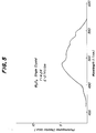
- the spectral response or photoresponse signal Q(T, ⁇ ) of the curves (a) and (b) of Fig. 2 implies that there exist such parts in the specimen of Ca 2-x -Sr x -Bi 3-y -Cu y -O z system oxide which are similar to Bi2O3 in an atomic sense, e.g., the (Bi2O2)+ layer.
- the phenomena of optical absorption and photoconductivity of Bi2O3 have been clarified even only in part neither by experiments nor by the exciton theory. However, it is probably a typical example of Frenkel type exciton that is related to and associated with mobile charge in cation shell.
- a superconductive optoelectronic device comprises a source region, a drain region, the two regions being made of superconductive material, and a gate region made of "superconductive photoconductive-material” revealing photoconductivity at a temperature below the transition temperature of the above superconductive material.
- the invention provides an optoelectronic device with intrinsic "superconductive properties", i.e., extremely low generation rate of heat such as Joule heat during operation, and it facilitates development of various novel superconducting devices such as “an optically controllable superconductive Josephson junction devices” and “superconductive phototransistors”.
- a two-dimensional alley-like device with a high density integration of the superconductive optoelectronic devices of the invention has such electrodes and lead wire terminals which are of perfect diamagnetism, so that it is free from noises and interferences due to mutual electromagentic induction between adjacent devices or due to outside magnetic fields. Therefore, the invention enables production of an ideal "superconductive optoelectronic device or apparatus" which operates under optimal thermal and electromagentic conditions, such as a space parallel optical computer with a very high operating speed.
- the present invention is a pioneer in novel scientific field of "Superconductive Opto-Electronics”.
Landscapes
- Superconductor Devices And Manufacturing Methods Thereof (AREA)
Claims (6)
- Dispositif optoélectronique supraconducteur comprenant un substrat (1), une région de grille photoconductrice (2) formée sur le substrat. et une région de source (3) et une région de drain (4) formées sur le substrat respectivement au niveau de côtés opposés de la région de grille de manière à être en face l'une de l'autre par rapport à la région de grille, et un moyen pour appliquer une tension de polarisation entre ladite région de source et ladite région de drain, lesdites régions de source et de drain étant réalisées en un matériau supraconducteur, ladite région de grille étant réalisée en un matériau à caractéristiques conjuguées de photoconduction et de supraconduction, c'est-à-dire un matériau présentant la même formule chimique générale que le matériau supraconducteur mais présentant des teneurs différentes en éléments constitutifs, lequel révèle une photoconductivité à une température inférieure à la température critique pour la supraconductivité dudit matériau supraconducteur et ainsi, un courant électrique qui circule entre ladite région de source et ladite région de drain est commandé en fonction de l'intensité de la lumière qui arrive en incidence sur la région de grille.
- Dispositif optoélectronique supraconducteur selon la revendication 1, dans lequel la région de grille photoconductrice est réalisée en un matériau à caractéristiques conjuguées de photoconduction et de supraconduction présentant la formule chimique générale Y3-x-Bax-Cuy-Oz dont les nombres d'atomes sont les suivants:
0≤x≤1, y=3, 7,0≤z≤7,5, et ladite région de source et ladite région de drain sont réalisées en un matériau supraconducteur présentant la formule chimique générale Y3-x-Bax-Cuy-Oz dont les nombres d'atomes sont les suivants:
1≤x≤2, y=3, 6,5≤z≤7. - Dispositif optoélectronique supraconducteur selon la revendication 1, dans lequel la région de grille photoconductrice est réalisée en un matériau à caractéristiques conjuguées de photoconduction et de supraconduction présentant la formule chimique générale Y3-x-Bax-Cuy-Oz dont les nombres d'atomes sont les suivants:
x=2, y=3, 6,0≤z≤6,5, et ladite région de source et ladite région de drain sont réalisées en un matériau supraconducteur présentant la formule chimique générale Y3-x-Bax-Cuy-Oz dont les nombres d'atomes sont les suivants:
1≤x≤2, y=3, 6,5≤z≤7. - Dispositif optoélectronique supraconducteur selon la revendication 1, dans lequel la région de grille photoconductrice est réalisée en un matériau à caractéristiques conjuguées de photoconduction et de supraconduction présentant la formule chimique générale La₂-Cu₁-Oz dont le nombre d'atomes est le suivant:
3,86≤z≤3,92, et ladite région de source et ladite région de drain sont réalisées en un matériau supraconducteur présentant la formule chimique générale La₂-Cu₁-Oz dont le nombre d'atomes est le suivant:
3,92<z≤4,02. - Dispositif optoélectronique supraconducteur selon la revendication 1. dans lequel la région de grille photoconductrice est réalisée en un matériau à caractéristiques conjuguées de photoconduction et de supraconduction présentant la formule chimique générale Cam-xSrx-Bin-y-Cuy-Oz dont les nombres d'atomes sont les suivants:
2≤m≤4, 0≤x≤2, 3≤n≤5, 1≤y≤3, 4≤z≤11, et ladite région de source et ladite région de drain sont réalisées en un matériau supraconducteur présentant la formule chimique générale Cam-x-Srx-Bin-y-Cuy-Oz dont les nombres d'atomes sont les suivants:
2≤m≤4, 1≤x≤2, 3≤n≤5, 1≤y≤3, 4≤z≤11. - Dispositif optoélectronique supraconducteur selon la revendication 1, dans lequel la région de grille photoconductrice est réalisée en un matériau à caractéristiques conjuguées de photoconduction et de supraconduction présentant la formule chimique générale Ba₁-Pb1-x-Bix-Oz dont les nombres d'atomes sont les suivants:
0,35≤x, 2,7≤z≤3, et ladite région de source et ladite région de drain sont réalisées en un matériau supraconducteur présentant la formule chimique générale Ba₁-Pb1-x-Bix-Oz dont les nombres d'atomes sont les suivants:
0,2≤x≤0,35, 2,81≤z≤3.
Applications Claiming Priority (4)
| Application Number | Priority Date | Filing Date | Title |
|---|---|---|---|
| JP57844/88 | 1988-03-11 | ||
| JP5784488 | 1988-03-11 | ||
| JP201655/88 | 1988-08-12 | ||
| JP63201655A JPH01315177A (ja) | 1988-03-11 | 1988-08-12 | 超伝導オプトエレクトロニクス素子及び超伝導オプトエレクトロニクス装置 |
Publications (3)
| Publication Number | Publication Date |
|---|---|
| EP0332448A2 EP0332448A2 (fr) | 1989-09-13 |
| EP0332448A3 EP0332448A3 (en) | 1989-11-23 |
| EP0332448B1 true EP0332448B1 (fr) | 1996-05-15 |
Family
ID=26398929
Family Applications (1)
| Application Number | Title | Priority Date | Filing Date |
|---|---|---|---|
| EP89302357A Expired - Lifetime EP0332448B1 (fr) | 1988-03-11 | 1989-03-09 | Dispositif de supraconducteurs opto-électroniques |
Country Status (4)
| Country | Link |
|---|---|
| US (1) | US4990487A (fr) |
| EP (1) | EP0332448B1 (fr) |
| CA (1) | CA1310391C (fr) |
| DE (1) | DE68926471T2 (fr) |
Families Citing this family (31)
| Publication number | Priority date | Publication date | Assignee | Title |
|---|---|---|---|---|
| US5168165A (en) * | 1988-02-04 | 1992-12-01 | The University Of Tokyo | Superconductive photoconductive-substance of the Y-Ba-Cu-O system and a method for producing the same |
| US5219831A (en) * | 1988-02-04 | 1993-06-15 | University Of Tokyo | Superconductive photoconductive-substance of the La-Cu-O system and a method for producing the same |
| JPH06102548B2 (ja) * | 1988-08-12 | 1994-12-14 | 東京大学長 | Ba−Pb−Bi−O系酸化物超伝導性光伝導物質及びその製造法 |
| JPH06102549B2 (ja) * | 1988-08-12 | 1994-12-14 | 東京大学長 | Ca−Sr−Bi−Cu−O系酸化物超伝導性光伝導物質及びその製造法 |
| EP0407166B1 (fr) * | 1989-07-05 | 1994-05-25 | Canon Kabushiki Kaisha | Appareil et procédé pour la détection de lumière |
| JP2503091B2 (ja) * | 1990-03-14 | 1996-06-05 | 富士通株式会社 | 超電導光機能素子 |
| JPH065791B2 (ja) * | 1990-05-11 | 1994-01-19 | 東京大学長 | 超伝導性光伝導基本物質Cu2O系材料を用いた超伝導オプトエレクトロニクス装置 |
| JPH065792B2 (ja) * | 1990-08-03 | 1994-01-19 | 東京大学長 | 超伝導性光伝導基本物質Bi▲下2▼0▲下3▼系材料を用いた超伝導オプトエレクトロニクス装置 |
| US5116807A (en) * | 1990-09-25 | 1992-05-26 | The United States Of America As Represented By The Administrator Of The National Aeronautics And Space Administration | Monolithic MM-wave phase shifter using optically activated superconducting switches |
| US5328893A (en) * | 1991-06-24 | 1994-07-12 | Superconductor Technologies, Inc. | Superconducting devices having a variable conductivity device for introducing energy loss |
| JPH07109905B2 (ja) * | 1991-07-16 | 1995-11-22 | 東京大学長 | Bi−SrCa(LaY)−Cu−O系酸化物超伝導共役性光伝導物質及びその製造法並びにこれを用いた超伝導オプトエレクトロニクス装置 |
| US5768002A (en) * | 1996-05-06 | 1998-06-16 | Puzey; Kenneth A. | Light modulation system including a superconductive plate assembly for use in a data transmission scheme and method |
| JP3511098B2 (ja) * | 2001-09-14 | 2004-03-29 | 独立行政法人産業技術総合研究所 | 超高速光電気信号変換素子 |
| DE102005018835A1 (de) | 2005-04-22 | 2006-11-02 | Degussa Ag | Verfahren zur Herstellung von L-Aminosäuren unter Verwendung verbesserter Stämme der Familie Enterobacteriaceae |
| US20100013559A1 (en) * | 2007-02-02 | 2010-01-21 | Max Lee B | High frequency amplifying device |
| DE102007051024A1 (de) | 2007-03-05 | 2008-09-11 | Evonik Degussa Gmbh | Verfahren zur Herstellung von L-Aminosäuren unter Verwendung von Stämmen der Familie Enterobacteriaceae |
| EP1975241A1 (fr) | 2007-03-29 | 2008-10-01 | Evonik Degussa GmbH | Procédé de fabrication d'aminoacides L en utilisant des troncs améliorés de la famille des enterobacteriaceae |
| DE102007044134A1 (de) | 2007-09-15 | 2009-03-19 | Evonik Degussa Gmbh | Verfahren zur Herstellung von L-Aminosäuren unter Verwendung von verbesserten Stämmen der Familie Enterobacteriaceae |
| DE102007052270A1 (de) | 2007-11-02 | 2009-05-07 | Evonik Degussa Gmbh | Verfahren zur Herstellung von L-Aminosäuren unter Verwendung von verbesserten Stämmen der Familie Enterobacteriaceae |
| EP2060636A1 (fr) | 2007-11-14 | 2009-05-20 | Evonik Degussa GmbH | Procédé de fabrication d'acides aminés L en utilisant des souches de la famille des Enterobacteriaceae améliorées |
| EP2098597A1 (fr) | 2008-03-04 | 2009-09-09 | Evonik Degussa GmbH | Procédé de fabrication d'aminoacides L en utilisant des troncs améliorés de la famille des enterobacteriaceae |
| DE102008002309A1 (de) | 2008-06-09 | 2009-12-10 | Evonik Degussa Gmbh | Verfahren zur Herstellung von L-Aminosäuren unter Verwendung von verbesserten Stämmen der Familie Enterobacteriaceae |
| DE102008040352A1 (de) | 2008-07-11 | 2010-01-14 | Evonik Degussa Gmbh | Verfahren zur Herstellung von L-Tryptophan unter Verwendung von verbesserten Stämmen der Familie Enterobacteriaceae |
| DE102008044768A1 (de) | 2008-08-28 | 2010-03-04 | Evonik Degussa Gmbh | Verfahren zur Herstellung von organisch-chemischen Verbindungen unter Verwendung von verbesserten Stämmen der Familie Enterobacteriaceae |
| EP2267145A1 (fr) | 2009-06-24 | 2010-12-29 | Evonik Degussa GmbH | Procédé de fabrication d'aminoacides L en utilisant des troncs améliorés de la famille des enterobacteriaceae |
| DE102009030342A1 (de) | 2009-06-25 | 2010-12-30 | Evonik Degussa Gmbh | Verfahren zur fermentativen Herstellung von organisch chemischen Verbindungen |
| DE102010003419B4 (de) | 2010-03-30 | 2019-09-12 | Evonik Degussa Gmbh | Verfahren zur fermentativen Herstellung von L-Ornithin |
| DE102011006716A1 (de) | 2011-04-04 | 2012-10-04 | Evonik Degussa Gmbh | Mikroorganismus und Verfahren zur fermentativen Herstellung einer organisch-chemischen Verbindung |
| EP2762571A1 (fr) | 2013-01-30 | 2014-08-06 | Evonik Industries AG | Microorganisme et procédé de fabrication par fermentation d'acides aminés |
| EP3608409A1 (fr) | 2018-08-09 | 2020-02-12 | Evonik Operations GmbH | Procédé de préparation d'acides aminés l au moyen de souches améliorées de la famille des enterobacteriaceae |
| DE102020213681A1 (de) | 2020-10-30 | 2022-05-05 | Forschungszentrum Jülich GmbH | Elektrolumineszenz keramischer Werkstoffe |
Family Cites Families (10)
| Publication number | Priority date | Publication date | Assignee | Title |
|---|---|---|---|---|
| NL286177A (fr) * | 1961-12-01 | |||
| US4464065A (en) * | 1982-08-09 | 1984-08-07 | The United States Of America As Represented By The Secretary Of The Navy | Fast granular superconducting bolometer |
| JPS6065582A (ja) * | 1983-09-20 | 1985-04-15 | Nippon Telegr & Teleph Corp <Ntt> | 粒界ジヨセフソン接合型光検出素子 |
| EP0147482B1 (fr) * | 1983-12-28 | 1987-08-19 | International Business Machines Corporation | Transistor tunnel pour basses températures |
| JPS60253929A (ja) * | 1984-05-31 | 1985-12-14 | Shimadzu Corp | 赤外線イメ−ジセンサ |
| JPS61271487A (ja) * | 1985-05-27 | 1986-12-01 | Masahiko Kurakado | 超伝導トンネル接合を用いた放射線および光入射位置検出器 |
| US4843446A (en) * | 1986-02-27 | 1989-06-27 | Hitachi, Ltd. | Superconducting photodetector |
| JPS63241809A (ja) * | 1987-03-27 | 1988-10-07 | Sumitomo Electric Ind Ltd | 透明導電体 |
| JPS63245973A (ja) * | 1987-03-31 | 1988-10-13 | Sumitomo Electric Ind Ltd | 超電導素子 |
| US4814598A (en) * | 1987-09-03 | 1989-03-21 | Hypres, Inc. | Optical wavelength analyzer and image processing system utilizing Josephson junctions |
-
1989
- 1989-03-07 US US07/320,131 patent/US4990487A/en not_active Expired - Lifetime
- 1989-03-08 CA CA000593077A patent/CA1310391C/fr not_active Expired - Lifetime
- 1989-03-09 DE DE68926471T patent/DE68926471T2/de not_active Expired - Fee Related
- 1989-03-09 EP EP89302357A patent/EP0332448B1/fr not_active Expired - Lifetime
Also Published As
| Publication number | Publication date |
|---|---|
| DE68926471D1 (de) | 1996-06-20 |
| DE68926471T2 (de) | 1996-11-28 |
| CA1310391C (fr) | 1992-11-17 |
| EP0332448A3 (en) | 1989-11-23 |
| EP0332448A2 (fr) | 1989-09-13 |
| US4990487A (en) | 1991-02-05 |
Similar Documents
| Publication | Publication Date | Title |
|---|---|---|
| EP0332448B1 (fr) | Dispositif de supraconducteurs opto-électroniques | |
| Wake et al. | Optically induced metastability in untwinned single-domain YBa 2 Cu 3 O 7 | |
| Loret et al. | Universal relationship between the energy scales of the pseudogap phase, the superconducting state, and the charge-density-wave order in copper oxide superconductors | |
| US5244870A (en) | Superconductive optoelectronic device with the basic substance Cu2 O of superconductive-conjugate photoconductivity | |
| Fisk et al. | The new generation high-temperature superconductors | |
| US5462916A (en) | Superconductive optoelectronic devices with the basic substance Bi2 O3 of superconductive-conjugate photoconductivity | |
| US5654259A (en) | Superconductive conjugate photoconductive substances of the Bi-SrCa (laY)-Cu-O system, a method for producing the same and superconductive optoelectronic devices using the same | |
| Chen et al. | Resistivity and thermoelectric power of Bi2Sr2Ca− xPrxCu2Oy system | |
| US5554584A (en) | Superconductive photoconductive substance of the Ca-Sr-Bi-Cu-O group system and a method of producing the same | |
| CA1338852C (fr) | Susbtance supraconductrice et photoconductrice du type lacuo et methode de fabrication de cette substance | |
| US5151409A (en) | Superconducting composition comprising ln-th-cu-o, wherein ln is pr, nd, pm, sm, eu, gd, er or mixtures thereof | |
| JPH01315177A (ja) | 超伝導オプトエレクトロニクス素子及び超伝導オプトエレクトロニクス装置 | |
| US5219831A (en) | Superconductive photoconductive-substance of the La-Cu-O system and a method for producing the same | |
| US5168165A (en) | Superconductive photoconductive-substance of the Y-Ba-Cu-O system and a method for producing the same | |
| US5371067A (en) | Superconductive photoconductive substance of the Ba-Pb-Bi-O group system and a method for producing the same | |
| Masumi | Photoconductivity with anomalies in insulators correlated with high-Tc superconductivity | |
| US5140002A (en) | Photoconductive-substance of the Y-Ba-Cu-O system and a method for producing the same | |
| CA1338851C (fr) | Substance supraconductrice et photoconductrice du type ybacuo et methode de fabrication de cette substance | |
| THOMPSON et al. | NORMAL STATE PROPERTIES OF CU-O SUPERCONDUCTORS | |
| Hayashi et al. | Characteristics of Superconducting Gd-Ba-Cu-O Thin Films | |
| Chuang et al. | Constancy of the bilayer splitting as a function of doping in $ Bi_ {2} Sr_ {2} CaCu_ {2} O_ {8+\delta} $ |
Legal Events
| Date | Code | Title | Description |
|---|---|---|---|
| PUAI | Public reference made under article 153(3) epc to a published international application that has entered the european phase |
Free format text: ORIGINAL CODE: 0009012 |
|
| AK | Designated contracting states |
Kind code of ref document: A2 Designated state(s): BE CH DE FR GB IT LI NL |
|
| PUAL | Search report despatched |
Free format text: ORIGINAL CODE: 0009013 |
|
| AK | Designated contracting states |
Kind code of ref document: A3 Designated state(s): BE CH DE FR GB IT LI NL |
|
| 17P | Request for examination filed |
Effective date: 19900522 |
|
| 17Q | First examination report despatched |
Effective date: 19930222 |
|
| GRAH | Despatch of communication of intention to grant a patent |
Free format text: ORIGINAL CODE: EPIDOS IGRA |
|
| GRAA | (expected) grant |
Free format text: ORIGINAL CODE: 0009210 |
|
| AK | Designated contracting states |
Kind code of ref document: B1 Designated state(s): BE CH DE FR GB IT LI NL |
|
| ITF | It: translation for a ep patent filed | ||
| REF | Corresponds to: |
Ref document number: 68926471 Country of ref document: DE Date of ref document: 19960620 |
|
| REG | Reference to a national code |
Ref country code: CH Ref legal event code: NV Representative=s name: KIRKER & CIE SA |
|
| ET | Fr: translation filed | ||
| PLBE | No opposition filed within time limit |
Free format text: ORIGINAL CODE: 0009261 |
|
| STAA | Information on the status of an ep patent application or granted ep patent |
Free format text: STATUS: NO OPPOSITION FILED WITHIN TIME LIMIT |
|
| REG | Reference to a national code |
Ref country code: CH Ref legal event code: NV Representative=s name: RITSCHER & SEIFERT PATENTANWAELTE VSP |
|
| 26N | No opposition filed | ||
| REG | Reference to a national code |
Ref country code: GB Ref legal event code: IF02 |
|
| PGFP | Annual fee paid to national office [announced via postgrant information from national office to epo] |
Ref country code: GB Payment date: 20040303 Year of fee payment: 16 |
|
| PGFP | Annual fee paid to national office [announced via postgrant information from national office to epo] |
Ref country code: FR Payment date: 20040309 Year of fee payment: 16 |
|
| PGFP | Annual fee paid to national office [announced via postgrant information from national office to epo] |
Ref country code: NL Payment date: 20040310 Year of fee payment: 16 |
|
| PGFP | Annual fee paid to national office [announced via postgrant information from national office to epo] |
Ref country code: CH Payment date: 20040317 Year of fee payment: 16 |
|
| PGFP | Annual fee paid to national office [announced via postgrant information from national office to epo] |
Ref country code: DE Payment date: 20040318 Year of fee payment: 16 |
|
| PGFP | Annual fee paid to national office [announced via postgrant information from national office to epo] |
Ref country code: BE Payment date: 20040518 Year of fee payment: 16 |
|
| PG25 | Lapsed in a contracting state [announced via postgrant information from national office to epo] |
Ref country code: IT Free format text: LAPSE BECAUSE OF NON-PAYMENT OF DUE FEES;WARNING: LAPSES OF ITALIAN PATENTS WITH EFFECTIVE DATE BEFORE 2007 MAY HAVE OCCURRED AT ANY TIME BEFORE 2007. THE CORRECT EFFECTIVE DATE MAY BE DIFFERENT FROM THE ONE RECORDED. Effective date: 20050309 Ref country code: GB Free format text: LAPSE BECAUSE OF NON-PAYMENT OF DUE FEES Effective date: 20050309 |
|
| PG25 | Lapsed in a contracting state [announced via postgrant information from national office to epo] |
Ref country code: LI Free format text: LAPSE BECAUSE OF NON-PAYMENT OF DUE FEES Effective date: 20050331 Ref country code: CH Free format text: LAPSE BECAUSE OF NON-PAYMENT OF DUE FEES Effective date: 20050331 Ref country code: BE Free format text: LAPSE BECAUSE OF NON-PAYMENT OF DUE FEES Effective date: 20050331 |
|
| BERE | Be: lapsed |
Owner name: THE *UNIVERSITY OF TOKYO Effective date: 20050331 |
|
| PG25 | Lapsed in a contracting state [announced via postgrant information from national office to epo] |
Ref country code: NL Free format text: LAPSE BECAUSE OF NON-PAYMENT OF DUE FEES Effective date: 20051001 Ref country code: DE Free format text: LAPSE BECAUSE OF NON-PAYMENT OF DUE FEES Effective date: 20051001 |
|
| REG | Reference to a national code |
Ref country code: CH Ref legal event code: PL |
|
| GBPC | Gb: european patent ceased through non-payment of renewal fee |
Effective date: 20050309 |
|
| PG25 | Lapsed in a contracting state [announced via postgrant information from national office to epo] |
Ref country code: FR Free format text: LAPSE BECAUSE OF NON-PAYMENT OF DUE FEES Effective date: 20051130 |
|
| NLV4 | Nl: lapsed or anulled due to non-payment of the annual fee |
Effective date: 20051001 |
|
| REG | Reference to a national code |
Ref country code: FR Ref legal event code: ST Effective date: 20051130 |
|
| BERE | Be: lapsed |
Owner name: THE *UNIVERSITY OF TOKYO Effective date: 20050331 |