EP0332972A1 - Méthod et dispositif pour transfert de données - Google Patents
Méthod et dispositif pour transfert de données Download PDFInfo
- Publication number
- EP0332972A1 EP0332972A1 EP89103912A EP89103912A EP0332972A1 EP 0332972 A1 EP0332972 A1 EP 0332972A1 EP 89103912 A EP89103912 A EP 89103912A EP 89103912 A EP89103912 A EP 89103912A EP 0332972 A1 EP0332972 A1 EP 0332972A1
- Authority
- EP
- European Patent Office
- Prior art keywords
- memory
- data
- bus
- channels
- address
- Prior art date
- Legal status (The legal status is an assumption and is not a legal conclusion. Google has not performed a legal analysis and makes no representation as to the accuracy of the status listed.)
- Granted
Links
Images


Classifications
-
- G—PHYSICS
- G06—COMPUTING OR CALCULATING; COUNTING
- G06F—ELECTRIC DIGITAL DATA PROCESSING
- G06F13/00—Interconnection of, or transfer of information or other signals between, memories, input/output devices or central processing units
- G06F13/38—Information transfer, e.g. on bus
-
- G—PHYSICS
- G06—COMPUTING OR CALCULATING; COUNTING
- G06F—ELECTRIC DIGITAL DATA PROCESSING
- G06F13/00—Interconnection of, or transfer of information or other signals between, memories, input/output devices or central processing units
- G06F13/38—Information transfer, e.g. on bus
- G06F13/40—Bus structure
- G06F13/4004—Coupling between buses
- G06F13/4027—Coupling between buses using bus bridges
- G06F13/405—Coupling between buses using bus bridges where the bridge performs a synchronising function
- G06F13/4054—Coupling between buses using bus bridges where the bridge performs a synchronising function where the function is bus cycle extension, e.g. to meet the timing requirements of the target bus
-
- G—PHYSICS
- G06—COMPUTING OR CALCULATING; COUNTING
- G06F—ELECTRIC DIGITAL DATA PROCESSING
- G06F5/00—Methods or arrangements for data conversion without changing the order or content of the data handled
- G06F5/06—Methods or arrangements for data conversion without changing the order or content of the data handled for changing the speed of data flow, i.e. speed regularising or timing, e.g. delay lines, FIFO buffers; over- or underrun control therefor
- G06F5/065—Partitioned buffers, e.g. allowing multiple independent queues, bidirectional FIFO's
Definitions
- the invention relates to a method for data transmission and an arrangement for carrying out the method according to the preambles of claims 1 and 7.
- the data transmitter or data receiver is, for example, a processor which is connected to slower-working peripheral units via a fast processor bus.
- One example is a data acquisition system in which data that is generated quickly must first be temporarily stored in order to then be sent for further processing via the fast processor bus. In all cases, data is generated at a higher speed than can be further processed, so that certain data quantities must first be buffered.
- fast memories known as caches, for these amounts of data. These caches are usually built from ECL memories, for which a parallelization of storage units is not necessary. However, the sizes of the caches are severely limited by ECL memory.
- a data acquisition system is described below, by way of example, in which external data are recorded at a higher speed than they can be further processed. Examples of these applications are fast digital storage oscilloscopes, transient recorders or high-resolution image acquisition systems.
- the data is temporarily stored in a memory with parallelization (cache) and then fed to a processor system.
- the parallelization and storage of the data obtained via a serial data path at high speed can be done with the aid of demultiplexer modules, e.g. a data acquisition shift register. It is expressly pointed out that the invention described below is not applicable to data acquisition systems, but rather in the same way to data transmission systems in which data is transmitted via a fast processor bus, is temporarily stored and then processed in peripheral units.
- a fast, n-bit wide, serial data path results in data which are divided into N-parallel channels of a memory with the aid of demultiplexers. If the number N of parallel channels is 12, for example, then slow memories with optional access, for example static CMOS RAMs with a typical access time of 100 ns, can be used in the memory (cache).
- the data is then to be transferred via a fast processor bus, which consists of a control bus, an address bus and a data bus, into a system memory, which usually consists of dynamic random access memories (DRAM).
- DRAM dynamic random access memories
- the data transmission is controlled by a control device, for example a data acquisition controller (DACO), which generates the address and control lines for the memories and the selection signals for the channels.
- the individual memory channels are closed orderly controllable connecting links connected to the data bus.
- the controllable connecting links are, for example, bus drivers with three control states (tristate bus drivers).
- the data to be stored which is supplied serially by a fast A / D converter, for example, can be written continuously to the individual channels or memory addresses of the memory, and then for each memory address with the aid of the selection signals, the memory channel and the Associated bus drivers can be controlled in order to transfer the data into the data bus of the bus system.
- the control device must work in such a way that the fastest possible transfer between the memory and the processor is achieved. It is known to provide direct memory access (DMA) for this, i.e. the control device must continuously address channels or memory addresses of the memory during the transmission in order to enable the data receiver, e.g. to offer the processor a continuous flow of data. In this case, the entire data acquisition system represents a peripheral input device for the processor. It is also known to provide the transfer of the channels of the memory in a bus cycle (single cycle transfer) in order to accelerate the transfer. The reading and writing process is carried out in one bus cycle. This option is available in particular if the data to be transferred do not have to be checked or modified during the transfer.
- DMA direct memory access
- the invention has for its object to reduce the number of waiting states required in a data transmission method and an arrangement of the type described and thus to increase the data transmission speed.
- the invention has the advantage that the access time of the memory or the memory channels must be taken into account only when reading out each new address or when writing into each new address, and that the reading out of the other channels from the line memory can be carried out quickly and without waiting states .
- the control device only has the task of inserting the required number of waiting states in each bus cycle after an address change (dynamic) by controlling the corresponding ready signal.
- the number of waiting states required is therefore reduced according to the invention in accordance with the reciprocal number of channels in the memory.
- Embodiments of the inventive concept are characterized in the subclaims.
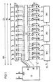
- the outputs of the controllable connecting elements SV and SVi are connected to the data bus DB of a bus BUS, which also includes an address bus AB and a control bus CB.
- a control device SE To control the data transmission between the channels of the memory SP and a data receiver, not shown, connected to the bus BUS, a control device SE is provided, which is connected via lines PI to the data receiver or to a processor via an interface. Furthermore, address outputs Adr of the control device are connected via k-bit wide address lines to the memory channels K0 to K11 of the memory SP or to corresponding address decoders.
- Another output of the control device SE is provided for the activation of the channels of the memory SP.
- this output is simultaneously connected via a common activation line to the channels K0 to K11 via which the signal ME (Memory Enable) can be transferred.
- Each of the controllable connecting links SV0 to SV11 is connected via an assigned connecting line to selection channels AK of the control device, via which selection signals can be transmitted.
- the controllable connecting links are preferably bus drivers with three controllable states.
- a standby signal BS is generated by a dynamic generator DGEN of the control device SE, with the aid of which wait states can be inserted into the bus cycle.
- this intermediate memory ZSP is provided between the channels K0 to K11 of the memory SP and the controllable connecting elements SV0 to SV11 of the tristate bus driver SV.
- the number of required waiting states can be reduced with the help of this buffer ZSP and a dynamic generator DGEN in the control device for generating the ready signal BS. Since all channels of the memory SP must be addressed in turn for each memory address, the data of all channels can be immediately transferred to the line memory ZSP after each change of the memory address. Only when each new address is read out for the first time must the access time of the memory channels or the memory SP be taken into account. The data of the other channels can be read out of the line memory quickly and therefore without waiting states.
- each bus cycle BZ the individual channels K0 to K11 or 0 to 11 of the memory SP are addressed in succession.
- a number of waiting states are inserted which correspond to m clock periods. These waiting states take into account the access time of the memory channel. No further waiting states need to be inserted for the further memory channels, since the memory SP is activated simultaneously on all channels with each change of address and the data to be transferred are merely temporarily stored in the intermediate memory ZSP.
- data transmission in the reverse direction i.e. a data transmission system with data writing from the data bus DB is shown the channels of the memory SP.
- a physical buffer is present in a data transmission system, which is implemented by memory elements of the controllable connecting links and is expressed by the reference symbol SVS or channel-by-channel SVS0 to SVS11.
- SVS reference symbol
- SVS channel-by-channel SVS0 to SVS11
- Tristate bus latches are preferred for the controllable connecting elements with memory elements.
- the transmission in a system according to FIG. 3 is explained in more detail using the data diagram according to FIG. 4.
- the access time of the memory channel must be taken into account during the transmission of the last channel before each change of the memory address in such a way that in the bus cycle BZ a corresponding number of waiting states WZ, namely, for example, m clock periods inserted will.
- the waiting states must therefore be inserted before each change in the memory address of the memory SP and not, as in data acquisition systems, directly after each change in the memory address.
- FIG. 5 shows an exemplary embodiment for the implementation of the dynamic generator DGEN for generating the ready signal BS.
- the number of required waiting states WZ is stored in a programmable counter PZ which is controlled by the system clock C.
- a pulse shaper stage PF is required for the time control within a bus cycle, which must be carried out specifically for the respective processor system.
- the execution of the respective pulse shaper stage is subject to the skill of an average specialist and belongs to the state of the art.
- the pulse shaper stage PF is controlled by the bus cycle BZ and the system clock C and makes the ready signal BS available for all bus cycles.
- a "bus cycle selection signal BZAS" signal is activated. This signal causes the interruption of the ready signal BS in the pulse shaper stage and at the same time with the aid of an AND gate A1, the second input of which is controlled by the pulse shaper stage PF and which emits a start signal ST for the start of the programmable counter PZ and thus the insertion of the corresponding m Clock cycles in the ready signal BS by the pulse shaper.
- the programmable counter PZ sends an end signal ES to the pulse shaper stage PF, which then generates the ready signal BS again, so that the bus cycle can be ended properly.
Landscapes
- Engineering & Computer Science (AREA)
- Theoretical Computer Science (AREA)
- General Engineering & Computer Science (AREA)
- Physics & Mathematics (AREA)
- General Physics & Mathematics (AREA)
- Computer Hardware Design (AREA)
- Information Transfer Systems (AREA)
- Small-Scale Networks (AREA)
- Bus Control (AREA)
- Image Input (AREA)
- Communication Control (AREA)
Priority Applications (1)
| Application Number | Priority Date | Filing Date | Title |
|---|---|---|---|
| AT89103912T ATE76697T1 (de) | 1988-03-15 | 1989-03-06 | Verfahren zur datenuebertragung und anordnung zur durchfuehrung des verfahrens. |
Applications Claiming Priority (2)
| Application Number | Priority Date | Filing Date | Title |
|---|---|---|---|
| DE3808640 | 1988-03-15 | ||
| DE3808640 | 1988-03-15 |
Publications (2)
| Publication Number | Publication Date |
|---|---|
| EP0332972A1 true EP0332972A1 (fr) | 1989-09-20 |
| EP0332972B1 EP0332972B1 (fr) | 1992-05-27 |
Family
ID=6349790
Family Applications (1)
| Application Number | Title | Priority Date | Filing Date |
|---|---|---|---|
| EP89103912A Expired - Lifetime EP0332972B1 (fr) | 1988-03-15 | 1989-03-06 | Méthod et dispositif pour transfert de données |
Country Status (5)
| Country | Link |
|---|---|
| EP (1) | EP0332972B1 (fr) |
| JP (1) | JPH01271862A (fr) |
| KR (1) | KR890015533A (fr) |
| AT (1) | ATE76697T1 (fr) |
| DE (1) | DE58901516D1 (fr) |
Families Citing this family (1)
| Publication number | Priority date | Publication date | Assignee | Title |
|---|---|---|---|---|
| JP5350677B2 (ja) * | 2008-05-19 | 2013-11-27 | 株式会社東芝 | バス信号制御回路、及び、バス信号制御回路を備えた信号処理回路 |
Citations (4)
| Publication number | Priority date | Publication date | Assignee | Title |
|---|---|---|---|---|
| DE2027567A1 (de) * | 1970-06-04 | 1971-12-09 | Siemens Ag | Speicher zur Zwischenspeicherung von Daten |
| US3789366A (en) * | 1969-04-18 | 1974-01-29 | Takachiho Koeki Kk | Random-access memory device using sequential-access memories |
| US4005389A (en) * | 1973-09-21 | 1977-01-25 | Siemens Aktiengesellschaft | Arrangement for reducing the access time in a storage system |
| FR2582423A1 (fr) * | 1985-05-22 | 1986-11-28 | Grenoble Inst Nal Polytechni | Memoire tampon a interposer entre deux systemes synchrones a vitesses differentes |
-
1989
- 1989-03-06 DE DE8989103912T patent/DE58901516D1/de not_active Expired - Lifetime
- 1989-03-06 EP EP89103912A patent/EP0332972B1/fr not_active Expired - Lifetime
- 1989-03-06 AT AT89103912T patent/ATE76697T1/de active
- 1989-03-13 JP JP1061981A patent/JPH01271862A/ja active Pending
- 1989-03-15 KR KR1019890003197A patent/KR890015533A/ko not_active Ceased
Patent Citations (4)
| Publication number | Priority date | Publication date | Assignee | Title |
|---|---|---|---|---|
| US3789366A (en) * | 1969-04-18 | 1974-01-29 | Takachiho Koeki Kk | Random-access memory device using sequential-access memories |
| DE2027567A1 (de) * | 1970-06-04 | 1971-12-09 | Siemens Ag | Speicher zur Zwischenspeicherung von Daten |
| US4005389A (en) * | 1973-09-21 | 1977-01-25 | Siemens Aktiengesellschaft | Arrangement for reducing the access time in a storage system |
| FR2582423A1 (fr) * | 1985-05-22 | 1986-11-28 | Grenoble Inst Nal Polytechni | Memoire tampon a interposer entre deux systemes synchrones a vitesses differentes |
Non-Patent Citations (1)
| Title |
|---|
| COMPUTER DESIGN, Band 21, Nr. 1, Januar 1982, Seiten 155-164, Winchester, Massachusetts, US; J.P. ALTNETHER: "Better processor performance via global memory" * |
Also Published As
| Publication number | Publication date |
|---|---|
| KR890015533A (ko) | 1989-10-30 |
| EP0332972B1 (fr) | 1992-05-27 |
| DE58901516D1 (de) | 1992-07-02 |
| ATE76697T1 (de) | 1992-06-15 |
| JPH01271862A (ja) | 1989-10-30 |
Similar Documents
| Publication | Publication Date | Title |
|---|---|---|
| DE3586245T2 (de) | Bildverarbeitungsgeraet und interkommunikationsbus dafuer. | |
| DE3232600C2 (fr) | ||
| DE69033482T2 (de) | Steuerungssystem für Systembus | |
| DE2703578A1 (de) | Videospeicher | |
| EP0848520A1 (fr) | Système de bus et méthode pour la transmission de données | |
| DE69130932T2 (de) | Speichersystem | |
| DE2854782C2 (de) | Datenverarbeitungssystem und Verfahren zum Ersetzen eines Datenblocks in einem Schnellspeicher | |
| DE2432608A1 (de) | Speicheranordnung fuer datenverarbeitungseinrichtungen | |
| DE68916945T2 (de) | Synchronisierschaltung für Datenüberträge zwischen zwei mit unterschiedlicher Geschwindigkeit arbeitenden Geräten. | |
| DE2456540C2 (de) | Inkrementalwertkodierer | |
| EP0380509A1 (fr) | Procede et dispositif de mesure pour l'analyse de perturbations de bus digitaux. | |
| DE3923872A1 (de) | Schaltungsanordnung zum steuern des zugriffs auf einen speicher | |
| EP0332972B1 (fr) | Méthod et dispositif pour transfert de données | |
| EP0694843B1 (fr) | Procédé et dispositif de commande d'une séquence d'accès de processeur à une mémoire associée | |
| DE3644322C2 (fr) | ||
| DE69321544T2 (de) | Halbleiterspeicheranordnung | |
| DE602004005806T2 (de) | Serieller Speicher mit Mitteln zur Integration eines erweiterten Speicherfeldes | |
| DE2404887A1 (de) | Kanal fuer den informationsaustausch zwischen einem rechner und schnellen peripheren einheiten | |
| DE3587635T2 (de) | Plattenspeichersteuergerät mit geteiltem Adressenregister. | |
| DE10157874B4 (de) | Vorrichtung zum Zuführen von Steuersignalen zu Speichereinheiten und dafür angepasste Speichereinheit | |
| DE3009317A1 (de) | Hybrid-assoziativspeicher | |
| EP0301160A2 (fr) | Système à deux microprocesseurs et mémoire écriture/lecture partagée | |
| DE2630711A1 (de) | Speichersteuersystem | |
| DE2837709C2 (de) | Schaltungsanordnung zur Behandlung von Teilwörtern in Rechnersystemen | |
| DE10159180A1 (de) | Speichervorrichtung und Verfahren zum Speichern und zum Auslesen von Datenströmen |
Legal Events
| Date | Code | Title | Description |
|---|---|---|---|
| PUAI | Public reference made under article 153(3) epc to a published international application that has entered the european phase |
Free format text: ORIGINAL CODE: 0009012 |
|
| AK | Designated contracting states |
Kind code of ref document: A1 Designated state(s): AT BE CH DE FR GB IT LI LU NL SE |
|
| 17P | Request for examination filed |
Effective date: 19891010 |
|
| 17Q | First examination report despatched |
Effective date: 19910304 |
|
| GRAA | (expected) grant |
Free format text: ORIGINAL CODE: 0009210 |
|
| AK | Designated contracting states |
Kind code of ref document: B1 Designated state(s): AT BE CH DE FR GB IT LI LU NL SE |
|
| REF | Corresponds to: |
Ref document number: 76697 Country of ref document: AT Date of ref document: 19920615 Kind code of ref document: T |
|
| REF | Corresponds to: |
Ref document number: 58901516 Country of ref document: DE Date of ref document: 19920702 |
|
| ET | Fr: translation filed | ||
| ITF | It: translation for a ep patent filed | ||
| GBT | Gb: translation of ep patent filed (gb section 77(6)(a)/1977) | ||
| PLBE | No opposition filed within time limit |
Free format text: ORIGINAL CODE: 0009261 |
|
| STAA | Information on the status of an ep patent application or granted ep patent |
Free format text: STATUS: NO OPPOSITION FILED WITHIN TIME LIMIT |
|
| 26N | No opposition filed | ||
| EPTA | Lu: last paid annual fee | ||
| PGFP | Annual fee paid to national office [announced via postgrant information from national office to epo] |
Ref country code: CH Payment date: 19940617 Year of fee payment: 6 |
|
| EAL | Se: european patent in force in sweden |
Ref document number: 89103912.5 |
|
| PGFP | Annual fee paid to national office [announced via postgrant information from national office to epo] |
Ref country code: LU Payment date: 19950301 Year of fee payment: 7 |
|
| PGFP | Annual fee paid to national office [announced via postgrant information from national office to epo] |
Ref country code: BE Payment date: 19950315 Year of fee payment: 7 |
|
| PGFP | Annual fee paid to national office [announced via postgrant information from national office to epo] |
Ref country code: SE Payment date: 19950330 Year of fee payment: 7 |
|
| PG25 | Lapsed in a contracting state [announced via postgrant information from national office to epo] |
Ref country code: LI Effective date: 19950331 Ref country code: CH Effective date: 19950331 |
|
| REG | Reference to a national code |
Ref country code: CH Ref legal event code: PL |
|
| PGFP | Annual fee paid to national office [announced via postgrant information from national office to epo] |
Ref country code: GB Payment date: 19960220 Year of fee payment: 8 |
|
| PGFP | Annual fee paid to national office [announced via postgrant information from national office to epo] |
Ref country code: AT Payment date: 19960223 Year of fee payment: 8 |
|
| PG25 | Lapsed in a contracting state [announced via postgrant information from national office to epo] |
Ref country code: LU Free format text: LAPSE BECAUSE OF NON-PAYMENT OF DUE FEES Effective date: 19960306 |
|
| PG25 | Lapsed in a contracting state [announced via postgrant information from national office to epo] |
Ref country code: SE Effective date: 19960307 |
|
| PGFP | Annual fee paid to national office [announced via postgrant information from national office to epo] |
Ref country code: NL Payment date: 19960328 Year of fee payment: 8 Ref country code: FR Payment date: 19960328 Year of fee payment: 8 |
|
| PG25 | Lapsed in a contracting state [announced via postgrant information from national office to epo] |
Ref country code: BE Effective date: 19960331 |
|
| PGFP | Annual fee paid to national office [announced via postgrant information from national office to epo] |
Ref country code: DE Payment date: 19960520 Year of fee payment: 8 |
|
| BERE | Be: lapsed |
Owner name: SIEMENS A.G. Effective date: 19960331 |
|
| EUG | Se: european patent has lapsed |
Ref document number: 89103912.5 |
|
| PG25 | Lapsed in a contracting state [announced via postgrant information from national office to epo] |
Ref country code: GB Effective date: 19970306 Ref country code: AT Effective date: 19970306 |
|
| PG25 | Lapsed in a contracting state [announced via postgrant information from national office to epo] |
Ref country code: NL Effective date: 19971001 |
|
| GBPC | Gb: european patent ceased through non-payment of renewal fee |
Effective date: 19970306 |
|
| PG25 | Lapsed in a contracting state [announced via postgrant information from national office to epo] |
Ref country code: FR Free format text: LAPSE BECAUSE OF NON-PAYMENT OF DUE FEES Effective date: 19971128 |
|
| NLV4 | Nl: lapsed or anulled due to non-payment of the annual fee |
Effective date: 19971001 |
|
| PG25 | Lapsed in a contracting state [announced via postgrant information from national office to epo] |
Ref country code: DE Effective date: 19971202 |
|
| REG | Reference to a national code |
Ref country code: FR Ref legal event code: ST |
|
| PG25 | Lapsed in a contracting state [announced via postgrant information from national office to epo] |
Ref country code: IT Free format text: LAPSE BECAUSE OF NON-PAYMENT OF DUE FEES;WARNING: LAPSES OF ITALIAN PATENTS WITH EFFECTIVE DATE BEFORE 2007 MAY HAVE OCCURRED AT ANY TIME BEFORE 2007. THE CORRECT EFFECTIVE DATE MAY BE DIFFERENT FROM THE ONE RECORDED. Effective date: 20050306 |