EP0694843B1 - Procédé et dispositif de commande d'une séquence d'accès de processeur à une mémoire associée - Google Patents
Procédé et dispositif de commande d'une séquence d'accès de processeur à une mémoire associée Download PDFInfo
- Publication number
- EP0694843B1 EP0694843B1 EP95111343A EP95111343A EP0694843B1 EP 0694843 B1 EP0694843 B1 EP 0694843B1 EP 95111343 A EP95111343 A EP 95111343A EP 95111343 A EP95111343 A EP 95111343A EP 0694843 B1 EP0694843 B1 EP 0694843B1
- Authority
- EP
- European Patent Office
- Prior art keywords
- memory
- processor
- address
- sram
- access
- Prior art date
- Legal status (The legal status is an assumption and is not a legal conclusion. Google has not performed a legal analysis and makes no representation as to the accuracy of the status listed.)
- Expired - Lifetime
Links
Images

Classifications
-
- G—PHYSICS
- G06—COMPUTING OR CALCULATING; COUNTING
- G06F—ELECTRIC DIGITAL DATA PROCESSING
- G06F12/00—Accessing, addressing or allocating within memory systems or architectures
- G06F12/02—Addressing or allocation; Relocation
- G06F12/06—Addressing a physical block of locations, e.g. base addressing, module addressing, memory dedication
- G06F12/0607—Interleaved addressing
-
- G—PHYSICS
- G06—COMPUTING OR CALCULATING; COUNTING
- G06F—ELECTRIC DIGITAL DATA PROCESSING
- G06F12/00—Accessing, addressing or allocating within memory systems or architectures
- G06F12/02—Addressing or allocation; Relocation
- G06F12/08—Addressing or allocation; Relocation in hierarchically structured memory systems, e.g. virtual memory systems
- G06F12/0802—Addressing of a memory level in which the access to the desired data or data block requires associative addressing means, e.g. caches
- G06F12/0877—Cache access modes
- G06F12/0879—Burst mode
Definitions
- the processing power of microprocessor systems depends on the one hand on the internal processing speed of the processor and others on the speed of access to a connected one Memory, especially working memory. Because the current Microprocessor systems, for example 486 DX from Intel, have very high internal processing speeds, is the processing power of the microprocessors in the essentially through the access times to the connected Memory limited. For the design of working memories for microprocessors, especially in communication systems, i.e. Telecommunications switching systems, so far dynamic RAM memory chips (DRAM) used, which a relatively small external cache memory is connected upstream. In A cache memory is the most common depending on the strategy or most recently used memory addresses and / or data saved. Such memory concepts are for personal computer applications beneficial and achieve an acceptable Processing power; a working memory concept with properties described below for communication systems however cannot be reached.
- DRAM dynamic RAM memory chips
- microprocessor systems with the known cache memories are in the majority of access cycles to the Memory wait cycles required to pass through not to fall short of the specified access time, as part of an access cycle in the microprocessor system be formed. This means a significant reduction the processing performance of especially modern ones Microprocessor systems, their internal processing speeds always increasing.
- the invention has for its object a method and an arrangement for controlling a sequence of accesses Processor to an allocated memory under Consideration of a particularly advantageous storage concept for communication systems in such a way that the processing performance especially when accessing the RAM is increased.
- the task is accomplished through a process with the features of claim 1 or by a Arrangement with the features of claim 6 solved.
- the method according to the invention is based on a division the memory to which the microprocessor has the shortest access times should access in at least two by static Memory banks implemented partial memories.
- Static Read / write memories have shorter access times dynamic read / write memories, which means that a subdivision of the memory in a few partial memories or memory banks processor-compatible, short memory access cycles can be achieved are.
- the memory sequence addresses immediately formed and attached to the partial store two partial stores on the other - controlled.
- the number of partial memories is dependent on the difference (n-m), the number of processor cycles of a read or write cycle running in the memory (SP) and the number m of processor cycles of one controlled via the processor bus (B) Access cycle to the memory determined - claim 2.
- dividing the memory into two partial memories is sufficient to achieve the maximum access speed to the partial memories controlled by the processor.
- the partial memories are addressed alternately with the aid of the address bits with the valency 2 2 and 2 3 before the processor accesses, ie in the case of two partial memories with the previous access, alternately.
- the address bits with the value 2 2 and 2 3 are used - claim 4.
- the formation of the memory sequence addresses with the aid of the address bits with the value 2 2 and 2 3 allows an economical implementation of the control logic.
- the memory sequence addresses are also to be formed in accordance with the processor clock and to be controlled in accordance with the memory access cycle.
- Control logic is provided for processor-clocked buffers and logic circuits for controlling the access to the memory in accordance with the processor cycle and access cycle.
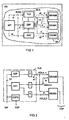
- a microprocessor or a microprocessor system MP is over one by address / data and status lines formed processor bus B with a control logic ALS connected, the one transmitting the data d Part of processor bus B by lines and that Address information ai transmitting part of the processor bus B is indicated by dashed lines.
- the processor bus B has, for example, a bus width of 32 bits and a processor clock speed from 33 MHz.
- a microprocessor system MP with such bus characteristics, for example the 486 DX microprocessor system from Intel.
- static partial memories SRAM ⁇ , 1 are connected to two static partial memories SRAM ⁇ , 1, in which, for example, the mediation program a telecommunications exchange is stored.
- processor bus B On processor bus B is also a control device ALD connected for dynamic memory DRAM. With help this commercial control device ALD will Writing and reading data to or from a dynamic DRAM memory controlled.
- the static partial memory SRAM ⁇ , 1 and the dynamic memory DRAM together form the main memory SP of the microprocessor system MP, being in the static Partial memories SRAM ⁇ , 1 those programs d or data d are stored for very short access times are provided.
- DRAM are in the dynamic memory of telecommunications switching systems especially data d with longer ones Access times saved.
- the two static partial memories SRAM ⁇ , 1 are by two static memory banks SRAM ⁇ , 1 formed, each of the static partial memory SRAM ⁇ , 1 separately via processor bus realized inputs E is controlled.
- the both with the static partial memories SRAM ⁇ , 1 and with is connected to the dynamic memory DRAM, the in read in or read the memories SRAM ⁇ , 1, DRAM Commands d or data d temporarily stored.
- the cache ZSP is advantageous due to a four-way buffer (4-Way Bus Exchange Buffer), the processor-controlled to both the static static memories SRAM ⁇ , 1 and the dynamic memory DRAM as well Microprocessor MP causes the temporary storage. This caching is especially suitable for the processor clock Transfer of commands d or data d to the memory DRAM, SRAM ⁇ , 1 required.
- Control logic ALS a clock and logic circuit TLS.
- the Clock and logic circuit TLS is the processor bus B to one Address buffer ASP, an address control AST and a buffer control ZSPS performed.
- the address buffer ASP are the microprocessor MP, address information represented by binary information ai4..n the address lines 4 to n, in the embodiment 4 to 31 cached and together with the in the address control AST formed address information ai2,3 the second and third address lines ADL 2,3 memory access to the two static Part memory SRAM ⁇ , 1 placed.
- Buffer control ZSPS provided with their help the data or commands in the static in accordance with the processor clock Part memory SRAM ⁇ , 1 registered or from the static Part memories SRAM ⁇ , 1 can be read.
- the function or the Operation of the clock and logic circuit TLS is as follows based on the flow chart shown in FIG 3 in more detail explained.
- the three memory sequence addresses sfa1..3 are formed on the basis of the address information ai of the first memory address sa1 of the first access Z according to an algorithm predefined both for the microprocessor MP and for the clock and logic circuit TLS.
- the first memory sequence address sfa1 is formed with the complementary logical information of the address bit with the value 2 2 .
- the second memory sequence address sfa2 is formed with the address bit of significance 2 2 of the first memory address sa1 and with the complementary logical information of the address bit of significance 2 3 .
- the complementary logical information of the address bits with the significance 2 2 and the significance 2 3 of the first memory address is used for the third memory sequence address sfa3.
- a sequence Q started from four memory accesses or accesses Z and starting from the first memory address sa1, the memory sequence addresses sfa1..3 formed according to FIG 3, wherein in the Control logic ALS after recognizing the first memory address sa1 the first memory address sa1 to the addressed partial memory SRAM ⁇ , 1 controlled or laid and almost simultaneously the first memory sequence address sfa1 is formed and on the other, not by the first memory address sfa1 addressed partial memory SRAM ⁇ , 1 controlled or set becomes.
- the one storage space within a partial memory SRAM ⁇ , 1 addressing partial address the first memory address sa1 remains unchanged.
- the first access to the memory SP or to a partial memory SRAM 0.1 occurs at memory access speed, i.e. the processor MP must, for example, by inserting waiting cycles - Known in the professional world as "wait-state" cycles Delay the access cycle, i.e. the access cycle time extend.
- the second memory address sfa2 formed and over the address lines ADL 2..n to the through the first memory address sa1 addressed partial memory SRAM ⁇ , 1 controlled or and read according to the status information or writing a date d initiated.
- control logic ASL by the first memory address sfa1 addressed partial memory SRAM ⁇ , 1 controlled - with Help with the first memory sequence address sfa1 - for example Date read d according to processor clock and according to processor cycle transferred to the buffer ZSP and on transferred the processor MP and the third memory sequence address sfa3 formed, to the respective partial memory SRAM ⁇ , 1 controlled or placed and according to the status information sti started reading or writing a date d.
- the inventive method according to FIG 3 is both program and also technically feasible, with the currently available microprocessors MP with high processing speeds a circuit implementation is preferable. It should be noted here that the formation the memory sequence addresses sfa1..3 and the alternate activation the partial memory SRAM 0.1 in accordance with the microprocessor clock is carried out. An arrangement for performing the invention The process is therefore based on processor speed and the number of processor clocks per access to be matched clock components. these are in particular processor clock controlled takeover registers or logical links. A detailed description a circuit design variant appears superfluous as it depends on the intended implementation through commercially available, user-programmable or customized circuits a variety of training courses is possible.
Landscapes
- Engineering & Computer Science (AREA)
- Theoretical Computer Science (AREA)
- Physics & Mathematics (AREA)
- General Engineering & Computer Science (AREA)
- General Physics & Mathematics (AREA)
- Memory System Of A Hierarchy Structure (AREA)
- Static Random-Access Memory (AREA)
Claims (8)
- Procédé pour commander une séquence (Q) prescrite d'accès (Z) d'un processeur (MP) par l'intermédiaire d'un bus (B) de processeur vers une mémoire (SP) d'écriture-lecture statique associée, formée par des sous-mémoires (SRAM Ø,1) pouvant être adressées individuellement, dans lequel les données (d) sont transférées du processeur (MP) ou au processeur (MP) chaque fois par l'intermédiaire d'une mémoire (ZSP) intermédiaire commandée par cycles d'accès et dans lequel un cycle (Z) d'accès à la mémoire (SP) commandé par l'intermédiaire du bus (B) de processeur comprend m cadences de processeur ainsi qu'un cycle d'écriture ou de lecture se déroulant dans la mémoire (SP) de n cadences de processeur, n étant supérieur à m,dans lequel une séquence (Q) d'accès (Z) est initiée par au moins une première adresse (sa1) de mémoire formée par le processeur et par des informations (sti) d'état qui commandent une lecture ou une écriture de donnée (d) dans ou sur la mémoire (SP) d'écriture-lecture statique,dans lequel, dans une logique (ALS) de commande insérée entre le processeur (MP) et les sous-mémoires (SRAM Ø,1),après réception de la première adresse (sa1) de mémoire par le processeur (MP), celle-ci est retransmise à la sous-mémoire (SRAM Ø,1) adressée et il est généré automatiquement et indépendamment du processeur (MP), pour les sous-mémoires (SRAM Ø,1) supplémentaires, chaque fois une adresse (sra1) suivante de mémoire en fonction de la séquence (Q) prescrite, les adresses (sfa1) suivantes de mémoire associée et la première adresse (sa1) de mémoire étant amenées séparément et simultanément à chaque sous-mémoire (SRAM Ø,1), ce qui fait qu'il est initié, en fonction des informations (sti) d'état, un cycle de lecture ou d'écriture dans toutes les sous-mémoires (SRAM Ø,1), età partir de la sous-mémoire (SRAM Ø,1) adressée par la première adresse (sa1) de mémoire, les sous-mémoires (SRAM Ø,1) sont commandées cycliquement en succession ainsi que conformément aux cycles d'accès, en fonction de la séquence (Q), pour une commande,en fonction des informations (sti) d'état, une donnée (d) lue, présente sur la sous-mémoire (SRAM Ø,1) commandée étant mise en mémoire dans la mémoire (ZSP) intermédiaire conformément à la cadence de processeur et enlevée de celle-ci par le processeur (MP) conformément aux cycles d'accès ou une donnée (d) transmise par le processeur (MP) étant mise en mémoire dans la mémoire (ZSP) intermédiaire et retransmise à la sous-mémoire (SRAM Ø,1) adressée,
la séquence (Q) d'accès (Z) étant terminée si une adresse suivante de mémoire formée par le processeur ne coïncide pas avec l'adresse (sfa1, sfa2, sfa3) de mémoire correspondante dans la succession, formée dans la logique (ALS) de commande, et,dans la mesure où cela est prévu en fonction de la séquence (Q) d'accès (Z), l'adresse (sa1, sfa1, sfa2) de mémoire du moment est changée, amenée à la sous-mémoire (SRAM Ø,1) commandée et, en fonction des informations (sti) d'état, un accès (Z) à la sous-mémoire (SRAM Ø,1) associée est initié. - Procédé suivant la revendication 1, caractérisé en ce que le nombre des sous-mémoires (SRAM Ø,1) est déterminé en fonction de la valeur absolue de la différence (n - m) entre le nombre n des cadences de processeur d'un cycle de lecture ou d'écriture se déroulant dans la mémoire (SP) et le nombre m des cadences de processeur d'un cycle (Z) d'accès à la mémoire (SP) commandé par l'intermédiaire du bus (B) de processeur.
- Procédé suivant l'une des revendications précédentes,
caractérisé en ce que, après la première adresse (sa1) de mémoire comprenant plusieurs bits d'adresses ayant le poids 2x, il est associé des adresses (sfa1, sfa2, sfa3) suivantes de mémoire prévues dans la logique (ALS) de commande pour l'adressage cyclique successif des sous-mémoires (SRAM Ø,1), en fonction de la séquence (Q) prescrite d'accès (Z), aux bits d'adresses d'informations (Ø,1) logiques représentant des informations (ai) d'adresses de telle manière que les sous-mémoires (SRAM Ø,1) sont adressées cycliquement en succession. - Procédé suivant la revendication 3, caractérisé en ce que, pour deux sous-mémoires (SRAM Ø,1) et une séquence (Q) de quatre cycles (Z) d'accès, pour une largeur de bus de processeur de 32 bits, il est formé pour un adressage cyclique successif des sous-mémoires (SRAM Ø,1), dans la logique (ALS) de commande, indépendamment du processeur (MP), à partir des informations (Ø,1) logiques, représentant les informations (ai) d'adresses, des bits d'adresses de la première adresse (sa1) de mémoire ayant le poids 22 et 23, trois adresses (sfa1, sfa2, sfa3) suivantes de mémoire,étant formées.la première adresse (sfa1) suivante de mémoire ayant l'information (Ø,1) logique complémentaire du bit d'adresse ayant le poids 22,la deuxième adresse (sfa2) suivante de mémoire ayant l'information (Ø,1) logique complémentaire du bit d'adresse ayant le poids 23, etla troisième adresse (sfa3) suivante de mémoire ayant l'information (Ø,1) logique complémentaire du bit d'adresse ayant le poids 22 et 23
- Procédé suivant l'une des revendications précédentes,
caractérisé en ce qu'un cycle (Z) d'accès conforme au processeur est exécuté en l'espace de deux ou trois cadences de processeur, le nombre des cadences de processeur étant, lors du premier cycle (Z) d'accès d'une séquence (Q), adapté à la durée d'accès à la mémoire (SP) et des cycles (Z) d'accès conformes au processeur étant prévus pour les cycles (Z) d'accès supplémentaires d'une séquence (Q). - Dispositif de commande d'une séquence (Q) prescrite d'accès (Z) d'un processeur (MP) à une mémoire (SP) associée, formée par des sous-mémoires (SRAM Ø,1) pouvant être adressées individuellement, par l'intermédiaire d'un bus (B) de processeur, un cycle (Z) d'accès à la mémoire (SP) commandé par l'intermédiaire du bus (B) de processeur comportant m cadences de processeur et un cycle de lecture ou d'écriture se déroulant dans la mémoire (SP) comportant n cadences de processeur, n étant supérieur à m,caractérisédans lequel une logique (ALS) de commande est insérée entre le processeur (MP) et les sous-mémoires (SRAM Ø,1),comportant une mémoire intermédiaire (ZSP) commandée par cycles d'accès pour transférer les données (d) entre le processeur (MP) et la mémoire (SP) d'écriture-lecture statique,comportant des moyens de commande pour introduire une séquence (Q) d'accès (Z) par au moins une première adresse (sa1) de mémoire, formée par le processeur (MP), et par des informations (sti) d'état qui commandent une lecture ou une écriture de données dans ou sur la mémoire (SP) d'écriture-lecture statique, etcomportant des moyens d'accès à la mémoire pour l'accès successif de manière cyclique ainsi que conforme aux cycles d'accès aux sous-mémoires (SRAM Ø,1) à partir de la sous-mémoire (SRAM Ø,1) adressée par la première adresse (sa1) de mémoire, en fonction de la séquence (Q), lors de l'accèsune donnée (d) lue, présente sur la sous-mémoire (SRAM Ø,1) commandée, étant, en fonction des informations (sti) d'état, mise en mémoire dans la mémoire (ZST) intermédiaire et enlevée de celle-ci par le processeur (MP) conformément aux cycles d'accès ou une donnée (d) transmise par le processeur (MP) étant mémorisée dans la mémoire (ZSP) intermédiaire associée, commandée à la cadence de processeur, ainsi que retransmise à la sous-mémoire (SRAM Ø,1) adressée,en ce que la mémoire (SP) est réalisée en mémoire d'écriture-lecture statique, eten ce que la logique (ALS) de commandecomporte un dispositif pour générer des adresses en vue de générer de manière autonome, en partant de la première adresse (sa1) de mémoire, une adresse (sfa1) suivante d'adresse associée pour les sous-mémoires (SRAM Ø,1) supplémentaires, en fonction de la séquence (Q) prescrite, ainsi que pour appliquer séparément et simultanément la première adresse (sa1) de mémoire ainsi que les adresses (sfa1) suivantes de mémoire chaque fois générées à chaque sous-mémoire (SRAM Ø,1), ce qui fait que, en fonction des informations (sti) d'état, un cycle de lecture ou d'écriture est initié dans toutes les sous-mémoires (SRAM Ø,1), etcomporte un dispositif de comparaison pour comparer une adresse suivante de mémoire formée par le processeur (MP) à une adresse (sfa1, sfa2, sfa3) suivante de mémoire formée par le dispositif (AST) pour générer des adresses, correspondantes dans la succession, et pour mettre fin à la séquence (Q) d'accès (Z) en cas de non coïncidence.
- Procédé suivant la revendication 6, caractérisé en ce que la logique (ALS) de commande est formée par un circuit (TLS) logique et d'horloge et par la mémoire (ZSP) intermédiaire, et en ce que le circuit (TLS) logique et d'horlogecomporte une mémoire (ASP) intermédiaire d'adresses et est relié aux lignes (ADL4 ..n) d'adresses du bus (B) de processeur dont les informations (ai) d'adresses sont à retransmettre de manière inchangée aux sous-mémoires (SRAM Ø,1), les informations (ai) d'adresses étant mises en mémoire dans la mémoire (ASP) intermédiaire d'adresses cadencées par le processeur et étant envoyées conformément aux cycles d'accès, par l'intermédiaire de lignes (ADL4 ..n) lignes d'adresses supplémentaires, aux sous-mémoires (SRAM Ø,1), etest muni d'une commande (AST) d'adresses et est relié aux lignes (ADL2, 3) d'adresses du bus de processeur dont les informations (ai) d'adresses sont retransmises lors du premier cycle (Z) d'accès à la sous-mémoire (SRAM Ø,1) adressée et dont les informations (ai) d'adresses suivantes sont formées lors des cycles (Z) d'accès suivants d'une séquence (Q) dans la commande (AST) d'adresses, sont vérifiées et sont envoyées aux sous-mémoires (SRAM Ø,1) concernées, etest formé par une commande (ZSPS) de mémoire intermédiaire commandant la mémoire (ZSP) intermédiaire.
- Dispositif suivant la revendication 6 ou 7, caractérisé en ce que le microprocesseur (MP) et la mémoire (ZSP) intermédiaire sont reliés à un dispositif (ALD) de commande pour des mémoires (DRAM) dynamiques et en ce que le dispositif (ALD) de commande et la mémoire (ZSP) intermédiaire sont reliés en vue d'une lecture et d'une écriture de données (d) à une mémoire (DRAM) dynamique, la mémoire (DRAM) dynamique comportant de plus grandes durées d'accès par rapport aux sous-mémoires (SRAM Ø,1) statiques.
Applications Claiming Priority (2)
| Application Number | Priority Date | Filing Date | Title |
|---|---|---|---|
| DE4427042 | 1994-07-29 | ||
| DE4427042A DE4427042C2 (de) | 1994-07-29 | 1994-07-29 | Verfahren zur Steuerung einer Sequenz von Zugriffen eines Prozessors zu einem zugeordneten Speicher |
Publications (2)
| Publication Number | Publication Date |
|---|---|
| EP0694843A1 EP0694843A1 (fr) | 1996-01-31 |
| EP0694843B1 true EP0694843B1 (fr) | 2001-10-17 |
Family
ID=6524538
Family Applications (1)
| Application Number | Title | Priority Date | Filing Date |
|---|---|---|---|
| EP95111343A Expired - Lifetime EP0694843B1 (fr) | 1994-07-29 | 1995-07-19 | Procédé et dispositif de commande d'une séquence d'accès de processeur à une mémoire associée |
Country Status (3)
| Country | Link |
|---|---|
| US (1) | US5754815A (fr) |
| EP (1) | EP0694843B1 (fr) |
| DE (2) | DE4427042C2 (fr) |
Families Citing this family (9)
| Publication number | Priority date | Publication date | Assignee | Title |
|---|---|---|---|---|
| US5940443A (en) * | 1994-11-04 | 1999-08-17 | Harris Corporation | Parallel telephone bus segmentation system |
| US5838631A (en) | 1996-04-19 | 1998-11-17 | Integrated Device Technology, Inc. | Fully synchronous pipelined ram |
| FR2748595B1 (fr) * | 1996-05-10 | 1998-07-10 | Sgs Thomson Microelectronics | Memoire a acces parallele |
| US5933385A (en) * | 1997-07-31 | 1999-08-03 | Integrated Silicon Solution Inc. | System and method for a flexible memory controller |
| US6115320A (en) | 1998-02-23 | 2000-09-05 | Integrated Device Technology, Inc. | Separate byte control on fully synchronous pipelined SRAM |
| US7069406B2 (en) * | 1999-07-02 | 2006-06-27 | Integrated Device Technology, Inc. | Double data rate synchronous SRAM with 100% bus utilization |
| JP2001034530A (ja) * | 1999-07-16 | 2001-02-09 | Mitsubishi Electric Corp | マイクロコンピュータおよびメモリアクセス制御方法 |
| DE60308150T2 (de) * | 2002-02-06 | 2007-07-19 | Koninklijke Philips Electronics N.V. | Adressenraum, bussystem, speicherungssteuerung und einrichtungssystem |
| CN114385083B (zh) * | 2022-01-07 | 2023-05-23 | 烽火通信科技股份有限公司 | 一种数据帧统计采集装置及方法 |
Family Cites Families (5)
| Publication number | Priority date | Publication date | Assignee | Title |
|---|---|---|---|---|
| US5247644A (en) * | 1991-02-06 | 1993-09-21 | Advanced Micro Devices, Inc. | Processing system with improved sequential memory accessing |
| EP0530991A1 (fr) * | 1991-09-05 | 1993-03-10 | NCR International, Inc. | Système et procédé d'entrelacement de mémoire dans un système d'ordinateur |
| US5345573A (en) * | 1991-10-04 | 1994-09-06 | Bull Hn Information Systems Inc. | High speed burst read address generation with high speed transfer |
| JP3299564B2 (ja) * | 1992-05-11 | 2002-07-08 | 松下電器産業株式会社 | メモリ装置 |
| JPH06149662A (ja) * | 1992-11-02 | 1994-05-31 | Toshiba Corp | Romバースト転送の連続読みだし拡大方式およびその方式を用いたrom内蔵型マイクロコンピュータシステム |
-
1994
- 1994-07-29 DE DE4427042A patent/DE4427042C2/de not_active Expired - Fee Related
-
1995
- 1995-07-19 DE DE59509707T patent/DE59509707D1/de not_active Expired - Fee Related
- 1995-07-19 EP EP95111343A patent/EP0694843B1/fr not_active Expired - Lifetime
- 1995-07-28 US US08/508,968 patent/US5754815A/en not_active Expired - Fee Related
Also Published As
| Publication number | Publication date |
|---|---|
| EP0694843A1 (fr) | 1996-01-31 |
| US5754815A (en) | 1998-05-19 |
| DE59509707D1 (de) | 2001-11-22 |
| DE4427042C2 (de) | 1997-05-22 |
| DE4427042A1 (de) | 1996-02-01 |
Similar Documents
| Publication | Publication Date | Title |
|---|---|---|
| DE3724317C2 (fr) | ||
| DE2617408C3 (de) | Speichermodul fur ein Datenverarbeitungsgerät mit Speicherhierarchie | |
| DE69625486T2 (de) | Speichersteuerung zur nicht sequentiellen ausführung von schreibbefehlen | |
| DE1956604C3 (de) | Datenverarbeitungsanlage | |
| DE2630323A1 (de) | Datenspeichereinrichtung | |
| EP0013737A1 (fr) | Hiérarchie de mémoire à plusieurs étages pour un système de traitement des données | |
| DE2922597A1 (de) | Cache-speicher und verfahren zum betrieb einer datenverarbeitungsanlage | |
| DE69330819T2 (de) | Synchrone LSI-Speicheranordnung | |
| DE2432608C3 (de) | Speicheranordnung fur eine Datenverarbeitungseinrichtung | |
| DE3934145A1 (de) | Platteneinheit-steuerungsvorrichtung und informationsverarbeitungssystem, das dieselbe enthaelt | |
| EP0694843B1 (fr) | Procédé et dispositif de commande d'une séquence d'accès de processeur à une mémoire associée | |
| DE69330923T2 (de) | Verschachteltes Speichersystem | |
| DE69025782T2 (de) | Registerbankschaltung | |
| EP0409330B1 (fr) | Circuit de commande d'accès d'une mémoire | |
| DE3852204T2 (de) | Datenübertragungsvorrichtung und Datenübertragungsverfahren zur Anwendung in einer Datenverarbeitungsanordnung. | |
| EP0609703A2 (fr) | Dispositif de mémoire intégrée monolithique et méthode de son fonctionnement | |
| DE2610428A1 (de) | Anordnung zur steuerung der zwischenspeicherung von zwischen zwei funktionseinheiten zu uebertragenden daten in einem pufferspeicher | |
| DE102004005275A1 (de) | Adressenpuffer für einen Halbleiterbaustein | |
| EP1435578B1 (fr) | Contrôleur DMA pour la mise-à-jour des descripteurs dans la mémoire après chaque accès | |
| DE19537905C2 (de) | Speicherzugriffsvorrichtung und -verfahren | |
| DE19748675A1 (de) | Vorausleseverfahren für ein Speicherbauelement und einen Speicheraufbau unter Verwendung des Vorausleseverfahrens | |
| DE2854286A1 (de) | Schaltungsanordnung mit einem befehlspuffer fuer eine cachespeichereinheit eines datenverarbeitungssystems | |
| DE19846914C2 (de) | Datenbus und Verfahren zum Kommunizieren zweier Baugruppen mittels eines solchen Datenbusses | |
| DE69334046T2 (de) | Cache-Speichervorrichtung | |
| DE10025952B4 (de) | Datenverarbeitungseinheit mit einer Superscaler-Struktur sowie Verfahren zum Zuführen einer Mehrzahl von Befehlen |
Legal Events
| Date | Code | Title | Description |
|---|---|---|---|
| PUAI | Public reference made under article 153(3) epc to a published international application that has entered the european phase |
Free format text: ORIGINAL CODE: 0009012 |
|
| AK | Designated contracting states |
Kind code of ref document: A1 Designated state(s): DE FR GB IT |
|
| 17P | Request for examination filed |
Effective date: 19960719 |
|
| 17Q | First examination report despatched |
Effective date: 19990616 |
|
| GRAG | Despatch of communication of intention to grant |
Free format text: ORIGINAL CODE: EPIDOS AGRA |
|
| RTI1 | Title (correction) |
Free format text: METHOD AND DEVICE FOR CONTROLLING A SEQUENCE OF PROCESSOR ACCESSES TO AN ASSOCIATED MEMORY |
|
| GRAG | Despatch of communication of intention to grant |
Free format text: ORIGINAL CODE: EPIDOS AGRA |
|
| GRAH | Despatch of communication of intention to grant a patent |
Free format text: ORIGINAL CODE: EPIDOS IGRA |
|
| GRAH | Despatch of communication of intention to grant a patent |
Free format text: ORIGINAL CODE: EPIDOS IGRA |
|
| GRAA | (expected) grant |
Free format text: ORIGINAL CODE: 0009210 |
|
| AK | Designated contracting states |
Kind code of ref document: B1 Designated state(s): DE FR GB IT |
|
| REF | Corresponds to: |
Ref document number: 59509707 Country of ref document: DE Date of ref document: 20011122 |
|
| REG | Reference to a national code |
Ref country code: GB Ref legal event code: IF02 |
|
| GBT | Gb: translation of ep patent filed (gb section 77(6)(a)/1977) |
Effective date: 20020105 |
|
| ET | Fr: translation filed | ||
| PLBE | No opposition filed within time limit |
Free format text: ORIGINAL CODE: 0009261 |
|
| STAA | Information on the status of an ep patent application or granted ep patent |
Free format text: STATUS: NO OPPOSITION FILED WITHIN TIME LIMIT |
|
| 26N | No opposition filed | ||
| PGFP | Annual fee paid to national office [announced via postgrant information from national office to epo] |
Ref country code: DE Payment date: 20030916 Year of fee payment: 9 |
|
| PGFP | Annual fee paid to national office [announced via postgrant information from national office to epo] |
Ref country code: GB Payment date: 20040708 Year of fee payment: 10 |
|
| PGFP | Annual fee paid to national office [announced via postgrant information from national office to epo] |
Ref country code: FR Payment date: 20040716 Year of fee payment: 10 |
|
| PG25 | Lapsed in a contracting state [announced via postgrant information from national office to epo] |
Ref country code: DE Free format text: LAPSE BECAUSE OF NON-PAYMENT OF DUE FEES Effective date: 20050201 |
|
| PG25 | Lapsed in a contracting state [announced via postgrant information from national office to epo] |
Ref country code: IT Free format text: LAPSE BECAUSE OF NON-PAYMENT OF DUE FEES;WARNING: LAPSES OF ITALIAN PATENTS WITH EFFECTIVE DATE BEFORE 2007 MAY HAVE OCCURRED AT ANY TIME BEFORE 2007. THE CORRECT EFFECTIVE DATE MAY BE DIFFERENT FROM THE ONE RECORDED. Effective date: 20050719 Ref country code: GB Free format text: LAPSE BECAUSE OF NON-PAYMENT OF DUE FEES Effective date: 20050719 |
|
| GBPC | Gb: european patent ceased through non-payment of renewal fee |
Effective date: 20050719 |
|
| PG25 | Lapsed in a contracting state [announced via postgrant information from national office to epo] |
Ref country code: FR Free format text: LAPSE BECAUSE OF NON-PAYMENT OF DUE FEES Effective date: 20060331 |
|
| REG | Reference to a national code |
Ref country code: FR Ref legal event code: ST Effective date: 20060331 |