EP0333018A2 - Lentille d'objectif pour la focalisation de particules chargées - Google Patents
Lentille d'objectif pour la focalisation de particules chargées Download PDFInfo
- Publication number
- EP0333018A2 EP0333018A2 EP89104133A EP89104133A EP0333018A2 EP 0333018 A2 EP0333018 A2 EP 0333018A2 EP 89104133 A EP89104133 A EP 89104133A EP 89104133 A EP89104133 A EP 89104133A EP 0333018 A2 EP0333018 A2 EP 0333018A2
- Authority
- EP
- European Patent Office
- Prior art keywords
- electrode
- lens
- objective lens
- magnetic
- sample
- Prior art date
- Legal status (The legal status is an assumption and is not a legal conclusion. Google has not performed a legal analysis and makes no representation as to the accuracy of the status listed.)
- Granted
Links
- 239000002245 particle Substances 0.000 title claims description 5
- 238000007654 immersion Methods 0.000 claims abstract description 17
- 239000011163 secondary particle Substances 0.000 claims 2
- 230000005684 electric field Effects 0.000 abstract description 2
- 239000000523 sample Substances 0.000 description 14
- 230000000694 effects Effects 0.000 description 6
- 230000001133 acceleration Effects 0.000 description 4
- 230000004075 alteration Effects 0.000 description 3
- 230000008859 change Effects 0.000 description 3
- 238000003384 imaging method Methods 0.000 description 3
- 230000007935 neutral effect Effects 0.000 description 3
- 230000009467 reduction Effects 0.000 description 3
- 230000001960 triggered effect Effects 0.000 description 3
- 230000008901 benefit Effects 0.000 description 2
- 238000011161 development Methods 0.000 description 2
- 230000018109 developmental process Effects 0.000 description 2
- 238000010894 electron beam technology Methods 0.000 description 2
- 230000006872 improvement Effects 0.000 description 2
- 230000033228 biological regulation Effects 0.000 description 1
- 230000007423 decrease Effects 0.000 description 1
- 230000001419 dependent effect Effects 0.000 description 1
- 230000002349 favourable effect Effects 0.000 description 1
- 239000012212 insulator Substances 0.000 description 1
- 230000003993 interaction Effects 0.000 description 1
- 238000004519 manufacturing process Methods 0.000 description 1
- 239000000463 material Substances 0.000 description 1
- 238000005259 measurement Methods 0.000 description 1
- 238000004377 microelectronic Methods 0.000 description 1
- 230000005693 optoelectronics Effects 0.000 description 1
- 239000004065 semiconductor Substances 0.000 description 1
- 238000012876 topography Methods 0.000 description 1
Images

Classifications
-
- H—ELECTRICITY
- H01—ELECTRIC ELEMENTS
- H01J—ELECTRIC DISCHARGE TUBES OR DISCHARGE LAMPS
- H01J37/00—Discharge tubes with provision for introducing objects or material to be exposed to the discharge, e.g. for the purpose of examination or processing thereof
- H01J37/02—Details
- H01J37/04—Arrangements of electrodes and associated parts for generating or controlling the discharge, e.g. electron-optical arrangement or ion-optical arrangement
- H01J37/10—Lenses
- H01J37/145—Combinations of electrostatic and magnetic lenses
Definitions
- the invention relates to an objective lens for focusing charged particles.
- the invention has for its object to provide an objective lens of the type mentioned, with which a charge-neutral examination of poorly conductive samples is guaranteed. This object is achieved by an objective lens according to claim 1.
- the advantage that can be achieved with the invention is, in particular, that non-conductive or poorly conductive samples can be imaged and measured with high resolution and with no charge.
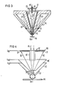
- 1 to 4 show exemplary embodiments of objective lenses according to the invention for scanning electron microscopes.
- the objective lens shown schematically in FIG. 1 forms the component of a scanning electron microscope with which an electron source or its intermediate image reduced by condenser lenses is imaged on the sample PR, in particular an opto or microelectronic component.
- the objective lens consists of an asymmetrical magnetic lens ML, an electrostatic immersion lens OE / UE superimposed on the magnetic lens ML, a control electrode ST which is at an adjustable potential and a detector DT for detecting the secondary and backscattered electrons SE triggered by the primary electrons PE at the respective measuring point.
- the immersion lens comprises a conical electrode OE, which is insulated in the area of the upper pole shoe OP of the magnetic lens ML, and a tubular electrode UE which projects into the bore of the lower pole shoe UP and whose potentials U OE or U UE are selected such that they are within the objective lens decelerating the primary electrons PE or building up an electric field accelerating the secondary electrons SE.
- the color and aperture error constants of the magnetic lens ML exceed those of the electrostatic-magnetic objective lens by almost an order of magnitude if the primary electrons PE are braked by a factor of 10 in the field of the immersion lens.
- the detector DT for detecting the secondary and backscattered electrons SE triggered at the respective measuring point and accelerated in the field of the immersion lens is located in the exemplary embodiment shown directly above the magnetic lens ML arranges. It consists of a ring-shaped electron-sensitive part ES and a hollow cylinder RE which is insulated in its central bore.
- U ES 10 kV
- the hollow cylinder RE which has a positive potential U RE of, for example, U OE - 1 kV ⁇ U RE ⁇ U OE, should reach into the upper one Reach in the pole shoe hole of the ML magnetic lens.
- detectors DT semiconductor detectors, channel plates or scintillator-light guide combinations come into consideration as detectors DT, which, in contrast to FIG. 1, can also be arranged within the objective lens.
- ring-shaped detectors DT have the advantage that almost all of the secondary electrons SE extracted from the sample PR in the field of the immersion lens can be detected.
- Quadrant detectors can of course also be used.
- i PR denotes the sample current, i PE the primary electron current, i RE the backscattered electron current and i SE the secondary electron current.
- Such a scanning electron microscope equipped with the objective lens according to the invention does not require such a change in the beam energy E PE with the associated disadvantages (change in the acceleration voltage, refocusing of the primary electron beam, readjustment of the stigmator field), since the intensity of the secondary electron current i SE can be determined using the electrode arranged below the magnetic lens ML ST (regulation of the strength of the suction field acting on the secondary electrons SE) can weaken or increase to the required extent.
- the resolution at low acceleration voltages below about 5 kV (the neutral point energies are, with a few exceptions, in the energy range between about 0.5 and 4 keV) is essentially limited by the Boersch effect and the color error of the objective lens.
- the Coulomb repulsion of the electrons their spatial distance and thus the beam diameter on the sample increases (lateral Boersch effect).
- the electron-electron interaction in areas of high current densities, in particular in the beam generator and in the beam crossing points leads to a broadening of the energy distribution of the primary electrons (energetic Boersch effect), which has an unfavorable effect on the probe diameter via the chromatic aberration of the objective lens .
- the objective lens according to the invention which replaces the conventional objective lens of the scanning electron microscope with its comparatively large aberration, is preferably used as a device for braking and focusing the primary electrons.
- the improvement in the imaging properties results from the reduction in the color and aperture error constants associated with the deceleration of the primary electrons PE, but also from the shift of the main plane of the lens ML in the direction of the sample PR (reduction of the focal length f), which in turn has a favorable effect on that of the focal length f proportional color error constant C F affects.
- the electrode ST for setting the strength of the suction field acting on the secondary electrons SE is likewise arranged directly below the magnetic lens ML and is preferably frustoconical.
- the electrode ST can also be integrated into the lower pole shoe UP of the magnetic lens ML by applying the desired potential U ST to the lower part UP1, which is separated from the upper pole shoe part by an insulator IS.
- FIG. 4 shows an electrostatic objective lens (immersion lens with central electrode) whose source-side electrode OE has an annular part RB which acts as an aperture and a hollow cylinder HZ which extends in the direction of the sample PR.
- the center electrode ME which is at a variable positive potential U ME
- the sample-side electrode UE and the electrode ST for controlling the intensity of the secondary electron current emanating from the sample PR are each frustoconical in the exemplary embodiment and arranged concentrically to the axis OA of the hollow cylinder HZ.
- the side faces of the conical electrodes ME, UE or ST should preferably form an angle ⁇ 'between about 30 and 70 ° with the axis OA.
- the detector DT for detecting the secondary electrons SE triggered on the sample PR is arranged within the objective lens between the source-side and the middle electrode OE or ME. It consists of a ring-shaped electron sensitive Part that is preferably segmented. Since the hollow cylinder HZ is at a somewhat lower potential U HZ than the center electrode ME (U HZ ⁇ U ME ), the secondary electrons SE emitted in the direction of the beam axis OA are also deflected and detected towards the detector DT.
- This lens can also preferably be used as a lens in a high-resolution scanning electron microscope in order to brake the primary electrons PE accelerated to high kinetic energies to the desired final energy.
- the electrode OE is then subjected to the potential of the anode of the beam generator, for example, while the electrode UE is at the potential of the sample PR, that is to say usually at ground.
- the invention is of course not limited to the exemplary embodiments described. So it is easily possible to replace the conical electrode OE with a tubular electrode. However, it is important to ensure that the tube diameter is larger than the maximum cross section of the diverging secondary electron beam generated within the objective lens.
- the lower pole piece can also serve as the second electrode of the immersion lens.
- a significant improvement in the resolution of a scanning electron microscope can be expected in particular if the energy of the primary electrons is reduced by at least a factor of two using the objective lens according to the invention.
Landscapes
- Chemical & Material Sciences (AREA)
- Analytical Chemistry (AREA)
- Analysing Materials By The Use Of Radiation (AREA)
Applications Claiming Priority (2)
| Application Number | Priority Date | Filing Date | Title |
|---|---|---|---|
| DE3809014 | 1988-03-17 | ||
| DE3809014 | 1988-03-17 |
Publications (3)
| Publication Number | Publication Date |
|---|---|
| EP0333018A2 true EP0333018A2 (fr) | 1989-09-20 |
| EP0333018A3 EP0333018A3 (en) | 1990-07-04 |
| EP0333018B1 EP0333018B1 (fr) | 1994-06-01 |
Family
ID=6350018
Family Applications (1)
| Application Number | Title | Priority Date | Filing Date |
|---|---|---|---|
| EP89104133A Expired - Lifetime EP0333018B1 (fr) | 1988-03-17 | 1989-03-08 | Lentille d'objectif pour la focalisation de particules chargées |
Country Status (4)
| Country | Link |
|---|---|
| US (1) | US4926054A (fr) |
| EP (1) | EP0333018B1 (fr) |
| JP (1) | JP2887602B2 (fr) |
| DE (1) | DE58907728D1 (fr) |
Cited By (10)
| Publication number | Priority date | Publication date | Assignee | Title |
|---|---|---|---|---|
| DE19605855A1 (de) * | 1996-02-16 | 1997-08-21 | Act Advanced Circuit Testing | Detektorobjektiv für Korpuskularstrahlgeräte |
| EP0821393A1 (fr) * | 1996-07-25 | 1998-01-28 | ACT Advanced Circuit Testing Gesellschaft für Testsystementwicklung mbH | Lentille objectif de détecteur |
| WO1998014979A1 (fr) * | 1996-10-04 | 1998-04-09 | Etec Systems, Inc. | Montage d'un detecteur de particules transistorise dans un champ de deviation magnetique |
| EP1022766A1 (fr) * | 1998-11-30 | 2000-07-26 | Advantest Corporation | Appareil à faisceau de particules |
| EP1052679A1 (fr) * | 1999-05-06 | 2000-11-15 | Advantest Corporation | Appareil à faisceau corpusculaire |
| DE10233002A1 (de) * | 2002-07-19 | 2004-02-12 | Leo Elektronenmikroskopie Gmbh | Objektivlinse für ein Elektronenmikroskopiesystem und Elektronenmikroskopiesystem |
| US6949744B2 (en) | 2003-04-17 | 2005-09-27 | Carl Zeiss Nts Gmbh | Electron microscopy system, electron microscopy method and focusing system for charged particles |
| EP2270835A3 (fr) * | 2005-11-28 | 2011-02-23 | Carl Zeiss SMT AG | Composant optique corpusculaire |
| EP1028452B1 (fr) * | 1992-10-20 | 2012-03-28 | Hitachi, Ltd. | Microscope électronique à balayage |
| CZ307259B6 (cs) * | 2016-09-26 | 2018-05-02 | Tescan Brno, S.R.O. | Objektivová čočka pro zařízení využívající nejméně jednoho svazku nabitých částic |
Families Citing this family (45)
| Publication number | Priority date | Publication date | Assignee | Title |
|---|---|---|---|---|
| JPH071681B2 (ja) * | 1990-04-19 | 1995-01-11 | 株式会社日立製作所 | 荷電粒子線装置 |
| DE69233781D1 (de) * | 1991-11-27 | 2010-04-01 | Hitachi Ltd | Elektronenstrahlgerät |
| JP2919170B2 (ja) * | 1992-03-19 | 1999-07-12 | 株式会社日立製作所 | 走査電子顕微鏡 |
| KR970005769B1 (ko) * | 1992-08-27 | 1997-04-19 | 가부시끼가이샤 도시바 | 자계 계침형 전자총 |
| EP0767482B1 (fr) * | 1994-04-12 | 1999-09-22 | Koninklijke Philips Electronics N.V. | Appareil optique à particules comprenant un sélecteur d'électrons secondaires |
| US5644132A (en) * | 1994-06-20 | 1997-07-01 | Opan Technologies Ltd. | System for high resolution imaging and measurement of topographic and material features on a specimen |
| DE69638126D1 (de) * | 1995-10-19 | 2010-04-01 | Hitachi Ltd | Rasterelektronenmikroskop |
| DE69633338T2 (de) * | 1996-11-19 | 2005-02-24 | Advantest Corp. | Elektrostatische Vorrichtung zur Einwirkung auf einen Korpuskularstrahl |
| US6069363A (en) * | 1998-02-26 | 2000-05-30 | International Business Machines Corporation | Magnetic-electrostatic symmetric doublet projection lens |
| DE19828476A1 (de) | 1998-06-26 | 1999-12-30 | Leo Elektronenmikroskopie Gmbh | Teilchenstrahlgerät |
| GB2348048A (en) | 1999-03-19 | 2000-09-20 | Shimadzu Research Lab | Magnetic immersion lenses |
| EP1238405B1 (fr) * | 1999-12-14 | 2014-06-18 | Applied Materials, Inc. | Procede et systeme d'examen d'un echantillon avec un faisceau de particules chargees |
| US6380546B1 (en) * | 2000-01-01 | 2002-04-30 | Applied Materials, Inc. | Focusing assembly and method for a charged particle beam column |
| DE10012314A1 (de) | 2000-03-14 | 2001-09-20 | Leo Elektronenmikroskopie Gmbh | Detektorsystem für ein Korpuskularstrahlgerät und Korpuskularstrahlgerät mit einem solchen Detektorsystem |
| DE60038007T2 (de) * | 2000-05-31 | 2008-05-29 | Advantest Corporation | Teilchenstrahlgerät |
| EP2587515A1 (fr) * | 2000-06-27 | 2013-05-01 | Ebara Corporation | Système d'inspection par faisceau de particules chargées et procédé de fabrication de dispositifs utilisant ledit système |
| DE60118070T2 (de) * | 2001-09-04 | 2006-08-17 | Advantest Corp. | Partikelstrahlgerät |
| US20050103272A1 (en) * | 2002-02-25 | 2005-05-19 | Leo Elektronenmikroskopie Gmbh | Material processing system and method |
| US7528614B2 (en) | 2004-12-22 | 2009-05-05 | Applied Materials, Inc. | Apparatus and method for voltage contrast analysis of a wafer using a tilted pre-charging beam |
| US6897442B2 (en) * | 2003-04-25 | 2005-05-24 | Applied Materials Israel, Ltd. | Objective lens arrangement for use in a charged particle beam column |
| KR101041661B1 (ko) * | 2003-07-30 | 2011-06-14 | 어플라이드 머티리얼즈 이스라엘 리미티드 | 다중 검출기들을 갖는 스캐닝 전자 현미경 및 다중 검출기기반 이미징을 위한 방법 |
| US7842933B2 (en) * | 2003-10-22 | 2010-11-30 | Applied Materials Israel, Ltd. | System and method for measuring overlay errors |
| US7233008B1 (en) * | 2005-03-14 | 2007-06-19 | Applied Materials, Israel, Ltd. | Multiple electrode lens arrangement and a method for inspecting an object |
| EP1703538B1 (fr) * | 2005-03-17 | 2008-11-12 | ICT Integrated Circuit Testing Gesellschaft für Halbleiterprüftechnik mbH | Dispositif à faisceau de particules chargées pour haute résolution spatiale et pour imagerie en perspectives multiples |
| EP1777728A1 (fr) * | 2005-10-20 | 2007-04-25 | Carl Zeiss SMS GmbH | Sytème lithographique |
| DE102006059162B4 (de) * | 2006-12-14 | 2009-07-09 | Carl Zeiss Nts Gmbh | Teilchenoptische Anordnung |
| US8698093B1 (en) | 2007-01-19 | 2014-04-15 | Kla-Tencor Corporation | Objective lens with deflector plates immersed in electrostatic lens field |
| US7872236B2 (en) * | 2007-01-30 | 2011-01-18 | Hermes Microvision, Inc. | Charged particle detection devices |
| DE102007010873B4 (de) * | 2007-03-06 | 2009-07-30 | Carl Zeiss Nts Gmbh | Objektivlinse |
| DE602007005631D1 (de) * | 2007-07-27 | 2010-05-12 | Integrated Circuit Testing | Elektrostatische Linsenanordnung |
| US7759653B2 (en) * | 2008-05-30 | 2010-07-20 | Hermes Microvision, Inc. | Electron beam apparatus |
| US7960697B2 (en) | 2008-10-23 | 2011-06-14 | Hermes-Microvision, Inc. | Electron beam apparatus |
| US7919760B2 (en) * | 2008-12-09 | 2011-04-05 | Hermes-Microvision, Inc. | Operation stage for wafer edge inspection and review |
| US8094924B2 (en) * | 2008-12-15 | 2012-01-10 | Hermes-Microvision, Inc. | E-beam defect review system |
| EP2365514B1 (fr) * | 2010-03-10 | 2015-08-26 | ICT Integrated Circuit Testing Gesellschaft für Halbleiterprüftechnik mbH | Colonne de particules chargées de faisceau double et son procédé de contrôle |
| US8735030B2 (en) | 2010-04-15 | 2014-05-27 | Carl Zeiss Smt Gmbh | Method and apparatus for modifying a substrate surface of a photolithographic mask |
| JP5530811B2 (ja) * | 2010-06-02 | 2014-06-25 | 株式会社日立ハイテクノロジーズ | 走査電子顕微鏡装置 |
| EP2518755B1 (fr) | 2011-04-26 | 2014-10-15 | FEI Company | Détecteur "in-column" pour colonne d'optique corpusculaire |
| US9046475B2 (en) | 2011-05-19 | 2015-06-02 | Applied Materials Israel, Ltd. | High electron energy based overlay error measurement methods and systems |
| US10008360B2 (en) | 2015-01-26 | 2018-06-26 | Hermes Microvision Inc. | Objective lens system for fast scanning large FOV |
| JP6814282B2 (ja) * | 2017-03-29 | 2021-01-13 | 株式会社日立ハイテク | 荷電粒子線装置 |
| US10777382B2 (en) | 2017-11-21 | 2020-09-15 | Focus-Ebeam Technology (Beijing) Co., Ltd. | Low voltage scanning electron microscope and method for specimen observation |
| US10438769B1 (en) * | 2018-05-02 | 2019-10-08 | Kla-Tencor Corporation | Array-based characterization tool |
| CN114220725B (zh) | 2020-12-02 | 2024-05-07 | 聚束科技(北京)有限公司 | 一种电子显微镜 |
| CN114256043B (zh) | 2020-12-02 | 2024-04-05 | 聚束科技(北京)有限公司 | 一种电子束系统 |
Family Cites Families (4)
| Publication number | Priority date | Publication date | Assignee | Title |
|---|---|---|---|---|
| DE3236271A1 (de) * | 1982-09-30 | 1984-04-05 | Siemens AG, 1000 Berlin und 8000 München | Spektrometerobjektiv fuer die korpuskularstrahl-messtechnik |
| US4596929A (en) * | 1983-11-21 | 1986-06-24 | Nanometrics Incorporated | Three-stage secondary emission electron detection in electron microscopes |
| EP0242602B1 (fr) * | 1986-04-24 | 1993-07-21 | ICT Integrated Circuit Testing Gesellschaft für Halbleiterprüftechnik mbH | Lentille électrostatique et magnétique pour appareils à faisceau corpusculaire |
| EP0274622B1 (fr) * | 1986-12-12 | 1990-11-07 | ICT Integrated Circuit Testing Gesellschaft für Halbleiterprüftechnik mbH | Assemblage de détecteur avec un objectif muni d'un détecteur pour instruments à rayons corpusculaires |
-
1989
- 1989-03-06 US US07/318,970 patent/US4926054A/en not_active Expired - Lifetime
- 1989-03-08 EP EP89104133A patent/EP0333018B1/fr not_active Expired - Lifetime
- 1989-03-08 DE DE58907728T patent/DE58907728D1/de not_active Expired - Lifetime
- 1989-03-15 JP JP1063407A patent/JP2887602B2/ja not_active Expired - Lifetime
Cited By (17)
| Publication number | Priority date | Publication date | Assignee | Title |
|---|---|---|---|---|
| EP1028452B1 (fr) * | 1992-10-20 | 2012-03-28 | Hitachi, Ltd. | Microscope électronique à balayage |
| DE19605855A1 (de) * | 1996-02-16 | 1997-08-21 | Act Advanced Circuit Testing | Detektorobjektiv für Korpuskularstrahlgeräte |
| EP0821393A1 (fr) * | 1996-07-25 | 1998-01-28 | ACT Advanced Circuit Testing Gesellschaft für Testsystementwicklung mbH | Lentille objectif de détecteur |
| WO1998014979A1 (fr) * | 1996-10-04 | 1998-04-09 | Etec Systems, Inc. | Montage d'un detecteur de particules transistorise dans un champ de deviation magnetique |
| EP1022766A1 (fr) * | 1998-11-30 | 2000-07-26 | Advantest Corporation | Appareil à faisceau de particules |
| EP1052679A1 (fr) * | 1999-05-06 | 2000-11-15 | Advantest Corporation | Appareil à faisceau corpusculaire |
| US6855938B2 (en) | 2002-07-19 | 2005-02-15 | Carl Zeiss Nts Gmbh | Objective lens for an electron microscopy system and electron microscopy system |
| DE10233002B4 (de) * | 2002-07-19 | 2006-05-04 | Leo Elektronenmikroskopie Gmbh | Objektivlinse für ein Elektronenmikroskopiesystem und Elektronenmikroskopiesystem |
| EP1385193A3 (fr) * | 2002-07-19 | 2009-12-16 | Carl Zeiss NTS GmbH | Lentille d'objectif pour système de microscopie électronique, et système de microscopie électronique |
| DE10233002A1 (de) * | 2002-07-19 | 2004-02-12 | Leo Elektronenmikroskopie Gmbh | Objektivlinse für ein Elektronenmikroskopiesystem und Elektronenmikroskopiesystem |
| EP2418673A3 (fr) * | 2002-07-19 | 2014-08-20 | Carl Zeiss NTS GmbH | Lentille d'objectif pour un système de microscopie électronique et système de microscopie électronique |
| US6949744B2 (en) | 2003-04-17 | 2005-09-27 | Carl Zeiss Nts Gmbh | Electron microscopy system, electron microscopy method and focusing system for charged particles |
| EP2270835A3 (fr) * | 2005-11-28 | 2011-02-23 | Carl Zeiss SMT AG | Composant optique corpusculaire |
| EP2267755A3 (fr) * | 2005-11-28 | 2011-02-23 | Carl Zeiss SMT AG | Composant optique corpusculaire |
| US10622184B2 (en) | 2005-11-28 | 2020-04-14 | Carl Zeiss Microscopy Gmbh | Objective lens arrangement usable in particle-optical systems |
| US11527379B2 (en) | 2005-11-28 | 2022-12-13 | Carl Zeiss Microscopy Gmbh | Objective lens arrangement usable in particle-optical systems |
| CZ307259B6 (cs) * | 2016-09-26 | 2018-05-02 | Tescan Brno, S.R.O. | Objektivová čočka pro zařízení využívající nejméně jednoho svazku nabitých částic |
Also Published As
| Publication number | Publication date |
|---|---|
| EP0333018A3 (en) | 1990-07-04 |
| JPH01298633A (ja) | 1989-12-01 |
| US4926054A (en) | 1990-05-15 |
| JP2887602B2 (ja) | 1999-04-26 |
| DE58907728D1 (de) | 1994-07-07 |
| EP0333018B1 (fr) | 1994-06-01 |
Similar Documents
| Publication | Publication Date | Title |
|---|---|---|
| EP0333018B1 (fr) | Lentille d'objectif pour la focalisation de particules chargées | |
| EP0461442B1 (fr) | Appareil à faisceau de particules | |
| EP0267555B1 (fr) | Objectif de spectromètre pour appareils de mesure par faisceau corpusculaire et procédé pour l'examen d'échantillons. | |
| EP0281743B1 (fr) | Objectif détecteur pour microscope à balayage | |
| DE102018007652B4 (de) | Teilchenstrahl-System sowie Verfahren zur Stromregulierung von Einzel-Teilchenstrahlen | |
| EP0274622B1 (fr) | Assemblage de détecteur avec un objectif muni d'un détecteur pour instruments à rayons corpusculaires | |
| EP0242602B1 (fr) | Lentille électrostatique et magnétique pour appareils à faisceau corpusculaire | |
| DE69327355T2 (de) | Rasterelektronenmikroskop | |
| EP0205184B1 (fr) | Objectif de faible aberration comportant un spectromètre de haute acceptance en électrons secondaires | |
| DE19732093B4 (de) | Korpuskularstrahlgerät | |
| EP0180723B1 (fr) | Dispositif corpusculaire à rayonnement | |
| DE112013000704B4 (de) | Rasterelektronenmikroskop | |
| EP0194570A2 (fr) | Microscope corpusculaire à balayage à effet Boersch réduit | |
| DE3532781A1 (de) | Anordnung zur detektion von sekundaer- und/oder rueckstreuelektronen in einem elektronenstrahlgeraet | |
| DE69920182T2 (de) | Korpuskularstrahloptisches gerät mit auger-elektronendetektion | |
| DE60105199T2 (de) | Sem mit einem sekundärelektronendetektor mit einer zentralelektrode | |
| EP0205185B1 (fr) | Objectif comportant un spectromètre en technique de mesure par faisceau d'électrons | |
| DE69602936T2 (de) | Detektor-Objektivlinse | |
| EP0911860B1 (fr) | Appareil à faisceau de particules chargées avec filtre en énergie | |
| EP0236807A2 (fr) | Objectif de spectromètre en technique de mesure par faisceau corpusculaire | |
| EP0348785A2 (fr) | Appareil de mesure par faisceau d'électrons | |
| DE3703028A1 (de) | Rastermikroskop | |
| DE102015210893B4 (de) | Analyseeinrichtung zur Analyse der Energie geladener Teilchen und Teilchenstrahlgerät mit einer Analyseeinrichtung | |
| DE4236273A1 (en) | Lens for focussing electrons for specimen inspection - has field generated by coils and cone-shaped electrode set into entry section | |
| DE69501533T2 (de) | Partikel-optisches instrument mit einer ablenkeinheit für sekundärelektronen |
Legal Events
| Date | Code | Title | Description |
|---|---|---|---|
| PUAI | Public reference made under article 153(3) epc to a published international application that has entered the european phase |
Free format text: ORIGINAL CODE: 0009012 |
|
| AK | Designated contracting states |
Kind code of ref document: A2 Designated state(s): DE FR GB IT NL |
|
| RAP1 | Party data changed (applicant data changed or rights of an application transferred) |
Owner name: ICT INTEGRATED CIRCUIT TESTING GESELLSCHAFT FUER H |
|
| PUAL | Search report despatched |
Free format text: ORIGINAL CODE: 0009013 |
|
| AK | Designated contracting states |
Kind code of ref document: A3 Designated state(s): DE FR GB IT NL |
|
| 17P | Request for examination filed |
Effective date: 19901221 |
|
| 17Q | First examination report despatched |
Effective date: 19930419 |
|
| GRAA | (expected) grant |
Free format text: ORIGINAL CODE: 0009210 |
|
| AK | Designated contracting states |
Kind code of ref document: B1 Designated state(s): DE FR GB IT NL |
|
| REF | Corresponds to: |
Ref document number: 58907728 Country of ref document: DE Date of ref document: 19940707 |
|
| ITF | It: translation for a ep patent filed | ||
| GBT | Gb: translation of ep patent filed (gb section 77(6)(a)/1977) |
Effective date: 19940801 |
|
| ET | Fr: translation filed | ||
| PLBE | No opposition filed within time limit |
Free format text: ORIGINAL CODE: 0009261 |
|
| STAA | Information on the status of an ep patent application or granted ep patent |
Free format text: STATUS: NO OPPOSITION FILED WITHIN TIME LIMIT |
|
| 26N | No opposition filed | ||
| REG | Reference to a national code |
Ref country code: FR Ref legal event code: TP |
|
| REG | Reference to a national code |
Ref country code: GB Ref legal event code: 732E |
|
| REG | Reference to a national code |
Ref country code: GB Ref legal event code: 732E |
|
| NLS | Nl: assignments of ep-patents |
Owner name: ADVANTEST CORPORATION;ACT ADVANCED CIRCUIT TESTING |
|
| REG | Reference to a national code |
Ref country code: FR Ref legal event code: TP |
|
| REG | Reference to a national code |
Ref country code: GB Ref legal event code: 732E |
|
| NLS | Nl: assignments of ep-patents |
Owner name: ADVANTEST CORPORATION |
|
| REG | Reference to a national code |
Ref country code: FR Ref legal event code: TP |
|
| REG | Reference to a national code |
Ref country code: GB Ref legal event code: IF02 |
|
| PG25 | Lapsed in a contracting state [announced via postgrant information from national office to epo] |
Ref country code: IT Free format text: LAPSE BECAUSE OF NON-PAYMENT OF DUE FEES;WARNING: LAPSES OF ITALIAN PATENTS WITH EFFECTIVE DATE BEFORE 2007 MAY HAVE OCCURRED AT ANY TIME BEFORE 2007. THE CORRECT EFFECTIVE DATE MAY BE DIFFERENT FROM THE ONE RECORDED. Effective date: 20050308 |
|
| PGFP | Annual fee paid to national office [announced via postgrant information from national office to epo] |
Ref country code: NL Payment date: 20080214 Year of fee payment: 20 Ref country code: GB Payment date: 20080228 Year of fee payment: 20 |
|
| PGFP | Annual fee paid to national office [announced via postgrant information from national office to epo] |
Ref country code: FR Payment date: 20080211 Year of fee payment: 20 Ref country code: DE Payment date: 20080529 Year of fee payment: 20 |
|
| REG | Reference to a national code |
Ref country code: GB Ref legal event code: PE20 Expiry date: 20090307 |
|
| NLV7 | Nl: ceased due to reaching the maximum lifetime of a patent |
Effective date: 20090308 |
|
| PG25 | Lapsed in a contracting state [announced via postgrant information from national office to epo] |
Ref country code: NL Free format text: LAPSE BECAUSE OF EXPIRATION OF PROTECTION Effective date: 20090308 |
|
| PG25 | Lapsed in a contracting state [announced via postgrant information from national office to epo] |
Ref country code: GB Free format text: LAPSE BECAUSE OF EXPIRATION OF PROTECTION Effective date: 20090307 |