EP0333533B2 - Photoempfindliche Einrichtung und Bildsensor mit einer solchen Einrichtung, insbesondere Doppel-Energie-Bildsensor - Google Patents
Photoempfindliche Einrichtung und Bildsensor mit einer solchen Einrichtung, insbesondere Doppel-Energie-Bildsensor Download PDFInfo
- Publication number
- EP0333533B2 EP0333533B2 EP89400480A EP89400480A EP0333533B2 EP 0333533 B2 EP0333533 B2 EP 0333533B2 EP 89400480 A EP89400480 A EP 89400480A EP 89400480 A EP89400480 A EP 89400480A EP 0333533 B2 EP0333533 B2 EP 0333533B2
- Authority
- EP
- European Patent Office
- Prior art keywords
- photosensitive
- column
- conductors
- image detector
- detector according
- Prior art date
- Legal status (The legal status is an assumption and is not a legal conclusion. Google has not performed a legal analysis and makes no representation as to the accuracy of the status listed.)
- Expired - Lifetime
Links
- 239000004020 conductor Substances 0.000 claims description 85
- 239000011159 matrix material Substances 0.000 claims description 19
- 230000005855 radiation Effects 0.000 claims description 18
- 239000000758 substrate Substances 0.000 claims description 11
- 239000003990 capacitor Substances 0.000 claims description 9
- 229910021417 amorphous silicon Inorganic materials 0.000 description 9
- 239000000463 material Substances 0.000 description 8
- 230000035945 sensitivity Effects 0.000 description 8
- 238000005286 illumination Methods 0.000 description 7
- 238000006243 chemical reaction Methods 0.000 description 6
- 238000010586 diagram Methods 0.000 description 6
- 239000000126 substance Substances 0.000 description 6
- 235000021183 entrée Nutrition 0.000 description 5
- 239000012535 impurity Substances 0.000 description 5
- 230000010354 integration Effects 0.000 description 5
- 230000010287 polarization Effects 0.000 description 4
- XUIMIQQOPSSXEZ-UHFFFAOYSA-N Silicon Chemical compound [Si] XUIMIQQOPSSXEZ-UHFFFAOYSA-N 0.000 description 3
- 239000012212 insulator Substances 0.000 description 3
- 238000004519 manufacturing process Methods 0.000 description 3
- 238000000034 method Methods 0.000 description 3
- 230000004044 response Effects 0.000 description 3
- 229910052710 silicon Inorganic materials 0.000 description 3
- 239000010703 silicon Substances 0.000 description 3
- 238000001228 spectrum Methods 0.000 description 3
- 238000003860 storage Methods 0.000 description 3
- 241001644893 Entandrophragma utile Species 0.000 description 2
- OAICVXFJPJFONN-UHFFFAOYSA-N Phosphorus Chemical compound [P] OAICVXFJPJFONN-UHFFFAOYSA-N 0.000 description 2
- 230000008901 benefit Effects 0.000 description 2
- 230000007423 decrease Effects 0.000 description 2
- 239000011521 glass Substances 0.000 description 2
- 230000031700 light absorption Effects 0.000 description 2
- 230000008520 organization Effects 0.000 description 2
- 229910052698 phosphorus Inorganic materials 0.000 description 2
- 239000011574 phosphorus Substances 0.000 description 2
- 238000000926 separation method Methods 0.000 description 2
- ZOXJGFHDIHLPTG-UHFFFAOYSA-N Boron Chemical compound [B] ZOXJGFHDIHLPTG-UHFFFAOYSA-N 0.000 description 1
- VYZAMTAEIAYCRO-UHFFFAOYSA-N Chromium Chemical compound [Cr] VYZAMTAEIAYCRO-UHFFFAOYSA-N 0.000 description 1
- ZOKXTWBITQBERF-UHFFFAOYSA-N Molybdenum Chemical compound [Mo] ZOKXTWBITQBERF-UHFFFAOYSA-N 0.000 description 1
- 229910052581 Si3N4 Inorganic materials 0.000 description 1
- 229910052771 Terbium Inorganic materials 0.000 description 1
- 206010047571 Visual impairment Diseases 0.000 description 1
- MCVAAHQLXUXWLC-UHFFFAOYSA-N [O-2].[O-2].[S-2].[Gd+3].[Gd+3] Chemical compound [O-2].[O-2].[S-2].[Gd+3].[Gd+3] MCVAAHQLXUXWLC-UHFFFAOYSA-N 0.000 description 1
- 230000002238 attenuated effect Effects 0.000 description 1
- 230000004888 barrier function Effects 0.000 description 1
- 229910052796 boron Inorganic materials 0.000 description 1
- 229910052804 chromium Inorganic materials 0.000 description 1
- 239000011651 chromium Substances 0.000 description 1
- 239000003086 colorant Substances 0.000 description 1
- 238000000151 deposition Methods 0.000 description 1
- 230000004069 differentiation Effects 0.000 description 1
- 238000009792 diffusion process Methods 0.000 description 1
- 230000009977 dual effect Effects 0.000 description 1
- 230000000694 effects Effects 0.000 description 1
- 238000005530 etching Methods 0.000 description 1
- 230000005284 excitation Effects 0.000 description 1
- MIKCAECBBIRHCH-UHFFFAOYSA-N gadolinium(3+);oxygen(2-);trisulfide Chemical compound [O-2].[O-2].[O-2].[S-2].[S-2].[S-2].[Gd+3].[Gd+3].[Gd+3].[Gd+3] MIKCAECBBIRHCH-UHFFFAOYSA-N 0.000 description 1
- 238000003384 imaging method Methods 0.000 description 1
- AMGQUBHHOARCQH-UHFFFAOYSA-N indium;oxotin Chemical compound [In].[Sn]=O AMGQUBHHOARCQH-UHFFFAOYSA-N 0.000 description 1
- 229910052750 molybdenum Inorganic materials 0.000 description 1
- 239000011733 molybdenum Substances 0.000 description 1
- 230000003287 optical effect Effects 0.000 description 1
- SIWVEOZUMHYXCS-UHFFFAOYSA-N oxo(oxoyttriooxy)yttrium Chemical compound O=[Y]O[Y]=O SIWVEOZUMHYXCS-UHFFFAOYSA-N 0.000 description 1
- 239000000843 powder Substances 0.000 description 1
- 230000008569 process Effects 0.000 description 1
- 238000009877 rendering Methods 0.000 description 1
- 239000011347 resin Substances 0.000 description 1
- 229920005989 resin Polymers 0.000 description 1
- HQVNEWCFYHHQES-UHFFFAOYSA-N silicon nitride Chemical compound N12[Si]34N5[Si]62N3[Si]51N64 HQVNEWCFYHHQES-UHFFFAOYSA-N 0.000 description 1
- XUIMIQQOPSSXEZ-RNFDNDRNSA-N silicon-32 atom Chemical class [32Si] XUIMIQQOPSSXEZ-RNFDNDRNSA-N 0.000 description 1
- GZCRRIHWUXGPOV-UHFFFAOYSA-N terbium atom Chemical compound [Tb] GZCRRIHWUXGPOV-UHFFFAOYSA-N 0.000 description 1
- 229920001187 thermosetting polymer Polymers 0.000 description 1
- 229910052727 yttrium Inorganic materials 0.000 description 1
- VWQVUPCCIRVNHF-UHFFFAOYSA-N yttrium atom Chemical compound [Y] VWQVUPCCIRVNHF-UHFFFAOYSA-N 0.000 description 1
Images

Classifications
-
- H—ELECTRICITY
- H05—ELECTRIC TECHNIQUES NOT OTHERWISE PROVIDED FOR
- H05G—X-RAY TECHNIQUE
- H05G1/00—X-ray apparatus involving X-ray tubes; Circuits therefor
- H05G1/08—Electrical details
- H05G1/60—Circuit arrangements for obtaining a series of X-ray photographs or for X-ray cinematography
-
- H—ELECTRICITY
- H04—ELECTRIC COMMUNICATION TECHNIQUE
- H04N—PICTORIAL COMMUNICATION, e.g. TELEVISION
- H04N25/00—Circuitry of solid-state image sensors [SSIS]; Control thereof
- H04N25/70—SSIS architectures; Circuits associated therewith
- H04N25/76—Addressed sensors, e.g. MOS or CMOS sensors
-
- H—ELECTRICITY
- H04—ELECTRIC COMMUNICATION TECHNIQUE
- H04N—PICTORIAL COMMUNICATION, e.g. TELEVISION
- H04N5/00—Details of television systems
- H04N5/30—Transforming light or analogous information into electric information
- H04N5/32—Transforming X-rays
- H04N5/3205—Transforming X-rays using subtraction imaging techniques
Definitions
- the invention relates to the development of images in using photosensitive elements, and concerns more particularly a matrix arrangement of elements photosensitive allowing the simultaneous acquisition of several images.
- the invention also relates to a radiation using such an arrangement of elements photosensitive, in particular an X-ray detector allowing to develop simultaneously two images each corresponding to an energy spectrum different from X-ray.
- Images of this type or images bi-energy, currently carried out by radiologists, are obtained from two images of the same patient area formed successively, either by changing from one image to another X-ray conditions (energy spectrum of the different X-ray); either by using sensors sensitive to energy windows different from radiation X: this being obtained for example by changing the type of scintillator used to convert x-rays into light visible which impresses a photographic film (the scintillator is formed of a substance that has the property to be excited by X-rays and to emit, in response to this excitation, radiation of visible or near wavelength visible; the scintillator has a conversion efficiency maximum, or maximum sensitivity, within a certain range energy of X-ray, this range of energy being determined by the nature of the substance that constitutes the sci
- One of the aims of the invention is to allow the simultaneous production of two images, using a surface-type photosensitive sensor device and therefore does not not requiring mechanical movement during setting of images, and allowing to obtain images perfectly superimposed.
- a photosensitive device is particularly well suited for use in radiology, for the creation of two so-called dual-energy images, each corresponding to a different energy spectrum from X-ray, for example from a single X-ray of an object or patient.
- photosensitive matrices have a network of line conductors and a network of conductors in columns. At each crossing of a driver line and a column conductor, a zone or point is arranged photosensitive, these photosensitive points being thus organized also in rows and columns. The number of points photosensitive in a given surface determines the resolution of an image.
- Each photosensitive point is connected between a row conductor and column conductor: in fact, at each line conductor are connected as many photosensitive points that there are columns of these, and to each conductor in columns are connected as many photosensitive points as it there are lines of these.
- the number of photosensitive points in a surface given determines the resolution of the image.
- matrices of photosensitive elements where each photosensitive point consists of a photodiode in series with a capacity.
- the French patent FR-A-2,593,319 describes a reading process, and describes the detailed operation of a photosensitive matrix of which each photosensitive point is constituted by a photodiode in series with a capacity, like above mentioned.
- FR-A-2 593 343 relates to a matrix having a network photosensitive dots each consisting of a photodiode and serial capacity, as mentioned above, and this patent describes a method of manufacturing such a matrix photosensitive, as well as a method for reading this matrix and an application of this matrix to the taking of images especially radiological.
- One of the advantages of the type of structure described in this patent is to allow the realization of large matrices and therefore applicable so advantageous to radiology, because the layered deposits thin amorphous silicon for example are now fine controlled.
- the structure presented comprises a scintillator which is subjected to X-radiation. In response to this X-ray, the scintillator emits a second radiation to which the photodiodes are sensitive.
- a US patent US-A-4,581,625 describes another type of photosensitive matrix sensitive to two different wavelengths or energies, with a resolution equivalent to that of a matrix mono-energy.
- each photosensitive point includes two photosensitive sensors independent, juxtaposed, intended to detect radiations of different colors.
- one of the aims of the invention is to allow the realization image detectors, in particular radiological, using on the one hand a photosensitive matrix of the type with two sensors juxtaposed by photosensitive point, and on the other hand two conversion elements wavelength of the incident radiation so get two matching images simultaneously each at a different energy from the incident radiation and each presenting a resolution and a factor filling equivalent to the images of a device mono-energy.
- an image detector as defined in claim 1 is proposed.
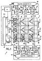
- Figure 1 shows the electrical diagram of a device photosensitive 1 according to the invention.
- the device photosensitive includes a plurality of photosensitive points P1, P2, ..., P9 which are arranged in rows and columns in a way by itself conventional, in order to constitute a photosensitive matrix 2.
- the number of photosensitive points P1 to P9 is limited to 9 depending on a 3x3 matrix assembly to simplify the figure 1, but in the spirit of the invention this assembly matrix can have much more capacity big.
- each photosensitive point P1 to P9 consists of two photosensitive cells JA, JB.
- Each photosensitive cell JA, JB has a photosensitive element DA, DB connected in series with a capacity CA, CB.
- the photosensitive device 1 further comprises conductors in lines L1 to L3 and, according to another characteristic of the invention, it comprises two networks FA, FB of conductors in columns FA1 to FA3 and FB1 to FB3.
- Line conductors L1 to L3 are connected to an addressing device 8, and the first and second FA, FB networks of column conductors are connected respectively to a first and a second device reading and multiplexing 9A, 9B.
- Cells photosensitive JA, JB have a first end 3A, 3B and a second end 4A, 4B by which these photosensitive cells are connected to line conductors L1 to L3 and to conductors columns FA1 to FA3 and FB1 to FB3.
- the two photosensitive cells JA, JB are connected by one end to the same conductor line, and are connected by the other end to column conductors of a different network.
- the first photosensitive point P1 has first and second cells JA, JB, the first ends of which 3A, 3B are gathered on the same first line L1.
- the second end 4A of the first JA photosensitive cell is joined to a column conductor FA1 of the first FA network, and the second end 4B of the second JB photosensitive cell is connected to a conductor column FB1 belonging to the second network FB.
- the first and second photosensitive cells JA, JB of the other photosensitive points P2 to P9 are similarly connected to line conductors L1 to L3 and aux column conductors FA1 to FA3 and FB1 to FB3, at the intersection which in practice is located the photosensitive point constituted by the two superimposed photosensitive cells JA, JB.
- the photosensitive elements DA, DB are photodiodes.
- Each photodiode is in series with a capacity CA, CB for constitute a photosensitive cell identical to cells photosensitive already described in patent applications French FR-A-2593319 and FR-A-2593343, previously cited, which describe in detail the operation of such cells photosensitive as well as the functioning of means useful for obtain the storage and reading of the charges or information; as a result these two patent applications (FR-A-2593319 and FR-A-2593343) should be considered as part of the present description.
- each point photosensitive P1 to P9 comprises two photosensitive cells JA, JB and therefore offers two pieces of information
- the operations above mentioned can be obtained in a way similar in principle to those described in the two above cited patent applications.
- the device addressing system includes a pulse generator 10 producing a pulsed voltage VL intended to be applied to line conductors L1 to L3.
- the generator pulse 3 is connected to the line conductors L1 to L3 by through MOS transistors M1, M2, M3, forming line switches controlled by outputs OL1, OL2, OL3 a shift register or line register 12.
- the line register 12 is controlled by an SCL shift control signal line. So conventionally, when a line of dots photosensitive P1 to P3, or P4 to P6 or P7 to P9 is selected, the corresponding line conductor L1 to L3 is connected to the pulse generator 10, so that the pulsed voltage VL is applied to all photosensitive points connected to it line conductor.
- each conductor line L1, L2, L3 is connected to ground by a resistor R1 to R3 ; these resistors R1 to R3 having a high value compared to the resistance presented by switches M1 to M3 when these the latter are closed (passing state).
- the column conductors FB1 to FB3 of the second FB network are connected in a similar way to integrating amplifiers GB1, GB2, GB3.
- these amplifier-integrators GB1 to GB3 each include a integration capacitor CL and a reset switch zero IB which are connected in parallel between the negative input "-" and the output OB1 to OB3 of these amplifier-integrators GB1 to GB3.
- the outputs OB1 to OB3 of these amplifier-integrators are connected respectively to the inputs EB1, EB2, EB3 of a second acquisition register 13 B, also consisting of a shift register of the type with parallel input and output S2 series.
- the matrix arrangement of the invention differs in what each photosensitive point P1 to P9 can store two different information, one at point A and the other at point B photosensitive cells JA, JB, so as to allow simultaneous acquisition of information relating to two images.
- the two photosensitive cells JA, JB are connected to the same driver online, and that on the other hand the first photosensitive cells A are connected to column conductors FA1 to FA3 different from the conductors columns FB1 to FB3 to which the second cells are connected photosensitive JB, operation at the level of one any of these JA or JB photosensitive cells, each consisting of a photosensitive element and a capacity series, basically remains the same as explained in the two patent applications mentioned above; the difference being that instead of having only signals of output relating to information stored at different first points A at output S1 of the first acquisition register 13A for example, one can also have, simultaneously or not, at output S2 of the second acquisition register 13B, signals relating to the information stored at the different second points B.
- Figure 2 shows the diagram of a second version of the photosensitive device 1 of the invention, in which at contrary to the example shown in Figure 1, the sense amplifiers are connected to line conductors L1 to L3.
- the photosensitive points P1 to P9 and the two cells photosensitive JA, JB which they each comprise are organized in the same way as in the first version.
- Each of these amplifier-integrators includes, as in the previous version, an integration capacitor CL and reset switch I which are connected in parallel, and which are connected on one side to its negative input "-", and the other side at its output OF1, OF2, OF3.
- the switches reset I are made up as in the previous example by MOS transistors, controlled by reset signals at zero V.RAZ.
- the second entry or positive entry "+" of each amplifier G1 to G3 is connected to ground, i.e. at the VCO column reference potential.
- the outputs OF1, OF2, OF3, amplifier-integrators G1 to G3 are connected to a third reading and multiplexing device or register analog data acquisition 74, consisting of a shift register of the type for example comprising a number n acquisition stages T1, T2 ..., Tn with parallel inputs E1, E2, ..., En and S serial output.
- a third reading and multiplexing device or register analog data acquisition 74 consisting of a shift register of the type for example comprising a number n acquisition stages T1, T2 ..., Tn with parallel inputs E1, E2, ..., En and S serial output.
- two acquisition stages are intended to be loaded successively by a same output OF1 to OF3 of amplifier G1 to G3.
- outputs OF1 OF2, OF3 are connected for example respectively at the second, fourth and sixth inputs E2, E4, E6 of acquisition register 74, so as to load in a first time the acquisition stages T2, T3, T4 by the charges or information contained in the first JA cells ( photosensitive points P1 to P9 connected to the same conductor line L1 to L3); then load the floors in a second step acquisition T1, T3, T5, by the information contained in the second JB cells, after having shifted the stages using an SD offset control signal applied to the third acquisition register 74.
- the column conductors FA1 to FA3 and FB1 to FB3 are all connected to the pulse generator 10 by through MOS transistors M4 to M9, forming column switches which are controlled by the outputs of two shift registers 15, 16 called column registers.
- the first column register 15 is controlled by a first signal SCA column command to successively render activates outputs OA1, OA2, OA3 which control respectively the first three column switches M4, M5, M6.
- the first three column switches M4, M5, M6 connect respectively to the pulse generator 10, the first, second and third column conductors FA1, FA2, FA3 of the first FA column network.
- the second register column 16 is controlled by a SCB column signal for successively rendering activate outputs OB1, OB2, OB3.
- OB1, OB2, OB3 outputs respectively control the column switches M7, M8, M9 which connect the first second and third respectively column conductors FB1, FB2, FB3 of the second column network FB.
- the first, fourth and seventh points photosensitive P1, P4, P7) are loaded into the amplifier-integrators G1, G2, G3 and transferred to the third acquisition register 74.
- a shift of the stages T1 to Tn of the third acquisition record 74 is then operated, in to allow the acquisition of the information contained in the point B of the same photosensitive points as above, that is, the first, fourth and seventh points photosensitive P1, P4, P7.
- the first OA1 output of the first column register 15 is deactivated, and this is the first output OB1 of the second column register 16 which is made active: switch M7 is then turned on and the pulse delivered by the generator 10 is then applied to the first column conductor FB1 of the second column network FB and as a result of the second JB photosensitive cells connected to this column conductor; as a result, the information stored at point B of the first, fourth and seventh points photosensitive P1, P4, P7 are in turn loaded into the third acquisition register 74. The latter is then emptied of its content for the benefit of the main memory previously mentioned.
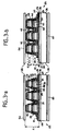
- Figures 3a and 3b are side sections along two orthogonal directions, which show as an example not limiting and schematically, an embodiment preferred of a dual energy radiological image detector, comprising a matrix device of photosensitive elements of the type previously described with reference to Figures 1 or 2.
- the image detector 25 includes a support or substrate 26, made of glass for example.
- a layer of a substance scintillator 27 is deposited on the substrate 26.
- This scintillating substance is chosen according to its maximum sensitivity in a certain energy range of the incident X-ray.
- gadolinium oxysulfide, terbium doped is known to have optimal sensitivity for X-rays whose energy is around 50 KeV, and to emit green wavelength light in response O, 54 microns.
- the scintillator layer 27 may consist of gadolinium oxysulfide powder embedded in a thermosetting resin, so constitute a leaf. This sheet is then stuck on the substrate 26.
- the scintillator layer 27 has a thickness which is chosen to optimize the efficiency of photon production, without losing too much on the resolution; this thickness (no illustrated) can range from a few tens to a few hundred microns for radiological imaging applications.
- the thin conductive layer 28 can be example of indium tin oxide, and it is engraved so that constitute column conductors, for example column conductors FB1 to FB3 of the second column network FB.
- the insulating layer 34 intended to form the dielectric of second CB capacities.
- the insulating layer 34 which forms the dielectric is also transparent, and it is made up for example made of silicon nitride.
- the dielectric layer 34 is in turn covered by a stack of several layers 30, 31, 32 which after etching constitute the second DB photodiodes previously mentioned.
- the second DB photodiodes are of the NIP type, i.e. on the layer insulator 34 (intended to form a dielectric), there are first layer 30 of hydrogenated amorphous silicon, doped with an N-type impurity of phosphorus for example.
- the layer 31 in intrinsic hydrogenated amorphous silicon is deposited on the layer 31 of intrinsic silicon, a layer of amorphous hydrogenated silicon 32, doped with an impurity of the type P, for example boron.
- These last three layers 30, 31, 32 are engraved according to a pattern of islands so as to constitute the second DB photodiodes; these second DB photodiodes in island form are thus located at each of the points of crossing between conductors in column FA1 to FA3 and FB1 to FB3 and line conductors L1 to L3.
- a new insulating layer 29 is deposited, which can be made for example of the same material as the layer insulator 34 which forms the dielectric of the second capacitors CB. Openings are made in this last layer insulator 29, above the second photodiodes DB, so that put these in contact with a layer of material conductor called intermediate conductive layer 51, and which is engraved to constitute the conductors in lines L1 to L3.
- the conductive intermediate layer 51 can be opaque, constituted for example by a deposit of chromium or molybdenum. But, if the upgrade is done optically, the conductive intermediate layer 51 must be transparent, in the same material for example as the layer conductor 28 forming the column conductors FB1 to FB3.
- these three successive layers 40, 41, 42 being respectively a doped hydrogenated amorphous silicon layer with a P-type impurity, a layer of amorphous silicon intrinsic hydrogné, a layer of hydrogenated amorphous silicon doped with an N-type impurity (phosphorus for example).
- These last three layers 40, 41, 42 are etched according to a island pattern so as to constitute the first DA photodiodes superimposed on the second DB photodiodes.
- the first DA photodiodes is realized depositing an insulating layer 55 which constitutes the dielectric of the first CA capacities.
- an upper conductive layer 56 transparent, made for example of the same material conductor than the layer 28 with which the column conductors FB1 to FB3 belonging to the second network column FB.
- This upper conductive layer 56 is etched so as to constitute the column conductors FA1 to FA3 of the first FA column network.
- a second layer of a scintillating substance 58 completes the structure, and covers the upper conductive layer 56 on which it is glued or pressed with a transparent link (not shown) in the light.
- the scintillating substance that forms the second scintillator layer 58 is chosen according to the range of X-ray energy for which it has a maximum sensitivity, this maximum sensitivity being presented of course for a range of X-ray energy different from that of the first scintillating layer 27.
- this may consist of oxide yttrium so as to present an optimal sensitivity for 20 Kev x-rays.
- Second layer yttrium oxide scintillator 58 which can be doped for example with terbium.
- the points photosensitive of the matrix device are produced by superimposed layers, stacked in the direction of a thickness E of the structure, so that for the same photosensitive point the two photosensitive cells JA, JB which constitute it, and particularly the first and second photodiodes DA, DB are perfectly superimposed. So for each point photosensitive, the lateral dimensions are minimal, so that photodiodes DA, DB can have a detector surface as large as possible.
- This structure is advantageous in addition to the fact that the first and second photodiodes DA, DB must be sensitive to (light) radiation of different origin, which is achieved by sandwiching between the two scintillating layers 27, 58 the different overlapping layers which constitute the first and second photosensitive cells JA, JB.
- the first SA scintillator mainly absorbs X-rays with an energy range centered around 20 KeV for example and it converts the x-rays that it absorbs into a radiation detectable by amorphous silicon.
- the second scintillator SB mainly absorbs X-rays including the energy corresponds to its maximum sensitivity which is located at energies (50 KeV for example) different than in the case of first SA scintillator, the absorbed X-rays also being converted into radiation detectable by amorphous silicon.
- the first DA photodiodes located near the first SA scintillator preferentially capture light emitted by the first SA scintillator
- the seconds photodiodes DB located near the second scintillator SB preferentially capture the light emitted by this second scintillator; each photodiode constituting a screen between the other photodiode on which it is superimposed and the scintillator near which it is located.
- amorphous silicon for example radiation and in particular the light emitted by the scintillating layers SA, SB is absorbed or attenuated in photosensitive matter in such a way that the energy given up to this material decreases exponentially with the length of material crossed. It follows that if the first and the second photodiodes DA, DB have thicknesses E1, E2 similar, the light emitted by the first layer scintillatrice SA is absorbed and therefore detected essentially by the first DA photodiodes; and that the light emitted by the second scintillating layer SB is absorbed and detected essentially by the second photodiodes DB.
- the thicknesses E1, E2 of the photodiodes DA, DB are sufficient to fully absorb the radiation or light emitted by the scintillating layer which is the closest, we get a total separation between the information provided by the first scintillating layer SA and the information provided by the second scintillator layer SB, this information being detected respectively by the first and second photodiodes DA and DB.
- a such separation is only useful if the conductive layer intermediate 51 in which the conductors are made line, is transparent.
- a refresher (RAN) of the type optical which can be performed simultaneously for both photodiodes DA, DB of the same photosensitive point and possibly for all photosensitive points, from of light emitted by a single light source.
- a light source 60 intended for a general leveling, can be pressed against the substrate 26, for example opposite the second scintillator SB.
- This light source 60 can be formed by means in them same known, for example by a lumiplaque, or by a network of light-emitting diodes, or by tubes with shine, etc ....
- the substrate 26 must then itself be transparent. A classic substrate glass fits perfectly.
- the light source 60 can then be constituted by a network of diodes electroluminescent (not shown) mounted so as to form a panel, as in the example described in a French patent application FR-A-2598250.
- the latter emits a red light, that is to say a light of wavelength greater than the light emitted by the scintillators SA, SB; this tends to decrease the absorption of light used for leveling general with respect to the absorption of light emitted by scintillators SA, SB.
- the intermediate conductive layer 51 which constitutes the line conductors located between the first and the second photosensitive cells JA, JB, is opaque and does not not let visible light (or near visible light) through, it is preferably by electrical impulses that upgraded the DA, DB photodiodes.
- FIG. 3a, 3b is given by way of nonlimiting example, and in particular the layers with which the first and second photosensitive cells JA, JB can be arranged in different orders, so as to constitute for example PIN or PIN type photodiodes, or so as to modify the positions between the photodiode and the capacity of the same cell photosensitive.
- the elements photosensitive DA, DB can consist of NIPIN or PINIP type phototransistors.
Landscapes
- Engineering & Computer Science (AREA)
- Multimedia (AREA)
- Signal Processing (AREA)
- Measurement Of Radiation (AREA)
- Solid State Image Pick-Up Elements (AREA)
- Transforming Light Signals Into Electric Signals (AREA)
Claims (14)
- Bilddetektor mit einer Matrix aus photoempfindlichen Punkten (P1 bis P9), welche photoempfindlichen Punkte mit Zeilenleitern (L1 bis L3) und Spaltenleitern (FA1 bis FA3, FB1 bis FB3) verbunden sind, wobei jeder photoempfindliche Punkt eine erste und eine zweite photoempfindliche Zelle (JA, JB) aufweist, von denen jede dazu in der Lage ist, Information zu speichern, wobei die zwei Zellen übereinander angeordnet sind, dadurch gekennzeichnet, daß er zwei szintillierende Schichten (SA, SB) aufweist, die für verschiedene Energien einfallender Strahlung empfindlich sind, und daß die Matrix aus photoempfindlichen Punkten aus einem Stapel von Schichten besteht, der zwischen den zwei szintillierenden Schichten angeordnet ist, wobei das Ganze auf eine Substratsfläche aufgebracht ist.
- Bilddetektor nach Anspruch 1, dadurch gekennzeichnet, daß die Spaltenleiter (FA1 bis FA3, FB1 bis FB3) in zwei Gitter (FA, FB) unterteilt sind und daß die erste und die zweite photoempfindliche Zelle (JA, JB) eines jeweiligen photoempfindlichen Punktes (P1 bis P9) mit ihrem ersten Ende (3A, 3B) mit demselben einen Zeilenleiter (L1 bis L3) verbunden sind und mit ihrem zweiten Anschluß (4A, 4B) mit einem Spaltenleiter (FA1 bis FA3, FB1 bis FB3) eines anderen Spaltengitters (FA, FB) verbunden sind.
- Bilddetektor nach einem der vorstehenden Ansprüche, dadurch gekennzeichnet, daß jede photoempfindliche Zelle (JA, JB) durch ein photoempfindliches Element (DA, DB) gebildet wird, das in Reihe mit einer Kapazität (CA, CB) liegt.
- Bilddetektor nach Anspruch 3, dadurch gekennzeichnet, daß die photoempfindlichen Elemente (DA, DB) Photodioden sind.
- Bilddetektor nach Anspruch 3, dadurch gekennzeichnet, daß die photoempfindlichen Elemente (DA, DB) Phototransistoren vom NIPIN- oder PINIP-Typ sind.
- Bilddetektor nach einem der vorstehenden Ansprüche, dadurch gekennzeichnet, daß die Zeilenleiter (LA1 bis LA3) mit einer Adressiervorrichtung (8) verbunden sind und daß einerseits die Spaltenleiter (FA1 bis FA3) des ersten Spaltengitters (FA) mit einer ersten Vorrichtung für Lesen und Multiplexen (9A) verbunden sind und daß andererseits die Spaltenleiter (FB1 bis FB3) des zweiten Spaltengitters (FB) mit einer zweiten Vorrichtung zum Lesen und Multiplexen (9B) verbunden sind.
- Bilddetektor nach einem der Ansprüche 1 bis 5, dadurch gekennzeichnet, daß die Zeilenleiter (L1 bis L3) mit einer Vorrichtung zum Lesen und Multiplexen (74) verbunden sind und daß das erste und das zweite Gitter (FA, FB) der Spaltenleiter (FA1 bis FA3, FB1 bis FB3) jeweils mit einer Adressiervorrichtung verbunden sind (8A, 8B).
- Bilddetektor nach einem der vorstehenden Ansprüche, dadurch gekennzeichnet, daß die ersten und die zweiten photoempfindlichen Zellen (JA, JB) von einem Substrat (26) getragen werden und jeweils ausgehend von einem Stapel halbleitender Schichten (30, 31, 32 und 40, 41, 42) und einer isolierenden Schicht (34, 55) gebildet werden, wobei all diese Schichten zwischen zwei leitenden Schichten (28, 58) übereinander angeordnet sind, von denen die eine so geätzt ist, daß sie Spaltenleiter (FB1 bis FB3) des zweiten Spaltengitters (FB) bildet, und die andere so geätzt ist, daß sie Spaltenleiter (FA1 bis FA3) des ersten Spaltengitters (FA) bildet, und daß die zwei Stapel oder Zellen (JA, JB) durch eine leitende Zwischenschicht (51) voneinander getrennt werden, mit der die Zeilenleiter (L1 bis L3) realisiert sind.
- Bilddetektor nach Anspruch 8, dadurch gekennzeichnet, daß die leitende Zwischenschicht (51) lichtdurchlässig ist.
- Bilddetektor nach Anspruch 9, dadurch gekennzeichnet, daß die photoempfindlichen Elemente (DA, DB) im wesentlichen gleiche Dicken (E1, E2) aufweisen.
- Bilddetektor nach einem der Ansprüche 9 oder 10, dadurch gekennzeichnet, daß er ferner eine Lichtquelle (60) aufweist, die es erlaubt, eine Pegelrückstellung an den Anschlüssen der photoempfindlichen Elemente (DA, DB) vorzunehmen.
- Bildetektor nach Anspruch 8, dadurch gekennzeichnet, daß die leitende Zwischenschicht (51) lichtundurchlässig ist.
- Bilddetektor nach Anspruch 11, dadurch gekennzeichnet, daß die Lichtquelle (60) Licht einer Wellenlänge aufweist, die größer ist als diejenige des von den szintillierenden Schichten (SA, SB) emittierten Lichts.
- Bilddetektor nach einem der vorstehenden Ansprüche, dadurch gekennzeichnet, daß die auftreffende Strahlung Röntgenstrahlung ist.
Applications Claiming Priority (2)
| Application Number | Priority Date | Filing Date | Title |
|---|---|---|---|
| FR8802366 | 1988-02-26 | ||
| FR8802366A FR2627924B1 (fr) | 1988-02-26 | 1988-02-26 | Dispositif photosensible et detecteur d'images comportant un tel dispositif, notamment detecteur d'images a double energie |
Publications (3)
| Publication Number | Publication Date |
|---|---|
| EP0333533A1 EP0333533A1 (de) | 1989-09-20 |
| EP0333533B1 EP0333533B1 (de) | 1993-04-07 |
| EP0333533B2 true EP0333533B2 (de) | 2000-04-26 |
Family
ID=9363664
Family Applications (1)
| Application Number | Title | Priority Date | Filing Date |
|---|---|---|---|
| EP89400480A Expired - Lifetime EP0333533B2 (de) | 1988-02-26 | 1989-02-21 | Photoempfindliche Einrichtung und Bildsensor mit einer solchen Einrichtung, insbesondere Doppel-Energie-Bildsensor |
Country Status (4)
| Country | Link |
|---|---|
| US (1) | US4945242A (de) |
| EP (1) | EP0333533B2 (de) |
| DE (1) | DE68905851T3 (de) |
| FR (1) | FR2627924B1 (de) |
Families Citing this family (90)
| Publication number | Priority date | Publication date | Assignee | Title |
|---|---|---|---|---|
| JPH06205767A (ja) * | 1992-11-25 | 1994-07-26 | Xerox Corp | 放射線画像形成システム |
| GB9301405D0 (en) * | 1993-01-25 | 1993-03-17 | Philips Electronics Uk Ltd | An image sensor |
| GB9308543D0 (en) * | 1993-04-24 | 1993-06-09 | Philips Electronics Uk Ltd | An image sensor |
| WO1994025878A1 (en) * | 1993-04-28 | 1994-11-10 | University Of Surrey | Radiation detectors |
| GB9313841D0 (en) * | 1993-07-05 | 1993-08-18 | Philips Electronics Uk Ltd | An electro-optic device |
| GB9314402D0 (en) * | 1993-07-12 | 1993-08-25 | Philips Electronics Uk Ltd | An imaging device |
| DE4429434C1 (de) * | 1994-08-19 | 1995-12-21 | Siemens Ag | Bildsensor |
| US5561287A (en) * | 1994-09-30 | 1996-10-01 | Board Of Regents Of The University Of Colorado | Dual photodetector for determining peak intensity of pixels in an array using a winner take all photodiode intensity circuit and a lateral effect transistor pad position circuit |
| FR2731569B1 (fr) * | 1995-03-07 | 1997-04-25 | Thomson Tubes Electroniques | Dispositif de recopie de tension a grande linearite |
| DE69833848T2 (de) * | 1997-01-06 | 2006-11-23 | Philips Intellectual Property & Standards Gmbh | Vorrichtung zum auslesen einer bildsensormatrix |
| US6491394B1 (en) | 1999-07-02 | 2002-12-10 | E-Vision, Llc | Method for refracting and dispensing electro-active spectacles |
| US6733130B2 (en) | 1999-07-02 | 2004-05-11 | E-Vision, Llc | Method for refracting and dispensing electro-active spectacles |
| US6517203B1 (en) | 1999-07-02 | 2003-02-11 | E-Vision, Llc | System, apparatus, and method for correcting vision using electro-active spectacles |
| US6491391B1 (en) | 1999-07-02 | 2002-12-10 | E-Vision Llc | System, apparatus, and method for reducing birefringence |
| US7023594B2 (en) | 2000-06-23 | 2006-04-04 | E-Vision, Llc | Electro-optic lens with integrated components |
| US6871951B2 (en) | 2000-06-23 | 2005-03-29 | E-Vision, Llc | Electro-optic lens with integrated components |
| US6857741B2 (en) * | 2002-01-16 | 2005-02-22 | E-Vision, Llc | Electro-active multi-focal spectacle lens |
| US6986579B2 (en) * | 1999-07-02 | 2006-01-17 | E-Vision, Llc | Method of manufacturing an electro-active lens |
| US6619799B1 (en) * | 1999-07-02 | 2003-09-16 | E-Vision, Llc | Optical lens system with electro-active lens having alterably different focal lengths |
| US20070258039A1 (en) * | 1999-07-02 | 2007-11-08 | Duston Dwight P | Spectacle frame bridge housing electronics for electro-active spectacle lenses |
| US7290875B2 (en) * | 2004-11-02 | 2007-11-06 | Blum Ronald D | Electro-active spectacles and method of fabricating same |
| US7775660B2 (en) * | 1999-07-02 | 2010-08-17 | E-Vision Llc | Electro-active ophthalmic lens having an optical power blending region |
| US7604349B2 (en) * | 1999-07-02 | 2009-10-20 | E-Vision, Llc | Static progressive surface region in optical communication with a dynamic optic |
| US6851805B2 (en) * | 1999-07-02 | 2005-02-08 | E-Vision, Llc | Stabilized electro-active contact lens |
| US7404636B2 (en) | 1999-07-02 | 2008-07-29 | E-Vision, Llc | Electro-active spectacle employing modal liquid crystal lenses |
| US7290876B2 (en) * | 1999-07-02 | 2007-11-06 | E-Vision, Llc | Method and system for electro-active spectacle lens design |
| US7988286B2 (en) | 1999-07-02 | 2011-08-02 | E-Vision Llc | Static progressive surface region in optical communication with a dynamic optic |
| US20090103044A1 (en) * | 1999-07-02 | 2009-04-23 | Duston Dwight P | Spectacle frame bridge housing electronics for electro-active spectacle lenses |
| US7264354B2 (en) * | 1999-07-02 | 2007-09-04 | E-Vision, Llc | Method and apparatus for correcting vision using an electro-active phoropter |
| DE10034575A1 (de) * | 2000-07-14 | 2002-01-24 | Philips Corp Intellectual Pty | Röntgendetektor mit verbesserter Lichtausbeute |
| EP1433020A1 (de) * | 2001-10-05 | 2004-06-30 | E-Vision, LLC | Hybride elektroaktive linse |
| AR045370A1 (es) | 2003-08-15 | 2005-10-26 | E Vision Llc | Sistema de lente electro-activo |
| US7045760B2 (en) * | 2003-12-19 | 2006-05-16 | Searete Llc | Intensity detector circuitry |
| US7999214B2 (en) * | 2003-12-19 | 2011-08-16 | The Invention Science Fund I, Llc | Photo-detector filter having a cascaded low noise amplifier |
| US7053998B2 (en) * | 2003-12-22 | 2006-05-30 | Searete Llc | Photo-detector filter |
| US7515082B2 (en) * | 2003-12-19 | 2009-04-07 | Searete, Llc | Photo-detector filter having a cascaded low noise amplifier |
| US7511254B2 (en) * | 2003-12-19 | 2009-03-31 | Searete, Llc | Photo-detector filter having a cascaded low noise amplifier |
| US7250595B2 (en) * | 2004-01-14 | 2007-07-31 | Searete, Llc | Photo-detector filter having a cascaded low noise amplifier |
| US7053809B2 (en) * | 2003-12-19 | 2006-05-30 | Searete Llc | Analog-to-digital converter circuitry having a cascade |
| US7542133B2 (en) * | 2003-12-22 | 2009-06-02 | Searete, Llc | Photo-detector filter |
| CN101057174A (zh) * | 2004-04-13 | 2007-10-17 | 庄臣及庄臣视力保护公司 | 用于电活性液晶眼科设备的图案化电极 |
| US20050237485A1 (en) * | 2004-04-21 | 2005-10-27 | Blum Ronald D | Method and apparatus for correcting vision |
| JP4385844B2 (ja) * | 2004-04-23 | 2009-12-16 | ソニー株式会社 | 固体撮像装置および固体撮像装置の駆動方法 |
| DE102004026842B4 (de) * | 2004-06-02 | 2007-12-27 | Siemens Ag | Röntgendetektor |
| US20060067472A1 (en) * | 2004-09-30 | 2006-03-30 | Possin George E | Method and apparatus for measuring X-ray energy |
| US8915588B2 (en) | 2004-11-02 | 2014-12-23 | E-Vision Smart Optics, Inc. | Eyewear including a heads up display |
| US8778022B2 (en) | 2004-11-02 | 2014-07-15 | E-Vision Smart Optics Inc. | Electro-active intraocular lenses |
| MX2007005198A (es) * | 2004-11-02 | 2007-06-20 | E Vision Llc | Anteojos electro-activos y metodos para fabricarlos. |
| US9801709B2 (en) | 2004-11-02 | 2017-10-31 | E-Vision Smart Optics, Inc. | Electro-active intraocular lenses |
| US7656569B2 (en) | 2004-12-03 | 2010-02-02 | Searete Llc | Vision modification with reflected image |
| US7344244B2 (en) | 2004-12-03 | 2008-03-18 | Searete, Llc | Adjustable lens system with neural-based control |
| US9155483B2 (en) | 2004-12-03 | 2015-10-13 | The Invention Science Fund I, Llc | Vision modification with reflected image |
| US7350919B2 (en) * | 2004-12-03 | 2008-04-01 | Searete Llc | Vision modification with reflected image |
| US7390088B2 (en) * | 2004-12-03 | 2008-06-24 | Searete Llc | Adjustable lens system with neural-based control |
| US7931373B2 (en) | 2004-12-03 | 2011-04-26 | The Invention Science Fund I, Llc | Vision modification with reflected image |
| US7334892B2 (en) * | 2004-12-03 | 2008-02-26 | Searete Llc | Method and system for vision enhancement |
| US7470027B2 (en) * | 2004-12-03 | 2008-12-30 | Searete Llc | Temporal vision modification |
| US8244342B2 (en) | 2004-12-03 | 2012-08-14 | The Invention Science Fund I, Llc | Method and system for adaptive vision modification |
| US8104892B2 (en) | 2004-12-03 | 2012-01-31 | The Invention Science Fund I, Llc | Vision modification with reflected image |
| US7486988B2 (en) * | 2004-12-03 | 2009-02-03 | Searete Llc | Method and system for adaptive vision modification |
| US7594727B2 (en) * | 2004-12-03 | 2009-09-29 | Searete Llc | Vision modification with reflected image |
| US7334894B2 (en) * | 2004-12-03 | 2008-02-26 | Searete, Llc | Temporal vision modification |
| US20070159562A1 (en) * | 2006-01-10 | 2007-07-12 | Haddock Joshua N | Device and method for manufacturing an electro-active spectacle lens involving a mechanically flexible integration insert |
| US20080273166A1 (en) * | 2007-05-04 | 2008-11-06 | William Kokonaski | Electronic eyeglass frame |
| US7656509B2 (en) | 2006-05-24 | 2010-02-02 | Pixeloptics, Inc. | Optical rangefinder for an electro-active lens |
| JP2009541793A (ja) | 2006-06-23 | 2009-11-26 | ピクセルオプティクス, インコーポレイテッド | 電気活性眼鏡レンズ用の電子アダプタ |
| EP2082281A4 (de) * | 2006-10-27 | 2010-03-10 | Pixeloptics Inc | Brillenbügel für brillengläser |
| AR064985A1 (es) | 2007-01-22 | 2009-05-06 | E Vision Llc | Lente electroactivo flexible |
| MX2009008829A (es) | 2007-02-23 | 2011-10-28 | Pixeloptics Inc | Apertura dinamica oftalmica. |
| CA2679977A1 (en) | 2007-03-07 | 2008-09-18 | Pixeloptics, Inc. | Multifocal lens having a progressive optical power region and a discontinuity |
| US20080273169A1 (en) | 2007-03-29 | 2008-11-06 | Blum Ronald D | Multifocal Lens Having a Progressive Optical Power Region and a Discontinuity |
| US7883207B2 (en) | 2007-12-14 | 2011-02-08 | Pixeloptics, Inc. | Refractive-diffractive multifocal lens |
| JP4790863B2 (ja) * | 2007-04-23 | 2011-10-12 | コーニンクレッカ フィリップス エレクトロニクス エヌ ヴィ | 部分的に透明なシンチレータ基板を有する検出器、検査装置及びその製造方法 |
| US11061252B2 (en) | 2007-05-04 | 2021-07-13 | E-Vision, Llc | Hinge for electronic spectacles |
| US10613355B2 (en) | 2007-05-04 | 2020-04-07 | E-Vision, Llc | Moisture-resistant eye wear |
| US12572035B2 (en) | 2007-05-04 | 2026-03-10 | E-Vision Optics, Llc | Moisture-resistant eye wear |
| US8317321B2 (en) * | 2007-07-03 | 2012-11-27 | Pixeloptics, Inc. | Multifocal lens with a diffractive optical power region |
| CN101911780B (zh) * | 2008-01-09 | 2014-08-13 | 皇家飞利浦电子股份有限公司 | 在使用定向天线的无线网络中进行无线设备发现的方法和系统 |
| BRPI0908992A2 (pt) | 2008-03-18 | 2015-11-24 | Pixeloptics Inc | dispositivo ótico eletro-ativo avançado |
| US8154804B2 (en) | 2008-03-25 | 2012-04-10 | E-Vision Smart Optics, Inc. | Electro-optic lenses for correction of higher order aberrations |
| DE102008021170B4 (de) | 2008-04-28 | 2010-02-11 | Siemens Aktiengesellschaft | Vorrichtung zur Aufnahme von Signalen |
| JP5374110B2 (ja) * | 2008-10-22 | 2013-12-25 | キヤノン株式会社 | 撮像センサ及び撮像装置 |
| US12436411B2 (en) | 2010-07-02 | 2025-10-07 | E-Vision Optics, Llc | Moisture-resistant eye wear |
| US12510773B2 (en) | 2011-02-11 | 2025-12-30 | E-Vision Optics, Llc | Moisture-resistant eye wear |
| CA3167661A1 (en) | 2012-01-06 | 2013-07-11 | E-Vision Smart Optics, Inc. | Eyewear docking station and electronic module |
| US20160003672A1 (en) * | 2014-07-25 | 2016-01-07 | Varun Verma | Multiplexer for single photon detector, process for making and use of same |
| ES2861520T3 (es) | 2016-04-12 | 2021-10-06 | E Vision Smart Optics Inc | Lentes electroactivas con puentes resistivos elevados |
| US10599006B2 (en) | 2016-04-12 | 2020-03-24 | E-Vision Smart Optics, Inc. | Electro-active lenses with raised resistive bridges |
| JP2021076393A (ja) * | 2019-11-05 | 2021-05-20 | キヤノン株式会社 | 放射線撮像装置及び放射線撮像システム |
| FR3119708B1 (fr) * | 2021-02-11 | 2023-08-25 | Trixell | Détecteur numérique à étages de conversion superposés |
Family Cites Families (5)
| Publication number | Priority date | Publication date | Assignee | Title |
|---|---|---|---|---|
| US3660667A (en) * | 1970-06-22 | 1972-05-02 | Rca Corp | Image sensor array in which each element employs two phototransistors one of which stores charge |
| US4581625A (en) * | 1983-12-19 | 1986-04-08 | Atlantic Richfield Company | Vertically integrated solid state color imager |
| US4672454A (en) * | 1984-05-04 | 1987-06-09 | Energy Conversion Devices, Inc. | X-ray image scanner and method |
| US4789930A (en) * | 1985-11-15 | 1988-12-06 | Picker International, Inc. | Energy dependent gain correction for radiation detection |
| FR2593343B1 (fr) * | 1986-01-20 | 1988-03-25 | Thomson Csf | Matrice d'elements photosensibles et son procede de fabrication, procede de lecture associe, et application de cette matrice a la prise de vue d'images |
-
1988
- 1988-02-26 FR FR8802366A patent/FR2627924B1/fr not_active Expired - Lifetime
-
1989
- 1989-02-21 DE DE68905851T patent/DE68905851T3/de not_active Expired - Fee Related
- 1989-02-21 EP EP89400480A patent/EP0333533B2/de not_active Expired - Lifetime
- 1989-02-22 US US07/314,435 patent/US4945242A/en not_active Expired - Lifetime
Also Published As
| Publication number | Publication date |
|---|---|
| DE68905851D1 (de) | 1993-05-13 |
| FR2627924A1 (fr) | 1989-09-01 |
| EP0333533A1 (de) | 1989-09-20 |
| DE68905851T3 (de) | 2000-10-26 |
| FR2627924B1 (fr) | 1990-06-22 |
| EP0333533B1 (de) | 1993-04-07 |
| DE68905851T2 (de) | 1993-07-15 |
| US4945242A (en) | 1990-07-31 |
Similar Documents
| Publication | Publication Date | Title |
|---|---|---|
| EP0333533B2 (de) | Photoempfindliche Einrichtung und Bildsensor mit einer solchen Einrichtung, insbesondere Doppel-Energie-Bildsensor | |
| FR2627923A1 (fr) | Matrice d'elements photosensibles et detecteur de radiations comportant une telle matrice, notamment detecteur de rayons x a double energie | |
| EP0316222B1 (de) | Röntgen-Bildaufnehmer | |
| EP0362352B1 (de) | Belegleser | |
| EP0245147A1 (de) | Röntgen-Bilderfassungstafel und deren Herstellungsverfahren | |
| US5381014A (en) | Large area X-ray imager and method of fabrication | |
| EP1378113B1 (de) | Photoempfindliche vorrichtung und verfahren zur steuerung der photoempfindlichen vorrichtung | |
| EP2564239B1 (de) | Detektor elektromagnetischer strahlung mit verstärkungsbereichauswahl | |
| EP0337826A1 (de) | Strahlungsdtektor in Matrix-Anordnung | |
| EP0341121A1 (de) | Röntgenbilddetektor | |
| JPS60240285A (ja) | 電子的輻射感知装置及び方法 | |
| EP3069506B1 (de) | Pooling von zwei pixelspalten eines bilddetektors | |
| EP0324677B1 (de) | Photoempfindliche Matrix mit drei Dioden pro Punkt ohne Rückstellung | |
| EP0316221A1 (de) | Matrix aus photoempfindlichen Elementen, die je aus einem Phototransistor und einem Speicherkondensator bestehen | |
| EP0331546A1 (de) | Photoempfindlicher Matrix mit zwei Dioden pro Punkt ohne spezifischen Rückstellungsleiter | |
| FR2849273A1 (fr) | Matrice de detecteurs multispectraux | |
| EP0357468B1 (de) | Photoempfindliche Matrix mit zwei Dioden gleicher Polarität und einer Kapazität pro photoempfindlichem Punkt | |
| EP0378593A1 (de) | Anzeige- und schreibanordnung | |
| EP0324678A1 (de) | Photoempfindliche Matrix mit zwei Dioden und einer Kapazität pro Punkt ohne optische Rückstellung | |
| FR2758654A1 (fr) | Procede de realisation d'un detecteur de rayonnement a ecran plat et detecteur obtenu par ce procede | |
| EP0319403A1 (de) | Matrix photoempfindlicher Elemente, die je eine Diode oder eine Diode und einen Speicherkondensator enthalten | |
| JPH02253185A (ja) | 感光素子のマトリックス及びマトリックスを含む放射線検出器 | |
| JP2923965B2 (ja) | イメージ検出器 | |
| FR2758655A1 (fr) | Procede de realisation d'un detecteur de radiographie par assemblage de dalles elementaires et detecteur ainsi obtenu | |
| FR3125891A1 (fr) | Détecteur photosensible matriciel et procédé de réalisation du détecteur photosensible |
Legal Events
| Date | Code | Title | Description |
|---|---|---|---|
| PUAI | Public reference made under article 153(3) epc to a published international application that has entered the european phase |
Free format text: ORIGINAL CODE: 0009012 |
|
| AK | Designated contracting states |
Kind code of ref document: A1 Designated state(s): DE FR GB NL |
|
| 17P | Request for examination filed |
Effective date: 19891219 |
|
| 17Q | First examination report despatched |
Effective date: 19920320 |
|
| GRAA | (expected) grant |
Free format text: ORIGINAL CODE: 0009210 |
|
| AK | Designated contracting states |
Kind code of ref document: B1 Designated state(s): DE FR GB NL |
|
| REF | Corresponds to: |
Ref document number: 68905851 Country of ref document: DE Date of ref document: 19930513 |
|
| GBT | Gb: translation of ep patent filed (gb section 77(6)(a)/1977) |
Effective date: 19930524 |
|
| PLBI | Opposition filed |
Free format text: ORIGINAL CODE: 0009260 |
|
| RAP2 | Party data changed (patent owner data changed or rights of a patent transferred) |
Owner name: THOMSON-CSF |
|
| 26 | Opposition filed |
Opponent name: PHILIPS ELECTRONICS N.V. Effective date: 19940107 |
|
| NLT2 | Nl: modifications (of names), taken from the european patent patent bulletin |
Owner name: THOMSON-CSF TE PARIJS, FRANKRIJK. |
|
| NLR1 | Nl: opposition has been filed with the epo |
Opponent name: PHILIPS ELECTRONICS N.V. |
|
| PLAW | Interlocutory decision in opposition |
Free format text: ORIGINAL CODE: EPIDOS IDOP |
|
| PLAW | Interlocutory decision in opposition |
Free format text: ORIGINAL CODE: EPIDOS IDOP |
|
| PUAH | Patent maintained in amended form |
Free format text: ORIGINAL CODE: 0009272 |
|
| STAA | Information on the status of an ep patent application or granted ep patent |
Free format text: STATUS: PATENT MAINTAINED AS AMENDED |
|
| 27A | Patent maintained in amended form |
Effective date: 20000426 |
|
| AK | Designated contracting states |
Kind code of ref document: B2 Designated state(s): DE FR GB NL |
|
| NLR2 | Nl: decision of opposition | ||
| GBTA | Gb: translation of amended ep patent filed (gb section 77(6)(b)/1977) | ||
| NLR3 | Nl: receipt of modified translations in the netherlands language after an opposition procedure | ||
| REG | Reference to a national code |
Ref country code: GB Ref legal event code: IF02 |
|
| PGFP | Annual fee paid to national office [announced via postgrant information from national office to epo] |
Ref country code: GB Payment date: 20030219 Year of fee payment: 15 |
|
| PGFP | Annual fee paid to national office [announced via postgrant information from national office to epo] |
Ref country code: NL Payment date: 20030226 Year of fee payment: 15 |
|
| PGFP | Annual fee paid to national office [announced via postgrant information from national office to epo] |
Ref country code: DE Payment date: 20030306 Year of fee payment: 15 |
|
| PG25 | Lapsed in a contracting state [announced via postgrant information from national office to epo] |
Ref country code: GB Free format text: LAPSE BECAUSE OF NON-PAYMENT OF DUE FEES Effective date: 20040221 |
|
| PG25 | Lapsed in a contracting state [announced via postgrant information from national office to epo] |
Ref country code: NL Free format text: LAPSE BECAUSE OF NON-PAYMENT OF DUE FEES Effective date: 20040901 Ref country code: DE Free format text: LAPSE BECAUSE OF NON-PAYMENT OF DUE FEES Effective date: 20040901 |
|
| GBPC | Gb: european patent ceased through non-payment of renewal fee |
Effective date: 20040221 |
|
| NLV4 | Nl: lapsed or anulled due to non-payment of the annual fee |
Effective date: 20040901 |
|
| PGFP | Annual fee paid to national office [announced via postgrant information from national office to epo] |
Ref country code: FR Payment date: 20080208 Year of fee payment: 20 |
|
| PLAB | Opposition data, opponent's data or that of the opponent's representative modified |
Free format text: ORIGINAL CODE: 0009299OPPO |