EP0334273A2 - Befestigungsanordnung für das Messen der statischen Charakteristika von aktiven Mikrowellenkomponenten mit 3 Anschlüssen - Google Patents
Befestigungsanordnung für das Messen der statischen Charakteristika von aktiven Mikrowellenkomponenten mit 3 Anschlüssen Download PDFInfo
- Publication number
- EP0334273A2 EP0334273A2 EP89104997A EP89104997A EP0334273A2 EP 0334273 A2 EP0334273 A2 EP 0334273A2 EP 89104997 A EP89104997 A EP 89104997A EP 89104997 A EP89104997 A EP 89104997A EP 0334273 A2 EP0334273 A2 EP 0334273A2
- Authority
- EP
- European Patent Office
- Prior art keywords
- component
- fixture
- dielectric substrates
- lines
- supporting
- Prior art date
- Legal status (The legal status is an assumption and is not a legal conclusion. Google has not performed a legal analysis and makes no representation as to the accuracy of the status listed.)
- Granted
Links
- 230000003068 static effect Effects 0.000 title claims abstract description 8
- 239000000758 substrate Substances 0.000 claims abstract description 20
- 239000003990 capacitor Substances 0.000 claims description 5
- 239000000463 material Substances 0.000 claims description 5
- 239000004020 conductor Substances 0.000 claims description 2
- 238000005476 soldering Methods 0.000 claims description 2
- 238000005259 measurement Methods 0.000 abstract description 13
- 230000010355 oscillation Effects 0.000 abstract description 11
- 238000000034 method Methods 0.000 description 7
- PNEYBMLMFCGWSK-UHFFFAOYSA-N aluminium oxide Inorganic materials [O-2].[O-2].[O-2].[Al+3].[Al+3] PNEYBMLMFCGWSK-UHFFFAOYSA-N 0.000 description 2
- 230000006378 damage Effects 0.000 description 2
- 230000000670 limiting effect Effects 0.000 description 2
- 230000003071 parasitic effect Effects 0.000 description 2
- 230000000087 stabilizing effect Effects 0.000 description 2
- FRWYFWZENXDZMU-UHFFFAOYSA-N 2-iodoquinoline Chemical compound C1=CC=CC2=NC(I)=CC=C21 FRWYFWZENXDZMU-UHFFFAOYSA-N 0.000 description 1
- JBRZTFJDHDCESZ-UHFFFAOYSA-N AsGa Chemical compound [As]#[Ga] JBRZTFJDHDCESZ-UHFFFAOYSA-N 0.000 description 1
- 229910001369 Brass Inorganic materials 0.000 description 1
- OKTJSMMVPCPJKN-UHFFFAOYSA-N Carbon Chemical compound [C] OKTJSMMVPCPJKN-UHFFFAOYSA-N 0.000 description 1
- 229910000531 Co alloy Inorganic materials 0.000 description 1
- XUIMIQQOPSSXEZ-UHFFFAOYSA-N Silicon Chemical compound [Si] XUIMIQQOPSSXEZ-UHFFFAOYSA-N 0.000 description 1
- KGWWEXORQXHJJQ-UHFFFAOYSA-N [Fe].[Co].[Ni] Chemical compound [Fe].[Co].[Ni] KGWWEXORQXHJJQ-UHFFFAOYSA-N 0.000 description 1
- 230000002745 absorbent Effects 0.000 description 1
- 239000002250 absorbent Substances 0.000 description 1
- 239000000853 adhesive Substances 0.000 description 1
- 230000001070 adhesive effect Effects 0.000 description 1
- 230000002238 attenuated effect Effects 0.000 description 1
- LTPBRCUWZOMYOC-UHFFFAOYSA-N beryllium oxide Inorganic materials O=[Be] LTPBRCUWZOMYOC-UHFFFAOYSA-N 0.000 description 1
- 230000015572 biosynthetic process Effects 0.000 description 1
- 239000010951 brass Substances 0.000 description 1
- 238000013016 damping Methods 0.000 description 1
- 238000010586 diagram Methods 0.000 description 1
- PCHJSUWPFVWCPO-UHFFFAOYSA-N gold Chemical compound [Au] PCHJSUWPFVWCPO-UHFFFAOYSA-N 0.000 description 1
- 239000010931 gold Substances 0.000 description 1
- 229910052737 gold Inorganic materials 0.000 description 1
- 229910002804 graphite Inorganic materials 0.000 description 1
- 239000010439 graphite Substances 0.000 description 1
- 238000010438 heat treatment Methods 0.000 description 1
- 229910000833 kovar Inorganic materials 0.000 description 1
- 238000012986 modification Methods 0.000 description 1
- 230000004048 modification Effects 0.000 description 1
- 239000010453 quartz Substances 0.000 description 1
- 230000002829 reductive effect Effects 0.000 description 1
- 230000002441 reversible effect Effects 0.000 description 1
- 229910052710 silicon Inorganic materials 0.000 description 1
- 239000010703 silicon Substances 0.000 description 1
- VYPSYNLAJGMNEJ-UHFFFAOYSA-N silicon dioxide Inorganic materials O=[Si]=O VYPSYNLAJGMNEJ-UHFFFAOYSA-N 0.000 description 1
- 239000000126 substance Substances 0.000 description 1
- 239000010409 thin film Substances 0.000 description 1
Images

Classifications
-
- G—PHYSICS
- G01—MEASURING; TESTING
- G01R—MEASURING ELECTRIC VARIABLES; MEASURING MAGNETIC VARIABLES
- G01R1/00—Details of instruments or arrangements of the types included in groups G01R5/00 - G01R13/00 and G01R31/00
- G01R1/02—General constructional details
- G01R1/04—Housings; Supporting members; Arrangements of terminals
- G01R1/0408—Test fixtures or contact fields; Connectors or connecting adaptors; Test clips; Test sockets
- G01R1/0433—Sockets for IC's or transistors
- G01R1/0441—Details
- G01R1/045—Sockets or component fixtures for RF or HF testing
Definitions
- the present invention refers to measurements of the electrical characteristics of 3-terminal active-components for microwave circuits and more particularly it concerns a fixture for measuring such static characteristics.
- Measurable components can be gallium arsenide (GaAs) or silicon (Si), FET or bipolar transistors, for small or large signals, encapsulated in their case or as chips, etc. Measurements are aimed at obtaining output, input or mutual characteristic curves (drain current I D versus of drain voltage V D , for different gate voltages V G , gate current I G versus gate voltage V G or drain current I D versus gate voltage V G for different drain voltages V D , in case of FETs), all under static conditions, i.e. in dc current.
- GaAs gallium arsenide
- Si silicon
- FET bipolar transistors
- This type of measurements proves useful both to determine the electrical behaviour of the component, and to predict its behaviour from the reliability standpoint. In fact it allows bias current and voltage measurements for a particular quiescent operating point and their possible variations under extreme thermal conditions.
- a first method uses series resonant circuits and RC circuits, placed in parallel with the output circuit, which operate as loads at the spurious oscillation frequency. This method however is not of immediate use since these circuits have a frequency-selective behaviour; in addition, since they are implemented with a lumped elements, the previous knowledge of the frequency of the spurious oscillation is required in order to obtain the tuning of the above circuits for each type of active component.
- Another method consists of inserting a stabilizing resistance in series with the input circuit, connecting it as close as possible to the component itself in order to reduce as much as possible reactive parasitic parameters.
- This resistance reduces the stage gain in a very wide frequency band, avoiding spurious oscillations. Yet it allows neither direct voltage measurement at the input port, nor current measurement through the output port when a considerable current amount flows through the input port. In fact, in this case, voltage drop across the stabilizing resistance is considerable, that is why the voltage measured at the output terminal and the corresponding output current are considerable.
- a further method consists in surrounding the test component with electromagnetic wave absorbent materials, such as certain graphite-loaded spongy materials. It is clear that in this case encumbrance is considerable, especially if the number of test fixtures is high, and effectiveness is poor especially at the lowest frequencies, where the active component is more unstable.
- Said disadvanages are overcome by the fixture for measuring the static characteristics of microwave active components, provided by the present invention, which allows contemporaneous measurement of currents and voltages at input and output ports up to the maximum permitted values, without any danger of spurious oscillations, with reverse and direct bias. It does not use narrow-band components and hence its effectiveness extends from dc current to the maximum operation frequency of the component without needing any tuning. It has reduced size and is easy to make.
- the present invention provides a fixture for measuring the static characteristics of the microwave active components as described in claim 1.
- the active component under measurement is supposed to be a microwave FET, supplied with gate, source and drain terminals.
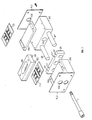
- the supporting mechanical part shown in Fig. 1, supports two dielectric substrates whereupon electrical circuits are constructed and separately connected to the gate and drain of the FET under test. It can be adapted to the geometrical sizes of the component case and allows the FET to be submitted to thermal tests avoiding too great stresses due to expansion.
- the intermediate block is made every time with width and height suited to match the dimensions of the case of the FET under test. Namely the width will be more or less equal to the case width and the height will be such as to allow FET terminals to easily rely on the electrical circuit lines.
- the FET can be fixed on the intermediate block by screws screwed into holes FT′ and FT ⁇ , while holes FP′ and FP ⁇ allow a pressing element PR, described hereinafter, to be fastened.
- This intermediate block is also designed to guarantee the electrical contact to FET source and the thermal contact to the whole component; - two small plugs SP′ and SP ⁇ to align the two supporting blocks and the intermediate block when they are blocked by screw V, passing through SU2 and IN and screwed into threaded hole FF of SU1; - two plates P01 and P02, screwed to supporting blocks SU1 and SU2, support the already-mentioned dielectric substrates CI1 and CI2.
- Plates P01 and P02 are meant to adapt thermal expansions of supporting blocks SU1 and SU2 to thermal expansions of dielectric substrates CI1 and CI2, in order to avoid excessive mechanical stresses during heating cycles occurring while measuring the FET under test.
- the material P01 and P02 are made of is then to present a thermal expansion coefficient which is intermediate between that of the plates and that of the dielectric substrates: e.g.
- P01 and P02 can be made of an iron-nickel-cobalt alloy, the so-called kovar; - the already-mentioned pressing element PR is made of the same material as plates P01 and P02 and supplied with two insulating bars SE1 and SE2, adapted to press FET gate and drain terminals onto substrates CI1 and CI2 to ensure their electrical contact without requiring soldering.
- each one of the substrates CI1 and CI2 can be seen in Fig. 2.
- dielectric substrate made of quartz, alumina, beryllium oxide or the like
- line PC is made of conductive material, e.g. of gold, and is equipped on one end with a pad for the connection to the power-supply connector.
- the gate or drain of the FET under test is placed in contact.
- Two resistive lines RP′ and RP ⁇ are placed in contact with both edges of line PC.
- Said lines can be made of suitable resistive substances, e.g. TaN or others.
- conductive lines PL′ and PL ⁇ are also placed in contact with the ends of the branches perpendicular to the resistive lines RP′ and RP ⁇ .
- Lines PL′ and PL ⁇ are in turn connected to capacitor terminals (not shown in the Figure), which are grounded through plates P01 and P02 (Fig. 1).
- the lateral ends of resistive lines RP′ and RP ⁇ result grounded in ac current and insulated in dc current. This circuit can be constructed with the thin film technique.
- the resistive lines parallel to the conductive lines are equivalent to sets of resistance A′ and A ⁇ , the perpendicular lines to sets of resistances B′ and B ⁇ , in addition there are sets of grounded capacitors C′ and C ⁇ .
- Each set of capacitors consist of at least a high capacitance capacitor and one of low capacity, so as to reduce parasitic reactance both at low and high frequencies.
- the equivalent high-frequency resistances seen from FET gate or drain towards the ground can thus be conveniently set to about 50 ohm. This value has been obtained by two resistive parallel branches, but it could also be obtained by three or more branches of less width.
Landscapes
- Engineering & Computer Science (AREA)
- Computer Hardware Design (AREA)
- Microelectronics & Electronic Packaging (AREA)
- Physics & Mathematics (AREA)
- General Physics & Mathematics (AREA)
- Testing Of Individual Semiconductor Devices (AREA)
- Non-Reversible Transmitting Devices (AREA)
Applications Claiming Priority (2)
| Application Number | Priority Date | Filing Date | Title |
|---|---|---|---|
| IT67258/88A IT1219140B (it) | 1988-03-23 | 1988-03-23 | Dispositivo per la misura delle caratteristiche statiche di componenti attivi a tre terminali per microonde |
| IT6725888 | 1988-03-23 |
Publications (3)
| Publication Number | Publication Date |
|---|---|
| EP0334273A2 true EP0334273A2 (de) | 1989-09-27 |
| EP0334273A3 EP0334273A3 (en) | 1990-07-25 |
| EP0334273B1 EP0334273B1 (de) | 1993-09-29 |
Family
ID=11300918
Family Applications (1)
| Application Number | Title | Priority Date | Filing Date |
|---|---|---|---|
| EP89104997A Expired - Lifetime EP0334273B1 (de) | 1988-03-23 | 1989-03-21 | Befestigungsanordnung für das Messen der statischen Charakteristika von aktiven Mikrowellenkomponenten mit 3 Anschlüssen |
Country Status (6)
| Country | Link |
|---|---|
| US (1) | US4912402A (de) |
| EP (1) | EP0334273B1 (de) |
| JP (1) | JPH0677045B2 (de) |
| CA (1) | CA1305219C (de) |
| DE (2) | DE68909456T2 (de) |
| IT (1) | IT1219140B (de) |
Families Citing this family (5)
| Publication number | Priority date | Publication date | Assignee | Title |
|---|---|---|---|---|
| US5477137A (en) * | 1992-10-02 | 1995-12-19 | Motorola, Inc. | Probeable substrate substitute for a calibration standard and test fixture |
| US5420506A (en) * | 1993-06-18 | 1995-05-30 | Industrial Technology Research Institute | Apparatus and method for testing packaged integrated circuits |
| USRE45667E1 (en) * | 2000-06-13 | 2015-09-08 | Christos Tsironis | Adaptable pre-matched tuner system and method |
| US11029351B1 (en) * | 2018-08-20 | 2021-06-08 | Christos Tsironis | Transforming load pull test fixture for wave measurements |
| RU2770299C1 (ru) * | 2021-03-19 | 2022-04-15 | Федеральное государственное бюджетное образовательное учреждение высшего образования "Пензенский государственный университет" | Способ определения параметров трехэлементного резонансного двухполюсника и измерительная цепь для его осуществления |
Family Cites Families (7)
| Publication number | Priority date | Publication date | Assignee | Title |
|---|---|---|---|---|
| IT1125389B (it) * | 1979-06-28 | 1986-05-14 | Cise Spa | Struttura periodica di trasmissione di segnali ad onda lenta per elementi circuitali monolitici miniaturizzati operanti a frequenza di microonde |
| US4535307A (en) * | 1982-06-30 | 1985-08-13 | Raytheon Company | Microwave circuit device package |
| US4538124A (en) * | 1984-02-10 | 1985-08-27 | Rca Corporation | Planar microwave circuit component mounting system |
| US4733209A (en) * | 1986-06-27 | 1988-03-22 | Augat Inc. | Ceramic Scrambler module |
| JPS6313502A (ja) * | 1986-07-04 | 1988-01-20 | Yuniden Kk | マイクロ波方向性結合器 |
| US4764723A (en) * | 1986-11-10 | 1988-08-16 | Cascade Microtech, Inc. | Wafer probe |
| FR2608772B1 (fr) * | 1986-12-23 | 1989-03-31 | Thomson Semiconducteurs | Dispositif de mesure des caracteristiques d'un composant hyperfrequence |
-
1988
- 1988-03-23 IT IT67258/88A patent/IT1219140B/it active
-
1989
- 1989-02-27 US US07/316,409 patent/US4912402A/en not_active Expired - Fee Related
- 1989-03-08 JP JP1053979A patent/JPH0677045B2/ja not_active Expired - Lifetime
- 1989-03-10 CA CA000593370A patent/CA1305219C/en not_active Expired - Lifetime
- 1989-03-21 DE DE89104997T patent/DE68909456T2/de not_active Expired - Fee Related
- 1989-03-21 DE DE198989104997T patent/DE334273T1/de active Pending
- 1989-03-21 EP EP89104997A patent/EP0334273B1/de not_active Expired - Lifetime
Also Published As
| Publication number | Publication date |
|---|---|
| JPH01276077A (ja) | 1989-11-06 |
| EP0334273A3 (en) | 1990-07-25 |
| DE334273T1 (de) | 1990-12-20 |
| CA1305219C (en) | 1992-07-14 |
| IT1219140B (it) | 1990-05-03 |
| DE68909456D1 (de) | 1993-11-04 |
| DE68909456T2 (de) | 1994-03-03 |
| JPH0677045B2 (ja) | 1994-09-28 |
| US4912402A (en) | 1990-03-27 |
| IT8867258A0 (it) | 1988-03-23 |
| EP0334273B1 (de) | 1993-09-29 |
Similar Documents
| Publication | Publication Date | Title |
|---|---|---|
| US3652941A (en) | Double balanced microwave mixer using balanced microstrip baluns | |
| Beilenhoff et al. | Open and short circuits in coplanar MMIC's | |
| RU2137264C1 (ru) | Устройство деления и суммирования радиочастотной мощности | |
| EP0680141B1 (de) | Verbesserungen der Frequenzcharakteristik einer Halbleiteranordnung in einem Mikrowellenfrequenzband | |
| JPS6157715B2 (de) | ||
| JPH0514069A (ja) | 高出力電界効果トランジスタ増幅器 | |
| EP0334273B1 (de) | Befestigungsanordnung für das Messen der statischen Charakteristika von aktiven Mikrowellenkomponenten mit 3 Anschlüssen | |
| US5598131A (en) | AC coupled termination | |
| EP0117434A1 (de) | Hybrides Mikrowellenteilsystem | |
| US4800343A (en) | DC cutting circuit | |
| US3470483A (en) | Miniature microwave broadband detector devices | |
| US7196909B2 (en) | AC coupling circuit having a large capacitance and a good frequency response | |
| US6181147B1 (en) | Device evaluation circuit | |
| JPH0427874A (ja) | 高周波素子測定用プローブヘッド | |
| US4484163A (en) | Arrangement for biasing high-frequency active components | |
| JPH03218102A (ja) | インターデジタルフィルタ | |
| JP3448833B2 (ja) | 伝送線路及び半導体装置 | |
| JP2701825B2 (ja) | 高周波特性の測定方法 | |
| US4118672A (en) | Attenuation equalizer having constant resistance | |
| JPS5811746B2 (ja) | 超高周波トランジスタ増幅器 | |
| JPH0262064A (ja) | セラミックパッケージ | |
| Hallford | Low noise microstrip mixer on a plastic substrate | |
| Temple et al. | Techniques for improving the stability and amplifier performance of X-band GaAs power FETs | |
| US4713730A (en) | Microwave plug-in signal amplifying module solderment apparatus | |
| JPS5846565Y2 (ja) | マイクロ波用半導体装置 |
Legal Events
| Date | Code | Title | Description |
|---|---|---|---|
| PUAI | Public reference made under article 153(3) epc to a published international application that has entered the european phase |
Free format text: ORIGINAL CODE: 0009012 |
|
| AK | Designated contracting states |
Kind code of ref document: A2 Designated state(s): DE FR GB NL SE |
|
| PUAL | Search report despatched |
Free format text: ORIGINAL CODE: 0009013 |
|
| RHK1 | Main classification (correction) |
Ipc: G01R 31/26 |
|
| AK | Designated contracting states |
Kind code of ref document: A3 Designated state(s): DE FR GB NL SE |
|
| 17P | Request for examination filed |
Effective date: 19900928 |
|
| EL | Fr: translation of claims filed | ||
| TCNL | Nl: translation of patent claims filed | ||
| DET | De: translation of patent claims | ||
| 17Q | First examination report despatched |
Effective date: 19920706 |
|
| GRAA | (expected) grant |
Free format text: ORIGINAL CODE: 0009210 |
|
| AK | Designated contracting states |
Kind code of ref document: B1 Designated state(s): DE FR GB NL SE |
|
| REF | Corresponds to: |
Ref document number: 68909456 Country of ref document: DE Date of ref document: 19931104 |
|
| ET | Fr: translation filed | ||
| PLBE | No opposition filed within time limit |
Free format text: ORIGINAL CODE: 0009261 |
|
| STAA | Information on the status of an ep patent application or granted ep patent |
Free format text: STATUS: NO OPPOSITION FILED WITHIN TIME LIMIT |
|
| 26N | No opposition filed | ||
| EAL | Se: european patent in force in sweden |
Ref document number: 89104997.5 |
|
| PGFP | Annual fee paid to national office [announced via postgrant information from national office to epo] |
Ref country code: SE Payment date: 19950228 Year of fee payment: 7 |
|
| PGFP | Annual fee paid to national office [announced via postgrant information from national office to epo] |
Ref country code: GB Payment date: 19950313 Year of fee payment: 7 |
|
| PGFP | Annual fee paid to national office [announced via postgrant information from national office to epo] |
Ref country code: DE Payment date: 19950329 Year of fee payment: 7 |
|
| PGFP | Annual fee paid to national office [announced via postgrant information from national office to epo] |
Ref country code: NL Payment date: 19950331 Year of fee payment: 7 Ref country code: FR Payment date: 19950331 Year of fee payment: 7 |
|
| PG25 | Lapsed in a contracting state [announced via postgrant information from national office to epo] |
Ref country code: GB Effective date: 19960321 |
|
| PG25 | Lapsed in a contracting state [announced via postgrant information from national office to epo] |
Ref country code: SE Effective date: 19960322 |
|
| PG25 | Lapsed in a contracting state [announced via postgrant information from national office to epo] |
Ref country code: NL Effective date: 19961001 |
|
| GBPC | Gb: european patent ceased through non-payment of renewal fee |
Effective date: 19960321 |
|
| PG25 | Lapsed in a contracting state [announced via postgrant information from national office to epo] |
Ref country code: FR Effective date: 19961129 |
|
| NLV4 | Nl: lapsed or anulled due to non-payment of the annual fee |
Effective date: 19961001 |
|
| PG25 | Lapsed in a contracting state [announced via postgrant information from national office to epo] |
Ref country code: DE Effective date: 19961203 |
|
| EUG | Se: european patent has lapsed |
Ref document number: 89104997.5 |
|
| REG | Reference to a national code |
Ref country code: FR Ref legal event code: ST |