EP0334637A2 - Dispositif à semi-conducteur - Google Patents
Dispositif à semi-conducteur Download PDFInfo
- Publication number
- EP0334637A2 EP0334637A2 EP89302854A EP89302854A EP0334637A2 EP 0334637 A2 EP0334637 A2 EP 0334637A2 EP 89302854 A EP89302854 A EP 89302854A EP 89302854 A EP89302854 A EP 89302854A EP 0334637 A2 EP0334637 A2 EP 0334637A2
- Authority
- EP
- European Patent Office
- Prior art keywords
- layer
- carrier density
- type
- gaas
- semiconductor
- Prior art date
- Legal status (The legal status is an assumption and is not a legal conclusion. Google has not performed a legal analysis and makes no representation as to the accuracy of the status listed.)
- Withdrawn
Links
Images


Classifications
-
- H—ELECTRICITY
- H10—SEMICONDUCTOR DEVICES; ELECTRIC SOLID-STATE DEVICES NOT OTHERWISE PROVIDED FOR
- H10H—INORGANIC LIGHT-EMITTING SEMICONDUCTOR DEVICES HAVING POTENTIAL BARRIERS
- H10H20/00—Individual inorganic light-emitting semiconductor devices having potential barriers, e.g. light-emitting diodes [LED]
- H10H20/80—Constructional details
- H10H20/81—Bodies
- H10H20/822—Materials of the light-emitting regions
- H10H20/824—Materials of the light-emitting regions comprising only Group III-V materials, e.g. GaP
-
- H—ELECTRICITY
- H01—ELECTRIC ELEMENTS
- H01S—DEVICES USING THE PROCESS OF LIGHT AMPLIFICATION BY STIMULATED EMISSION OF RADIATION [LASER] TO AMPLIFY OR GENERATE LIGHT; DEVICES USING STIMULATED EMISSION OF ELECTROMAGNETIC RADIATION IN WAVE RANGES OTHER THAN OPTICAL
- H01S5/00—Semiconductor lasers
- H01S5/04—Processes or apparatus for excitation, e.g. pumping, e.g. by electron beams
- H01S5/042—Electrical excitation ; Circuits therefor
- H01S5/0421—Electrical excitation ; Circuits therefor characterised by the semiconducting contacting layers
-
- H—ELECTRICITY
- H10—SEMICONDUCTOR DEVICES; ELECTRIC SOLID-STATE DEVICES NOT OTHERWISE PROVIDED FOR
- H10D—INORGANIC ELECTRIC SEMICONDUCTOR DEVICES
- H10D62/00—Semiconductor bodies, or regions thereof, of devices having potential barriers
- H10D62/80—Semiconductor bodies, or regions thereof, of devices having potential barriers characterised by the materials
- H10D62/85—Semiconductor bodies, or regions thereof, of devices having potential barriers characterised by the materials being Group III-V materials, e.g. GaAs
-
- H—ELECTRICITY
- H10—SEMICONDUCTOR DEVICES; ELECTRIC SOLID-STATE DEVICES NOT OTHERWISE PROVIDED FOR
- H10D—INORGANIC ELECTRIC SEMICONDUCTOR DEVICES
- H10D64/00—Electrodes of devices having potential barriers
- H10D64/60—Electrodes characterised by their materials
- H10D64/62—Electrodes ohmically coupled to a semiconductor
-
- H—ELECTRICITY
- H10—SEMICONDUCTOR DEVICES; ELECTRIC SOLID-STATE DEVICES NOT OTHERWISE PROVIDED FOR
- H10H—INORGANIC LIGHT-EMITTING SEMICONDUCTOR DEVICES HAVING POTENTIAL BARRIERS
- H10H20/00—Individual inorganic light-emitting semiconductor devices having potential barriers, e.g. light-emitting diodes [LED]
- H10H20/01—Manufacture or treatment
- H10H20/011—Manufacture or treatment of bodies, e.g. forming semiconductor layers
- H10H20/013—Manufacture or treatment of bodies, e.g. forming semiconductor layers having light-emitting regions comprising only Group III-V materials
-
- H—ELECTRICITY
- H01—ELECTRIC ELEMENTS
- H01S—DEVICES USING THE PROCESS OF LIGHT AMPLIFICATION BY STIMULATED EMISSION OF RADIATION [LASER] TO AMPLIFY OR GENERATE LIGHT; DEVICES USING STIMULATED EMISSION OF ELECTROMAGNETIC RADIATION IN WAVE RANGES OTHER THAN OPTICAL
- H01S5/00—Semiconductor lasers
- H01S5/20—Structure or shape of the semiconductor body to guide the optical wave ; Confining structures perpendicular to the optical axis, e.g. index or gain guiding, stripe geometry, broad area lasers, gain tailoring, transverse or lateral reflectors, special cladding structures, MQW barrier reflection layers
- H01S5/22—Structure or shape of the semiconductor body to guide the optical wave ; Confining structures perpendicular to the optical axis, e.g. index or gain guiding, stripe geometry, broad area lasers, gain tailoring, transverse or lateral reflectors, special cladding structures, MQW barrier reflection layers having a ridge or stripe structure
- H01S5/223—Buried stripe structure
- H01S5/2231—Buried stripe structure with inner confining structure only between the active layer and the upper electrode
-
- H—ELECTRICITY
- H01—ELECTRIC ELEMENTS
- H01S—DEVICES USING THE PROCESS OF LIGHT AMPLIFICATION BY STIMULATED EMISSION OF RADIATION [LASER] TO AMPLIFY OR GENERATE LIGHT; DEVICES USING STIMULATED EMISSION OF ELECTROMAGNETIC RADIATION IN WAVE RANGES OTHER THAN OPTICAL
- H01S5/00—Semiconductor lasers
- H01S5/30—Structure or shape of the active region; Materials used for the active region
- H01S5/32—Structure or shape of the active region; Materials used for the active region comprising PN junctions, e.g. hetero- or double- heterostructures
- H01S5/323—Structure or shape of the active region; Materials used for the active region comprising PN junctions, e.g. hetero- or double- heterostructures in AIIIBV compounds, e.g. AlGaAs-laser, InP-based laser
- H01S5/32308—Structure or shape of the active region; Materials used for the active region comprising PN junctions, e.g. hetero- or double- heterostructures in AIIIBV compounds, e.g. AlGaAs-laser, InP-based laser emitting light at a wavelength less than 900 nm
- H01S5/32325—Structure or shape of the active region; Materials used for the active region comprising PN junctions, e.g. hetero- or double- heterostructures in AIIIBV compounds, e.g. AlGaAs-laser, InP-based laser emitting light at a wavelength less than 900 nm red laser based on InGaP
Definitions
- the present invention relates to a semiconductor device and, more particularly, to a semiconductor device in which an electric current is passed between a GaAs semiconductor layer and an InGaAlP semiconductor layer both having the same conductivity type.
- InGaAlP materials now receive widespread attention as materials for light emitting devices in the short wavelength range, these materials having the largest energy gap among alloys of group III-V compound semiconductors, except for nitrides.
- those compositions capable of lattice matching with GaAs can offer satisfactory epitaxial growth, with fewer crystal defects, by the metal organic chemical vapor deposition method (hereinafter abbreviated as MOCVD method).
- One method for avoiding such an adverse effect is to dispose, between the GaAs layer and the InGaAlP layer, an InGaAlP layer having a lower Al composition ratio and an intermediate energy gap between those two layers, for the purpose of effecting the ohmic injection of electric current (as disclosed in Japanese Patent Laid-Open No. 62-200784 (1987), for example).
- the provision of such an InGaAlP intermediate energy gap layer does not necessarily offer an ohmic characteristic.
- the voltage drop at the interface can give rise to the problem of increasing the operating voltage of the device.
- the resulting overheating creates high temperatures that impair the oscillation characteristics.
- a semiconductor device that achieves good ohmic contact between semiconductor layers, a low operating voltage and a satisfactory thermal characteristic.
- An electric current is caused to pass between an InGaAlP layer and a GaAs layer of the semiconductor device, both layers being of the same conductivity type, by providing in at least a part of the InGaAlP layer adjoining the GaAs layer, a higher carrier density region with the carrier density equal to or more than 5 x 10 17 cm ⁇ 3 and a thickness in a range of 400 ⁇ to 800 ⁇ .
- FIG. 1 is a conceptual view showing a first embodiment of the present invention.
- a semiconductor device 100 has an In l-x-y Ga y AL x P (0 ⁇ x,y ⁇ 1) layer 101, a higher carrier density region 102 in the In l-x-y Ga y Al x P layer 101, and a GaAs layer 103.
- the layers are of the same conductivity type and are illustrated as being p-type. It is important, particularly in light emitting devices or the like, that In l-x-y Ga y Al x P layer 101 is capable of lattice matching with GaAs layer 103, to assure the epitaxial layer grown on the GaAs layer of possibly perfect crystallinity.
- Fig. 2 shows the magnitude of voltage drop across the interface between GaAs layer 103 and the higher carrier density region 102 with respect to the carrier density p, with an injection current density 1 ka/cm2 applied to the device.
- FIG. 3 shows the voltage drop between GaAs layer 102 and an InGaAlP layer 101 with respect to the thickness d of higher carrier density region 102, with an injection current density of 1 kA/cm2 applied to the device and the carrier density of the higher carrier density region equal to 1 x 1018 cm ⁇ 3.
- d ⁇ 400 ⁇ the voltage increases drastically.
- d ⁇ 400 ⁇ the voltage drop gradually increased due to an increase in the series resistance with the increasing layer thickness.
- the current-voltage characteristic between GaAs layer 103 and InGaAlP layer 101 is largely affected by the carrier density p and the thickness d of higher carrier density region 102 formed in InGaAlP layer 101 adjacent the interface with GaAs layer 103, the carrier density p and the thickness d being required to fall in ranges of p ⁇ 5 x 1017 cm ⁇ 3 and d ⁇ 400 ⁇ , respectively.
- the carrier density p since the range of p > 3 x 1019 cm ⁇ 3 will cause the above-described problem, p is preferably maintained within a range of 5 x 1017 cm ⁇ 3 ⁇ p ⁇ 3 x 1019 cm ⁇ 3.
- Fig. 4 shows a semiconductor light emitting device according to a second embodiment of the present invention, and is a sectional view showing the schematic structure of a semiconductor laser in which a GaAs layer and an InGaAlP layer serve as an ohmic contact layer and a clad layer, respectively.
- the device comprises an n-GaAs substrate 401.
- a double heterojunction comprising a n-In l-w-z Ga z Al w P (0 ⁇ w,z ⁇ 1) clad layer 402, an In l-s-t Ga t Al s P (0 ⁇ s,t ⁇ 1) active layer 403, and a p-In l- u-v Ga v Al u P (0 ⁇ u,v ⁇ 1) clad layer 404, the junction serving as a light emitting active part.
- a p-GaAs ohmic contact layer 407 is formed over the portion of p-InGaP cap layer 405 where the overlying n-GaAs current restricting layer 406 has been removed, and also over the remaining portions of n-GaAs current restricting layer 406. Furthermore, an electrode 408 is formed on the bottom of substrate 401 and an electrode 409 is formed on the top of p-GaAs layer 407. Composition ratios of In, Ga and Al are set so that the respective layers constituting the double heterojunction and p-InGaP cap layer 405 have their lattice constants substantially equal to that of the substrate, and clad layers 402,404 have their band cap energies larger than that of active layer 403.
- the strip of n-GaAs current restricting layer 406 selectively removed has a width of 7 ⁇ m and a cavity length of 300 ⁇ m.
- the semiconductor laser exhibited an oscillation threshold current of 70 mA in the pulse operation mode and 72 mA in the continuous operation mode.
- the change in oscillation threshold current caused by generated heat is very small as compared with the value in the pulse operation mode.
- the operating voltage exhibited a very large value of 3.0 volt.
- the generated heat in the continuous operation mode was increased and the oscillation threshold current reached as high as 77 mA.
- the maximum continuous oscillation temperature was as low as 60°C. This may likely be attributable to the fact that the excessive voltage drop occurs across the heterojunction interfaces of p-GaAs/p-InGaP/p-InGaAlP.
- the operating voltage exhibited a very large value of 3.0 volt.
- the generated heat in the continuous operation mode increased and the oscillation threshold current reached as high as 77 mA.
- the maximum continuous oscillation temperature was as low as 60°C.
- the maximum continuous oscillation temperature experienced was as low as 30°C due to increases in both the thermal resistance and threshold current resulting from the current being more widely spread, as well as an increase in the generated heat resulting from the increased series resistance.
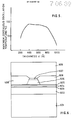
- Fig. 5 shows the dependence of the maximum continuous oscillation temperature on a thickness d of p-InGaP cap layer 405.
- the maximum continuous oscillation temperature exhibited a high value of more than 80°C, the temperatures experienced outside that thickness range being substantially lower.
- the maximum continuous oscillation temperature became more than 85°C, so that a very satisfactory thermal characteristic was observed.
- the achievement of continuous oscillation at these temperatures is a substantial improvement over prior art devices
- Fig. 6 shows a semiconductor light emitting device according to a third embodiment of the present invention, and is a sectional view showing the schematic structure of a semiconductor laser in which a GaAs layer and an InGaAlP layer serve as an ohmic contact layer and clad layer, respectively.
- the device comprises an n-GaAs substrate 601.
- a double heterojunction comprising an n-In l-w-z Ga z Al w P (0 ⁇ w, z ⁇ 1) clad layer 602, an In l-s-t Ga t Al s P (0 ⁇ s,t ⁇ 1) active layer 603, a p-In l-r-s Ga s Al r P (0 ⁇ r,s ⁇ 1) first clad layer 604, a p-In l-p-q Ga q Al p P (0 ⁇ p,q ⁇ 1) etching stopper layer 605 and a p-In l-u-v Ga v Al u P (0 ⁇ u,v ⁇ 1) second clad layer 606 being in strip form and convex in section, the junction serving as a light emitting active part.
- p-InGaP In l-x-y Ga y Al x P; 0 ⁇ x,y ⁇ 1
- a p-GaAs ohmic contact layer 609 is formed over p-InGaP cap layer 607 and n-GaAs current restricting layers 608. Furthermore, an electrode 610 is formed on the bottom of substrate 601, and an electrode 611 is formed on the top of p-GaAs layer 609. Composition ratios of In, Ga and Al are set so that the respective layers constituting the double heterojunction and the p-InGaP cap layer 607 have their lattice constants substantially equal to that of the substrate, and the clad layers 602, 604, 606 respectively have band gap energies larger than that of active layer 603.
- the strip width and the cavity length were selected to be 5 ⁇ m and 300 ⁇ m, respectively.
- the maximum continuous oscillation temperature of the semiconductor laser illustrated in Fig. 6 is dependent on both the carrier density and the thickness of p-InGaP cap layer 607. This dependency was found to be substantially identical to that of the device having the structure of the second embodiment shown in Fig. 4. With respect to the device having the structure of the third embodiment, when forming p-InGaAlP clad layer 606 in strip form and convexed, it is necessary to selectively remove p-InGaP cap layer 607 except for areas corresponding to the convex portions of layer 606.
- the etching rates of p-InGaAlP clad layer 606 and p-InGaP cap layer 607 tend to be partially increased in the vicinity of the strip projecting portions. For this reason, in order to achieve flat and satisfactory etching, it is desirable to minimize the thickness of p-InGaP cap layer 607 and hence make as short as possible the etching time necessary for removing p-InGaP cap layer 607.
- the thickness of p-InGaP cap layer 607 allowing such flat and satisfactory etching was found to be less than 600 ⁇ .
- the cap layer may generally be formed of InGaAlP as well.
- the cap layer is selected to have an energy gap smaller than that of the clad layer, so that the difference in energy gap between the cap layer and the GaAs layer is reduced, thereby making it easier to obtain an ohmic characteristic.
- the present invention is also applicable to any semiconductor devices, such as light emitting diodes and other electronic elements, which have a contact interface between an InGaAlP layer and a GaAs layer both having the same conductivity type, and having a function of passing an electric current through that interface.
- the present invention can be practiced in other various modified forms without departing from the scope of the present invention.
Landscapes
- Physics & Mathematics (AREA)
- Condensed Matter Physics & Semiconductors (AREA)
- General Physics & Mathematics (AREA)
- Electromagnetism (AREA)
- Optics & Photonics (AREA)
- Semiconductor Lasers (AREA)
- Led Devices (AREA)
- Junction Field-Effect Transistors (AREA)
Applications Claiming Priority (2)
| Application Number | Priority Date | Filing Date | Title |
|---|---|---|---|
| JP63069640A JP2685209B2 (ja) | 1988-03-25 | 1988-03-25 | 半導体装置及び半導体発光装置 |
| JP69640/88 | 1988-03-25 |
Publications (2)
| Publication Number | Publication Date |
|---|---|
| EP0334637A2 true EP0334637A2 (fr) | 1989-09-27 |
| EP0334637A3 EP0334637A3 (fr) | 1991-09-25 |
Family
ID=13408662
Family Applications (1)
| Application Number | Title | Priority Date | Filing Date |
|---|---|---|---|
| EP19890302854 Withdrawn EP0334637A3 (fr) | 1988-03-25 | 1989-03-22 | Dispositif à semi-conducteur |
Country Status (3)
| Country | Link |
|---|---|
| US (1) | US5138404A (fr) |
| EP (1) | EP0334637A3 (fr) |
| JP (1) | JP2685209B2 (fr) |
Cited By (12)
| Publication number | Priority date | Publication date | Assignee | Title |
|---|---|---|---|---|
| EP0427003A1 (fr) * | 1989-10-16 | 1991-05-15 | Kabushiki Kaisha Toshiba | Elément semi-conducteur émetteur de lumière et méthode de fabrication |
| EP0434233A1 (fr) * | 1989-12-18 | 1991-06-26 | Hewlett-Packard Company | Diode électroluminescente comportant une couche fenêtre électriquement conductrice |
| EP0449553A3 (en) * | 1990-03-27 | 1992-01-22 | Sony Corporation | Semiconductor lasers |
| EP0456429A3 (en) * | 1990-05-07 | 1992-03-11 | Kabushiki Kaisha Toshiba | Semiconductor laser device |
| EP0462816A3 (en) * | 1990-06-21 | 1992-04-15 | Mitsubishi Denki Kabushiki Kaisha | Semiconductor laser producing visible light |
| FR2675312A1 (fr) * | 1991-04-09 | 1992-10-16 | Mitsubishi Electric Corp | Procede de fabrication d'une diode laser en gaas emettant de la lumiere visible. |
| EP0574947A1 (fr) * | 1992-06-19 | 1993-12-22 | Sony Corporation | Dispositif d'émission de la lumière |
| US5278857A (en) * | 1989-10-16 | 1994-01-11 | Kabushiki Kaisha Toshiba | Indium gallium aluminum phosphide silicon doped to prevent zinc disordering |
| US6037603A (en) * | 1996-05-01 | 2000-03-14 | Epitaxial Products International Limited | Opto-electronic device with transparent high lateral conductivity current spreading layer |
| US6246078B1 (en) | 1997-01-29 | 2001-06-12 | Sharp Kabushiki Kaisha | Semiconductor light emitting element |
| DE19808446C2 (de) * | 1997-02-28 | 2003-03-13 | Sharp Kk | Halbleiter-Lichtemissionselement mit Stromdiffusionsschicht und Verfahren zum Herstellen desselben |
| US6577658B1 (en) | 1999-09-20 | 2003-06-10 | E20 Corporation, Inc. | Method and apparatus for planar index guided vertical cavity surface emitting lasers |
Families Citing this family (7)
| Publication number | Priority date | Publication date | Assignee | Title |
|---|---|---|---|---|
| JP3095545B2 (ja) * | 1992-09-29 | 2000-10-03 | 株式会社東芝 | 面発光型半導体発光装置およびその製造方法 |
| JP3217490B2 (ja) * | 1992-09-29 | 2001-10-09 | 株式会社東芝 | 半導体発光装置 |
| JP3198016B2 (ja) * | 1994-08-25 | 2001-08-13 | シャープ株式会社 | 発光ダイオードアレイ及びその製造方法 |
| US6996150B1 (en) | 1994-09-14 | 2006-02-07 | Rohm Co., Ltd. | Semiconductor light emitting device and manufacturing method therefor |
| JP3233569B2 (ja) * | 1996-03-22 | 2001-11-26 | シャープ株式会社 | 半導体発光素子 |
| JP3797748B2 (ja) | 1997-05-30 | 2006-07-19 | シャープ株式会社 | 発光ダイオードアレイ |
| US20040227141A1 (en) * | 2003-01-30 | 2004-11-18 | Epistar Corporation | Light emitting device having a high resistivity cushion layer |
Family Cites Families (11)
| Publication number | Priority date | Publication date | Assignee | Title |
|---|---|---|---|---|
| US4661961A (en) * | 1983-06-20 | 1987-04-28 | American Telephone And Telegraph Company, At&T Bell Laboratories | Buried heterostructure devices with unique contact-facilitating layers |
| US4617724A (en) * | 1983-06-30 | 1986-10-21 | Fujitsu Limited | Process for fabricating heterojunction bipolar transistor with low base resistance |
| JPS6055678A (ja) * | 1983-09-06 | 1985-03-30 | Nec Corp | 発光ダイオ−ド |
| JPH0647420B2 (ja) * | 1985-07-15 | 1994-06-22 | 松下電器産業株式会社 | 給紙カセツト |
| US4837775A (en) * | 1985-10-21 | 1989-06-06 | General Electric Company | Electro-optic device having a laterally varying region |
| JPH0671006B2 (ja) * | 1985-12-16 | 1994-09-07 | 日本電気株式会社 | バイポ−ラトランジスタ |
| US4792958A (en) * | 1986-02-28 | 1988-12-20 | Kabushiki Kaisha Toshiba | Semiconductor laser with mesa stripe waveguide structure |
| JPH0732285B2 (ja) * | 1986-02-28 | 1995-04-10 | 株式会社東芝 | 半導体レ−ザ装置 |
| EP0259026B1 (fr) * | 1986-08-08 | 1994-04-27 | Kabushiki Kaisha Toshiba | Laser à semi-conducteur à double-hétérostructure avec un guide d'ondes à ruban mesa |
| JP2564813B2 (ja) * | 1987-01-21 | 1996-12-18 | 日本電気株式会社 | A▲l▼GaInP半導体発光素子 |
| US5034957A (en) * | 1988-02-10 | 1991-07-23 | Kabushiki Kaisha Toshiba | Semiconductor laser device |
-
1988
- 1988-03-25 JP JP63069640A patent/JP2685209B2/ja not_active Expired - Lifetime
-
1989
- 1989-03-22 EP EP19890302854 patent/EP0334637A3/fr not_active Withdrawn
-
1991
- 1991-05-31 US US07/708,806 patent/US5138404A/en not_active Expired - Lifetime
Cited By (20)
| Publication number | Priority date | Publication date | Assignee | Title |
|---|---|---|---|---|
| US5278857A (en) * | 1989-10-16 | 1994-01-11 | Kabushiki Kaisha Toshiba | Indium gallium aluminum phosphide silicon doped to prevent zinc disordering |
| EP0427003A1 (fr) * | 1989-10-16 | 1991-05-15 | Kabushiki Kaisha Toshiba | Elément semi-conducteur émetteur de lumière et méthode de fabrication |
| EP0434233A1 (fr) * | 1989-12-18 | 1991-06-26 | Hewlett-Packard Company | Diode électroluminescente comportant une couche fenêtre électriquement conductrice |
| EP0449553A3 (en) * | 1990-03-27 | 1992-01-22 | Sony Corporation | Semiconductor lasers |
| EP0456429A3 (en) * | 1990-05-07 | 1992-03-11 | Kabushiki Kaisha Toshiba | Semiconductor laser device |
| US5202895A (en) * | 1990-05-07 | 1993-04-13 | Kabushiki Kaisha Toshiba | Semiconductor device having an active layer made of ingaalp material |
| EP0462816A3 (en) * | 1990-06-21 | 1992-04-15 | Mitsubishi Denki Kabushiki Kaisha | Semiconductor laser producing visible light |
| US5161167A (en) * | 1990-06-21 | 1992-11-03 | Mitsubishi Denki Kabushiki Kaisha | Semiconductor laser producing visible light |
| FR2675312A1 (fr) * | 1991-04-09 | 1992-10-16 | Mitsubishi Electric Corp | Procede de fabrication d'une diode laser en gaas emettant de la lumiere visible. |
| US5272109A (en) * | 1991-04-09 | 1993-12-21 | Mitsubishi Denki Kabushiki Kaisha | Method for fabricating visible light laser diode |
| EP0574947A1 (fr) * | 1992-06-19 | 1993-12-22 | Sony Corporation | Dispositif d'émission de la lumière |
| US5471067A (en) * | 1992-06-19 | 1995-11-28 | Sony Corporation | Semiconductor metal contacting structure and a light emitting device |
| US6037603A (en) * | 1996-05-01 | 2000-03-14 | Epitaxial Products International Limited | Opto-electronic device with transparent high lateral conductivity current spreading layer |
| US6246078B1 (en) | 1997-01-29 | 2001-06-12 | Sharp Kabushiki Kaisha | Semiconductor light emitting element |
| US6399409B2 (en) | 1997-01-29 | 2002-06-04 | Sharp Kabushiki Kaisha | Method for fabricating semiconductor light emitting element |
| DE19803006B4 (de) * | 1997-01-29 | 2007-03-15 | Sharp K.K. | Halbleiter-Lichtemissionselement |
| DE19808446C2 (de) * | 1997-02-28 | 2003-03-13 | Sharp Kk | Halbleiter-Lichtemissionselement mit Stromdiffusionsschicht und Verfahren zum Herstellen desselben |
| US6577658B1 (en) | 1999-09-20 | 2003-06-10 | E20 Corporation, Inc. | Method and apparatus for planar index guided vertical cavity surface emitting lasers |
| US6822993B2 (en) | 1999-09-20 | 2004-11-23 | Jds Uniphase Corporation | Index guided vertical cavity surface emitting lasers |
| US6852558B2 (en) | 1999-09-20 | 2005-02-08 | Jds Uniphase Corporation | Methods for forming index guided vertical cavity surface emitting lasers |
Also Published As
| Publication number | Publication date |
|---|---|
| US5138404A (en) | 1992-08-11 |
| EP0334637A3 (fr) | 1991-09-25 |
| JPH01243597A (ja) | 1989-09-28 |
| JP2685209B2 (ja) | 1997-12-03 |
Similar Documents
| Publication | Publication Date | Title |
|---|---|---|
| EP0334637A2 (fr) | Dispositif à semi-conducteur | |
| US5821555A (en) | Semicoductor device having a hetero interface with a lowered barrier | |
| USRE37177E1 (en) | Semiconductor laser | |
| EP1560276B1 (fr) | Dispositif émettant de lumière fabriqué de matériau III-nitrure ayant des champs de polarisation réduits | |
| US6995389B2 (en) | Heterostructures for III-nitride light emitting devices | |
| US6242761B1 (en) | Nitride compound semiconductor light emitting device | |
| US5585649A (en) | Compound semiconductor devices and methods of making compound semiconductor devices | |
| US7939833B2 (en) | Nitride semiconductor light emitting device | |
| EP1328050A2 (fr) | Structure laser à semiconducteur | |
| EP0373933B1 (fr) | Méthode de production d'un laser à semi-conducteur muni d'une structure non absorbante à miroir | |
| US7485902B2 (en) | Nitride-based semiconductor light-emitting device | |
| EP0554089B1 (fr) | Dispositif émetteur de lumière à semi-conducteur | |
| US6121638A (en) | Multi-layer structured nitride-based semiconductor devices | |
| EP0619613B1 (fr) | Transisitor bipolaire à hétérojonction | |
| KR19990068168A (ko) | 반도체 장치 및 그 제조 방법 | |
| US5786603A (en) | Multilayer structured semiconductor devices | |
| EP0834929B1 (fr) | Contact omique pour un semiconducteur composite n-GaN ou apparenté et sa méthode de fabrication | |
| US5539239A (en) | Semiconductor light emitting element with II-VI and III-V compounds | |
| US7791081B2 (en) | Radiation-emitting semiconductor chip | |
| KR100603681B1 (ko) | 반도체 레이저 소자 | |
| Susaki et al. | New structures of GaAlAs lateral-injection laser for low-threshold and single-mode operation | |
| US5898190A (en) | P-type electrode structure and a semiconductor light emitting element using the same structure | |
| US6861275B2 (en) | Method for producing group III nitride compound semiconductor device | |
| JP2790235B2 (ja) | 窒化ガリウム系化合物半導体のp型化方法 | |
| JP3221073B2 (ja) | 発光素子 |
Legal Events
| Date | Code | Title | Description |
|---|---|---|---|
| PUAI | Public reference made under article 153(3) epc to a published international application that has entered the european phase |
Free format text: ORIGINAL CODE: 0009012 |
|
| 17P | Request for examination filed |
Effective date: 19890412 |
|
| AK | Designated contracting states |
Kind code of ref document: A2 Designated state(s): DE FR GB |
|
| PUAL | Search report despatched |
Free format text: ORIGINAL CODE: 0009013 |
|
| AK | Designated contracting states |
Kind code of ref document: A3 Designated state(s): DE FR GB |
|
| 17Q | First examination report despatched |
Effective date: 19930421 |
|
| STAA | Information on the status of an ep patent application or granted ep patent |
Free format text: STATUS: THE APPLICATION IS DEEMED TO BE WITHDRAWN |
|
| 18D | Application deemed to be withdrawn |
Effective date: 19930902 |