EP0334954B1 - Reseau en couches - Google Patents
Reseau en couches Download PDFInfo
- Publication number
- EP0334954B1 EP0334954B1 EP89900410A EP89900410A EP0334954B1 EP 0334954 B1 EP0334954 B1 EP 0334954B1 EP 89900410 A EP89900410 A EP 89900410A EP 89900410 A EP89900410 A EP 89900410A EP 0334954 B1 EP0334954 B1 EP 0334954B1
- Authority
- EP
- European Patent Office
- Prior art keywords
- switch
- stage
- request
- terminal
- requests
- Prior art date
- Legal status (The legal status is an assumption and is not a legal conclusion. Google has not performed a legal analysis and makes no representation as to the accuracy of the status listed.)
- Expired - Lifetime
Links
Images


Classifications
-
- H—ELECTRICITY
- H04—ELECTRIC COMMUNICATION TECHNIQUE
- H04Q—SELECTING
- H04Q3/00—Selecting arrangements
- H04Q3/64—Distributing or queueing
- H04Q3/68—Grouping or interlacing selector groups or stages
-
- G—PHYSICS
- G06—COMPUTING OR CALCULATING; COUNTING
- G06F—ELECTRIC DIGITAL DATA PROCESSING
- G06F15/00—Digital computers in general; Data processing equipment in general
- G06F15/16—Combinations of two or more digital computers each having at least an arithmetic unit, a program unit and a register, e.g. for a simultaneous processing of several programs
- G06F15/163—Interprocessor communication
- G06F15/173—Interprocessor communication using an interconnection network, e.g. matrix, shuffle, pyramid, star, snowflake
- G06F15/17337—Direct connection machines, e.g. completely connected computers, point to point communication networks
-
- H—ELECTRICITY
- H04—ELECTRIC COMMUNICATION TECHNIQUE
- H04L—TRANSMISSION OF DIGITAL INFORMATION, e.g. TELEGRAPHIC COMMUNICATION
- H04L49/00—Packet switching elements
- H04L49/15—Interconnection of switching modules
- H04L49/1507—Distribute and route fabrics, e.g. sorting-routing or Batcher-Banyan
-
- H—ELECTRICITY
- H04—ELECTRIC COMMUNICATION TECHNIQUE
- H04L—TRANSMISSION OF DIGITAL INFORMATION, e.g. TELEGRAPHIC COMMUNICATION
- H04L49/00—Packet switching elements
- H04L49/10—Packet switching elements characterised by the switching fabric construction
- H04L49/101—Packet switching elements characterised by the switching fabric construction using crossbar or matrix
-
- H—ELECTRICITY
- H04—ELECTRIC COMMUNICATION TECHNIQUE
- H04L—TRANSMISSION OF DIGITAL INFORMATION, e.g. TELEGRAPHIC COMMUNICATION
- H04L49/00—Packet switching elements
- H04L49/20—Support for services
- H04L49/205—Quality of Service based
-
- H—ELECTRICITY
- H04—ELECTRIC COMMUNICATION TECHNIQUE
- H04L—TRANSMISSION OF DIGITAL INFORMATION, e.g. TELEGRAPHIC COMMUNICATION
- H04L49/00—Packet switching elements
- H04L49/25—Routing or path finding in a switch fabric
- H04L49/253—Routing or path finding in a switch fabric using establishment or release of connections between ports
- H04L49/254—Centralised controller, i.e. arbitration or scheduling
-
- H—ELECTRICITY
- H04—ELECTRIC COMMUNICATION TECHNIQUE
- H04L—TRANSMISSION OF DIGITAL INFORMATION, e.g. TELEGRAPHIC COMMUNICATION
- H04L49/00—Packet switching elements
- H04L49/40—Constructional details, e.g. power supply, mechanical construction or backplane
Definitions
- This invention relates to a network intercommunication system for providing communication between digital computers.
- the Layered network of the present invention spans the full range from very cheap, blocking networks to robust, complete routing networks. The system designer may select an appropriate member of the Layered class based on the system's requirements.
- Classical interconnection networks use distributed routing schemes to avoid the problems associated with centralized network control.
- the classical networks establish a connection by setting each switch by one of the bits in the "request.” The request is merely the number of the processor to which the connection should be made.
- N processor baseline network each of the log 2 N bits is used to set one of the log 2 N switches of size 2 by 2 in its path.
- N processor baseline network
- Blocking occurs when two requests arrive simultaneously at a switch and both need to use the same terminal.
- Layered networks may choose from more than one digit to route and therefore route connections that would normally be blocked.
- the crossbar switch (see p. 146 of Wu and Feng) can be routed in a fast non-blocking manner, but its cost rises rapidly with the number of processors to be connected.
- Wu and Feng show in their paper, "The Reverse Exchange Interconnection Network” (IEEE Trans Computer, September 1980), the functional relationship between many of the studied interconnection networks including: Baseline, Omega, Flip, Banyan, and others. They also identify the small subset of all possible permutations that those networks can perform.
- the topological transformations taught by Wu and Feng may be used in conjunction with the topology of the present invention and within the scope of the invention to provide alternate embodiments.
- Baseline networks have fast routing algorithms, but they are blocking. Wu and Feng also discuss the Benes network.
- the Benes network can be constructed by cascading two "baseline type” networks.
- the Benes network can implement all N factorial (N!) permutations.
- N factorial
- routing algorithms that allow all permutations, much less combinations, require centralized matrix manipulation.
- existing networks either are too costly (crossbar), lack an efficient routing algorithm (Cantor, Benes), or fail to implement all permutations and combinations (Baseline).
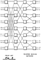
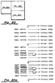
- the crossbar switch (Fig. 1) has been used in many prior interconnection systems for its high speed, repetitive construction, and full interconnect capability.
- a crossbar is basically a unidirectional device in which the outputs "listen" to the inputs. Each output can listen to any desired input without conflict.
- the crossbar's totally non-blocking property and distributed control serves as an ideal standard. However, the crossbar exhibits on the order of 0(N 2 ) cost growth and does not allow special broadcast operations where different listeners receive different values from the same input.
- the new class of Layered interconnection networks of the present disclosure satisfies these criteria and can provide all N interconnection patterns with 0(Nlog 3 N) cost growth.
- Layered Networks provide an alternative to highly-blocking classical networks equivalent to the Baseline network. Layered Networks support a much richer set of connections than classical networks.
- a subclass of Layered Networks, "binary, fully-Layered” networks, is shown to implement all connections possible with a crossbar using the distributed switch setting algorithm, but with much slower cost growth when scaled up to systems with more processors.
- the network of this disclosure (termed a Layered Network) comprises a class of multi-stage interconnection networks.
- the Layered network class spans the full range from very cheap, blocking networks to robust, completely routing networks. A system designer may select an appropriate member of the Layered Network class based on the particular system's requirements.
- a network interconnection system for connecting up to N responder means with up to N requestor means comprising
- the Layered Networks of the present disclosure are constructed with a multitude of switches with point- to-point connections between them.
- the network establishes connections from requestors to responders by relaying "requests" through the switches.
- Each switch has built-in control logic to route requests and responses.
- the switch setting is determined using the comparison of the request with the request's current location in the network.
- Each switch routes the requests using only the information contained in the requests and switch routes to provide distributed routing without a centralized controller.
- the switch setting is remembered to route the responses on the same paths as the associated requests, but in the reverse direction.
- Layered Networks are constructed such that a switch can route a signal to another switch that has the same switch-number except for a single b-ary digit in the next stage.
- a request contains a b-ary number identifying the desired response port.
- the switch compares the request with the switch-number. If the b-ary digit compared is the same, the request is routed straight, otherwise the request is routed to another switch that matches the digit in the request.
- the request should have reached the switch in the Iog b N t " stage whose switch number exactly matches the request.
- binary digits are employed.
- Classical interconnections networks use distributed routing schemes to avoid the problems associated with centralized network control.
- the classical networks establish a connection by setting each switch by one of the bits in the "request.” The request is merely the number of the processor to which the connection should be made.
- N processor Baseline network With an N processor Baseline network, each of log 2 N bits is used to set one of the log 2 N switches of size 2 by 2 in its path.
- Layered Networks may choose from more than one connection and can route requests and responses that are blocked by the classical, baseline-equivalent networks.
- N the number of processors connected to the network
- b- the base of logarithms and number representation
- p--the number of "planes" of connections in the network The planes in a Layered Network provide additional paths that reduce contention in switch setting.
- the Layered Networks are constructed such that a switch can route a signal (request or response data) to other switches in the next stage that has the same switch-number except for a single b-ary (base b) digit.
- the switch setting algorithm requires information regarding only those connections that use the switch. Each switch is set independently, without information exchange between switches in the same stage which allows distributed switch setting.
- the switch compares the request which is a b-ary number identifying the desired response port with the switch-number. If the b-ary digits compared are the same, the request is routed straight, otherwise the request is routed to another switch that matches the b-ary digit in the request. At the end of the network, the request should have reached the switch in the Iog b N t " stage whose switch number exactly matches the request.
- the Hamming distance between two numbers is the quantity of bits different between the numbers. Each bit is compared with a bit of the other number of equal significance and the differing bits are counted.
- the Hamming distance for a request is calculated by comparing the number that identifies the desired response port (referred to as the request) with the switch-number which identifies the switch it occupies.
- the request When the request's Hamming distance equals zero, the request equals the switch-number.
- the last stage switches are connected to response ports whose input-numbers match the switch-numbers. If a request reaches a last stage switch, and has Hamming distance zero, it has successfully routed the desired connection.
- the address with the largest hamming distance is eliminated from the file and the process is repeated using the remaining Search File Register processor address to get the second to the largest hamming distance. The process is repeated until all requests are ordered by hamming distance.
- the request terminal number must be sent to each processor addressed as a label. The request number, however, will not be included in the hamming distance calculations.
- the network structure defined in this section provides the notational foundation for Layered Networks. This section speaks to the size of switches and their interconnection without regard to implementation, use or technology.
- N the number of processors
- b the base of logarithms
- p the number of planes.
- the switches used must have b * p inputs and b * p outputs, where * indicates multiplication.
- a Layered Network uses N*(log b N + 1) identical switches.
- Switches are arranged in columns called stages with N switches per stage. Then, 1 0 g b N + 1 stages are connected to form the network. Layered Networks can be cascaded, if desired, like baseline-type networks to obtain higher percentages of successful routings.
- Each object has a designation of the form: Identifier (list of parameters). Stages are denoted by Stage (stage-number) where stage-number ranges from 0 to Iog b N. Switches are denoted by Switch (stage-number, switch-number) where switch-number ranges from 0 to N-1.
- Switch terminals are denoted by SwTermL (stage-number, switch-number, plane-number, digit-number), for "left-hand-side” terminals (alternatively SwTermR for "right-hand-side” terminals) where plane-number ranges from 0 to p-1 and digit-number ranges from 0 to b-1.
- All Layered Networks use the same connection formula to determine the wiring of the switches.
- the parameters N, b, and p define the version of the Layered Network.
- the following construction procedure definitions yield Layered Networks.
- a pattern of linking wires between input and output ports is established for each selection of N, b and p.
- the other pattern is implemented by the remaining wires, (which are illustrated by the angled lines in the Figure).
- the value of p indicates the number of horizontal wires in one pattern and the corresponding number of angled lines in the other pattern from one column of switches to an adjacent column.
- the switch setting algorithm itself is special for Layered networks.
- a simple notion of the Layered switch is a crossbar that can connect any permutation or combination of its inputs to its outputs, combined with a mechanism to set the switch.
- a Layered Network switch may receive at most b * p requests simultaneously. The Hamming distance of each request with respect to the switch is calculated. The request with the greatest distance selects one of the b * p terminals which will reduce its distance, if such a terminal exists. Other requests then select terminals in decreasing Hamming distance order. In this manner, those signals that need the most "correction" have priority in terminal selection to reduce the distance.
- each request terminal issuing a request consisting of at least the response terminal's parameter. Additional bits may represent a memory address, a fetch-and-op parameter, error code bits, or handshake lines. No more than one Response terminal may be connected to a Request terminal, but any number of request ports may connect to a single Response terminal. Routing of Layered Networks is accomplished by the following steps:
- the log b N planes allow routing of a request to any switch in the next stage whose switch-number differs by a Hamming distance of zero or one.
- This section shows how the described routing algorithm routes the binary, Fully-Layered Network.
- a routable network is sufficient for a concurrent processor system in which all routes are chosen simultaneously.
- the customary definition of non-blocking the ability to route any connection without disturbing existing connections, is not relevant to networks that attempt to route all requests simultaneously. What is of interest is that the network can be routed in on the order of (logN) time. (The Cantor network is non-blocking, but not "routable” in the sense the term is used herein.)
- Layered Networks with two planes using fetch-and-add request combining will exhibit substantially reduced "hot spot" contention compared with baseline-equivalent networks.
- Layered Networks may, thus, provide rapid, unconstrained communication, as required for tightly coupled concurrent systems.
- Binary, Fully-Layered Networks will implement all N connections of a crossbar, but with on the order of (logN) stages and a cost growth on the order of (Nlog 3 N).
- Layered Networks with two planes are expected to have a substantially richer set of allowable connections than single-plane networks.
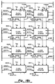
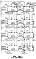
- the networks of Figs. 5 and 6 are preferably composed of identical switches (Fig. 7). Each switch chip forms a self-setting gate that routes requests and responses between four parallel ports on each side of the switch.
- a processing node issues a request which is routed to the node that contains the desired memory location. The node then fetches the desired word from memory, and the response is relayed back through the network following the same path as the original request. Requests and responses are pipelined through the network allowing a new request to be issued from every node every 150 ns, with a network clock period of 25 ns, the same period as the node clock.
- Each network switch may be constructed as a single, 30K gate, CMOS, VHSIC-scale chip. Each request may take three, 25 ns clock cycles to propagate through each switch on both the forward and the response paths.
- the chip can then be used to interconnect systems with up to 1024 processors without modification. The chip is easily modified to handle more than 1024 procesors.
- the switch may incorporate error detection and failure avoidance to enhance system availability.
- the network consists of identical 4 by 4 self-setting switches.
- the network has two types of input/output terminals: Request and response.
- Each processing node in the system has one of each.
- the first two cycles contain node and memory address, while the second 2 cycles hold a swap or fetch-and-add parameter.
- the request is transformed across the network to the addressed node's Response terminal.
- the addressed node fetches the desired memory location, and the data is relayed back through the network to the original request port.
- the fetch-and-add and swap operations require the receiving node to write after reading to modify the memory cell indivisibly.
- the Request and Response terminals are administered by a Network Interface Chip in every node. The Network Interface Chip initiates requests, fetches responses, and modifies the fetch memory location appropriately.
- a two-layered network has an advantage over a fully-layered network for some applications because the two-layered version provides a robust set of possible connections and currently can be constructed with the VHSIC-scale 1.25 micron and packing technology available.
- the network for 64 processing nodes may consist of 448 identical CMOS chips arranged in seven stages of 64 chips each.
- the switch implements the functionality required for Layered Networks with two planes and the number of processing nodes, N, equal to a power of two up to 1024.
- a switch occupies a single VLSI chip.
- the switch has four "inputs" toward the requesters, and four "outputs" toward the responders.
- Each input and output consists of a sixteen bit bidirectional, parallel path augmented with appropriate control signals.
- the switches route requests and responses to those requests in pipelined waves through the network.
- Each switch receives requests on its left-hand terminals, it then calculates its switch setting and parameter modifications, transmits the requests on the appropriate right-hand terminals, records the response switch setting and appropriate fetch-and-add (or "fetch-and-op) or swap parameters. Finally, upon receipt of the responses on the right-hand terminals, it recalls the switch setting and parameters to transmit the possibly modified responses on the appropriate left-hand terminals.
- Switches are set in parallel using only information contained in the requests a particular switch handles. Up to four requests may simultaneously arrive at any particular switch. Each request is checked against its error code and any requests in error are not relayed. If two or more requests have the same destination processing node, memory address and operation, they are combined. Fetch-and-add requests are combined by adding the parameters. Swap requests are combined by choosing one of the parameters and passing it on. In all other circumstances where the destination nodes match, but the operations or memory address don't match, one request takes precedence over the others. Once the switch setting is determined, the requests are transmitted to the next stage of switches. Because the switch settings are stored during request routing, the responses follow the same path through the network, but in the opposite direction, by recalling the original setting.
- Layered Networks may provide two operations, fetch-and-add and swap, to facilitate coordination of concurrent activity.
- the fetch-and-add operation can be used to manage the queues used for job scheduling and data flow buffers.
- the swap operation allows modification of pointers used for dynamic data structures.
- the fetch-and-add operation allows many processors to "read then add" the same memory location simultaneously and receive responses as if the operations had occurred in some sequential order.
- Fetch-and-add allows a job queue pointer to be referenced simultaneously by several users and provides each processor with a different job pointer.
- the swap operation allows manipulation of pointers used in dynamic, shared, data structures.
- the fetch-and-add operation returns the value of the designated memory location, but increments the value left in the memory by adding the fetch-and-add parameter to it. If the memory location is used as a queue pointer, each fetch-and-add reference will return a different value.
- the network allows any or all processing nodes to access the same memory location simultaneously with the fetch-and-add operation and each node gets distinct values returned as if the fetch-and-add operations had occurred in some sequential order. This property allows many procesors to access the job queue simultaneously, and, therefore, keep all processors busy with minimal overhead. Similarly, many reader-many writer data flow queues may be accessed simultaneously by several processing nodes. A simple read of memory is accomplished by a fetch-and-add operation with a parameter of zero.
- the swap operation returns the value of the designated memory location, but replaces the value in memory with the swap parameter.
- the swap operation is intended for manipulation of pointers. For example, insertion of a record into a singly-linked list would perform a swap operation on the pointer of the record after which the new record will be inserted.
- the swap parameter would be the pointer to the new record, and the returned value would be written to the pointer in the new record to continue the list.
- Swap operations are combined in the network to allow any or all processing nodes to swap the same memory location simultaneously and get returned values as if the swap operations had occurred in some sequential order. Swap operation combining allows any number of processing nodes to insert new records into the same list, simultaneously.
- the network switch has four left-hand terminals toward the Requesters, four right-hand terminals toward the Responders, several hard-wired parameters, several clocks, and a maintenance interface.
- Requests are received on left-hand terminals and are routed to right-hand terminals with appropriate modifications to request parameters.
- Responses are received on right-hand terminals and are routed to left-hand terminals with modifications using stored information about the original request routing.
- Requests contain the information used for switch setting. Requests may be combined, deferred, or switched according to their node address, memory address, and request type. Responses contain the possibly modified word stored in the addressed memory location by the associated request. Responses may be modified if their associated requests were combined. Stored response parameters, calculated from request parameters, are added to the responses if the requests were combined. In addition, a response may be split into two or more responses if the associated requests were combined into one.
- Fetch-and-Modify operations such as Fetch-on, Fetch-And, Fetch-Multiply may be used along with swap operations so that parameters may be modified depending on their associated requests. Parameter modification when requests are combined supports the apparent serialization of simultaneous operations necessary for coordination of concurrent processing.
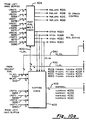
- the left and right-hand switch terminals of the switch 20 are composed of four groups of wires. Each group of wires contains: 16 data wires, two error code wires, and three control wires. The wires are all used bidirectionally.
- the left-hand switch terminals receive requests and transmit responses. Requests are driven in four clock cycles: The first two cycles contain node destination and memory address information; the second two cycles contain the fetch-and-add or swap parameters. Responses are driven in the opposite direction on the same wires in two more cycles. Every switch in the network performs each of these six exchanges in parallel. Therefore, new requests may be issued from the network interface from any or all processing nodes every six clock cycles.
- Each of the four left-hand terminals and four right-hand terminals shown in Fig. 7 consist of 21 bidirectional lines: 16 data, two check code, and three transaction type.
- Fifteen chip pins are used for hard- wired parameters: four for each of the two Bit Pick choices, two for the appropriate address bits of this chip and five for Slider offset.
- the chip pins may be replaced by configuration registers set upon system initialization.
- Seven clocks are used by the chip: a 40 MHz system clock, and six transaction phase clocks which coordinate the six system clock cycle routing of data.
- the seven clocks may be replaced by two: a 40 MHz system clock and a synchronizing clock for deriving the six phases.
- Node and memory addresses for a request are transferred from the right-hand network terminals of one switch to the left-hand network terminals of a switch in the next stage when the two receive-requests clocks are active.
- Parameters for the request (either fetch-and-add or swap), are transferred on the next system cycles in the same direction when the two receive-parameter clocks are active.
- responses to requests are transferred in the opposite direction back to the requesters when the two send-response clocks are active.
- the six transaction clocks ensure orderly transfer of data between switches.
- a switch may simultaneously receive up to four requests on its left-hand network terminals when the receive-request phases are active.
- the two 16-bit data fields are interpreted as 10-bits of node address and 22-bits of memory address.
- a request has a type of either fetch-and-add or swap. Requests with the same node address, memory address and type are combined into a single request. Since each node contains a single-port memory, only one memory address may be accessed at a time. Therefore, two, (or more), requests with the same node address, but different memory addresses cannot be combined, and, therefore, only one request is transferred to the next stage as the others are deferred.
- the rules for message combining or deferral are as follows:
- the switch can place requests on either of two "planes" of connections to the next stage. Each of the planes of Figs. 5 and 6 correspond to one bit of the node address of the requests.
- the switch may place requests on a "straight" or "crossed" terminal on either plane.
- a straight terminal connects to the switch in the next stage that has the same switch-number.
- the cross terminals connect to a switch in the next stage that has the same switch-number, except for a single bit, the bit corresponding to the plane.
- the bits corresponding to the planes are identified for the chip by two hard-wired 4-bit parameters. Those two bits are extracted from the node address of each request. The bits are compared with two bits of the switch-number that are hard-wired. If the extracted bit of a request differs from the corresponding hard- strapped bit, the crossed terminal on that plane will bring the request closer to the addressed node. Whether either of the cross terminals are helpful is used to claim the right-hand terminals.
- a set of four adder trees are used for routing and combining. Each adder tree can select to add any or all of the four data fields of the four requests. When the requests are switched, the adder trees act like simple selectors. Each tree is associated with one of the right-hand terminals. Each tree selects the request that claimed its right-hand terminal and adds zero to it. Finally, the requests are transmitted on the right-hand terminal to the next stage.
- the request parameters following each request when the receive-parameter phases are active, are routed somewhat differently.
- the right-hand terminal to be used has already been determined. However, the parameters may be added if two or more requests were combined.
- the parameters of all fetch-and-add combined requests are added to form the parameter for the combined request.
- the parameter from the lowest numbered left-hand terminal is selected when requests are swap combined.
- the adder trees are also used to compute response parameters to be used when the response is received.
- the response to a fetch-and-add request that was combined in the switch must be modified so that each combined request gets data as if the requests occurred sequentially.
- the stored parameters will be added to the response during response routing.
- the parameter is the sum of all the fetch-and-add combined request parameters coming from lower numbered left-hand terminals.
- swap requests When swap requests are combined, one of the parameters is sent on while the others are saved. Upon receipt of the response, the response is sent unmodified for one of the requests while the others take the request parameter of one of the swap combined requests.
- the swap parameter for each combined request is the parameter of the request coming from the next largest left-hand terminal, or zero if this is the largest.
- the requests and their parameters reach the desired node.
- the memory location is fetched and the value is returned on the network as a response.
- Responses are transferred from left-hand terminals to right-hand terminals of the previous stage when the send-response is active.
- Each switch retains a parameter and response switch setting in a ram file configured to behave like a shift-register.
- a ram file, called Slider uses a parameter called Stage-Delay to determine the length of the apparent shift register. This value is hard-wired to be approximately the number of stages to the right-hand side of the network. (See section 7.c. of the switch chip specification section of this paper for the exact formula.)
- the Slider automatically presents the required parameters and response switch setting when the responses are latched into the switch from its right-hand terminals.
- the response switch setting and response parameter calculated during the request routing and stored in Slider vary according to whether the requests were combined, deferred, or switched unmodified.
- the response switch setting selects one of the response data words or zero to be added to the stored parameter.
- the type associated with the response is selected, or substituted with a type indicating the request was deferred.
- the rules governing response switch setting are as follows:
- the possible modified request types and data word are transmitted from the left-hand terminals when the send-response phases are active.
- the Network Switch routes requests and responses through the switch in six 25 ns clock cycles.
- the switch combines fetch-and-add or swap requests, and splits the response.
- Request combining allows many processing nodes to fetch-and-add or swap the same memory location and receive responses as if each of the requests had occurred sequentially.
- the network latency is low since the requests and responses require only three clock cycles to traverse each switch in each direction and the throughput is high because the requests and responses are pipelined through the network, a new request can be issued from every processing node every 150 ns.
- a key feature of the Layered Network interconnect is its ability to combine compatible requests into combined requests that can be satisfied en masse at the responding node, in the same network transmission time as for individual requests.
- the simplest example of this effect is the broadcast read, where several processors happen to simultaneously request a read of the same memory cell.
- Each switch involved in the broadcast combines two or more such requests into a single request to be sent on, and remembers the occurrence of the coincidence. When the read data returns, the switch copies it to each of the original incoming requests.
- the same principle can be applied to more complex requests.
- the essential requirement is that the request be combinable in any order, and the combination be representable in a single request. Given such requests, they may be applied to shared memory locations without time consuming conflicts in either the network or the node that contains the memory location. Programs that reference such locations must be prepared to deal with them occurring in any order, which is the essence of multitasking. In turn, the network and node memory assure that there is an equivalent serial order, that is, some serial order of the operations that would cause the same resulting values in the memory cell and all of the tasks.
- Request combinations can be easily defined for memory reads and writes.
- the class of arithmetic and logical operations called "fetch-and-op" has been described in the literature. [See “Issues Related to MIMD Shared-Memory Computers: The NYU Ultracomputer Approach, The 12th Annual Symposium on Computer Architecture," 1985, p. 126] It defines operations in which the memory cell contents are modified by an associative operation such as ADD or AND. The value of the memory cell before modification is returned to the requester. The swap operation replaces the memory cell contents with the request's supplied data, returning the memory cell's original contents. This operation is not associative, though it is straightforward for the network to guarantee an equivalent serial order for combined requests. Nonassociativity means that the software using the swap operations must be prepared to deal with the possible different orderings.
- Latency and throughput are critical requirements of a concurrent system. Since a new request can be issued every six clock cycles or 150 ns, 6.6 million, requests can be issued and responses received by each node every second. For a 64-node system, the network can transport 53 billion bits per second (40 MHz 64 nodes * 21 bits per port). Although the throughput of the network grows linearly with the number of processors, the network latency grows logarithmically with added nodes. The latency of a message, (the time from request issue to response receipt), is the sum of the request routing, memory access, and response returning. A 64-processor system would have seven, (logN + 1) columns of switches, each column imposing one network of delay (six clock cycles total) for request and response routing.
- the total latency for a 64 processing node system would be 1200 ns.
- the excellent latency and throughput provided by the network allows the high-speed communication required to effectively utilize the processing power gained by adding processors.
- the following chip specification for the Layered Network sets forth pin connections, formatting, timing and the manner in which requests are combined, decombined and routed (for example, by use of fetch-and-add and swap operations).
- the total pin count is: 213 including power and ground.
- the request from the originating node needs to be split into 4 parts.
- the switch chip samples the lines on the negative edge of the controlling clock phase (RCV_REQ A (301), etc.).
- the left hand terminals of the switch chip need to see:
- the response is sent out from the left hand terminal to the previous stage during the following clock phases:
- the command type consists of 3 bits.
- the 2 least significant bits indicate the command type and the most significant bit is for odd parity.
- the types are:
- Handshaking between stages occurs on the type lines (309A-D, 548A-D).
- the possible handshake states are: The handshake is put out to the previous stage by the left hand terminals during RCV_PARAM A (303) and RCV_PARAM_B (304) and is sampled from the next stage by the right hand terminals on the negative edge of SND_RESP_B (306) and RCV_REQ_A (301).
- EFPLO (330) is the effective plane for plane 0 and can take on any value from 0 to 9.
- EFPLO (330) is the bit location in the node address that plane 0 is working on. Example: If plane 0 is switching based on the value of bit 6 in the node address then EFPLO (330) would be wired as a 6.
- EFPL1 (331) is the same except that it is the effective plane for plane 1.
- DIGITO (332) is bit EFPLO (330) of the switch number.
- the STAGE_DELAY (610) pins are used to tell the switch chip how long to wait before expecting to see the response come back for the current request. There are log 2 (N) + 1 stages (columns) of switches in the network for N nodes.
- stage is the column number the switch is in the network.
- Stage can take on values from 0 to log 2 (N).
- the left hand side of the network (left most) is stage 0 and the right hand side (right most) is stage log2 (N).
- Memory_access_cycles is the number of network clocks a request needs for access to the same memory location. A new request comes along every 6 network clocks. Within those 6 network cycles the memory location must be read out, corrected for errors, a MOD 3 calculation done, modified according to fetch-add or swap, a new syndrome calculated and finally, written back to the same memory location. (An alternative is to not do correction on the response, but just issue a memory error if an error occurrs.
- Memory_access_cycles must be less than or equal to 6 in order for the memory to finish the current request before the next request comes along. Other_cycles includes the time it takes to go both ways through any network interface chip and any other pipelining or delays. All Other_cycles must consist of a pipeline. Time is measured in network clock cycles. (Memory_access_cycles + Other_cycles) is the total time between the leading edge of the request leaving the right hand side of the network and the leading edge of the response coming back to the right hand side of the network. (Memory_access_cycles + Other cycles) can ONLY take on the following values:
- the RESET (611) pin must be brought HIGH and held HIGH while the Slider Reset Control (613) steps through the 32 RAM addresses.
- the RAM (RAM_LS 603, RAM_MS 606) in the Slider (103) must be initialized, therefore the RESET signal cannot be asynchronous with CLOCK.
- the second set of requests during times 14 to 21 consists of 4 Swaps that go to the same destination node and memory address. They are:
- the third set of requests during times 26 to 33 consists of 2 Fetch adds and 2 Swaps. They are:
- the order of priorities is than plane 1 is always preferred over plane 0.
- Cross connected terminals are preferred over straight connected terminals if the request wants a cross connected terminal. If a request does not want any cross connected terminals (meaning it wants a straight connected terminal) and no straight connected terminals are available then a cross connected terminal is chosen with plane 0 being preferred because at the next stage there is a chance to get back on using the "catch up" plane. If all other things are equal then an arbitrary decision is made to give the lower numbered left hand terminal's request priority.
- Plane 1 is the catch up plane so any request that wants plane 1 has to get it now because there is not another chance to get it, unless you are at the first stage in which case there is a second chance for the catch up plane at the last stage.
- Plane 0 is the main plane. The next stage has the same effective plane as the catch up plane so there is a second chance to get routed.
- EFPLO (330) : 9
- the destination node address is: 11 0000 0000 (binary) (C000 0000 HEX).
- DIGITO (332) does not match bit 9 of the destination node address so the request wants plane 0 crossed.
- DIGIT1 (333) matches bit 0 of the destination node address so the request does not want plane 1 crossed.
- the combined request ends up getting plane 0 crossed (RHNTDT1, 546B).
- the switch chip stores the return path and parameters that must be used to route and decombine the responses.
- the return paths and the stored response parameters are stored in locations according to which left hand terminal the request came in one.
- the return path value is the right hand terminal the request went out on. See the section on combining requests, decombining responses for examples of the return path and the stored response parameters.
- the switch chip performs error detection on the requests and responses as they go through the chip. If an error occurs then the request is stopped if the request has not already left the chip and the response type for that request is forced to an error condition. If an error is detected after a right hand terminal has been claimed then the request is allowed to go through, but the response is stored as a force error response.
- the hardwired connections for each switch chip are:
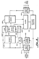
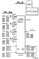
- Fig. 8 shows an overall block diagram of a chip for a switch 20.
- Up to four requests can come from the previous stage into the Left Hand Buffer (100).
- the incoming "requests" are forward routed to the correct right hand terminal and combined if possible.
- the requests then go out to the next stage through the Right Hand Buffer (105).
- the Slider (103) saves the reverse switch settings and the stored response parameter for decombining thr responses to requests that were combined.
- the responses come back from the next stage through the Right Hand Buffer (105) and go into Response Reverse Routing-Decombining (104).
- the responses are routed to the proper left hand terminal and are decombined if necessary.
- the responses then go to the previous stage through the Left Hand Buffer (100).
- the Error Control Block (101) monitors the four paths through the chip, records error occurrences, and if too many errors occur on a particular path, then that path is shut off and all data must be routed through the remaining paths.
- the circuit labelled Bit Pick (200) examines the node address of requests and determines which right hand terminal each request wants.
- Request Evaluation (201) compares each request with every other request and determines whether requests can be combined and which requests have priority over other requests. Request Evaluation (201) also checks for MOD 3 errors on the data paths.
- the Claim Section (202) compares the wanted right hand terminals with the priorities of each request and assigns a right hand terminal to each request.
- the Snap Register (204) saves data between clock phases for future use.
- Switch Setting (203) takes the assigned right hand terminals and the combinability information and sets up the control lines to the Selective Adders (205) to route and combine the requests to the correct right hand terminal. Switch Setting (203) also sets up the Selective Adder control lines for calculating the stored response parameter for response decombining. Switch Setting (203) also calculates the reverse switch setting for routing the response through the Response Selector (104). If there were not enough working right hand terminals for all of the requests, then instead of saving the reverse switch setting in the Slider (103) a Force Error Response bit is set in the Slider signifying that the request was not routed. The Selective Adders (205) are used for routing the request, routing and calculating the forward parameter and calculating the stored response parameter.
- Figs. 9-26 show detailed block diagrams of the Network Switch. All blocks that are labelled LATCH are feed-through latches. Data is fed through to the output when the clock is high and the output is held when the clock is low.
- the Left-Hand Buffer (100) (which includes the bidirectional I/O control circuits 310A-310D) 16 bits of request data (LHNTDT_, 307A-D) and 2 bits of check codes for the data (LHNTCC_, 308A-D) are accepted from the previous stage during clock phases RCV_REQ_A (301), RCV_REQ_B (302), RCV_PARAM_A (303) and RCV PARAM_B (304).
- Response data and check codes are sent to the previous stage on the same lines during clock phases SND_RESP_A (305) and SND RESP_B (306).
- 3 bits of request type (LHNTTY_, 309A-D) are accepted from the previous stage during clock phases RCV_REQ_A (301) and RCV REQ_B (302).
- the response type is sent to the previous stage during clock phases SND_RESP_A (305) and SND_RESP_B (306).
- a handshake 'valid request received' (314A-D) is sent to the previous stage on the type lines (309A-D) during clock phases RCV_PARAM_A (303) and RCV PARAM_B (304).
- the Left Hand Buffer Handshake circuits (315A-D) are shown in Fig. 26.
- the Handshake circuits check that the received type has odd parity and puts out a 4 if the parity is odd and a 7 if parity is even (indicating error).
- the upper 10 bits of the data lines (LRQDT_[6..15], 327E-H) are sent to Bit Pick (200) to determine which right hand terminals are wanted (338A-H). These 10 bits represent the Destination Processor Address during RCV_REQ_B (302). Only the cross-connected right hand terminals have 'want' signals. The straight-connected right hand terminals are the default if no crossed terminals are wanted by a request.
- Fig. 14 shows the details of Bit Pick. 10:1 muxes within Bit Pick select one bit of the Destination Processor Address using EFPLO (330) or EFPL1 (331) as control lines to designate the effective planes.
- the selected bit is then EXCLUSIVE-ORED with either DIGITO (332) or DIGIT1 (333) to produce REQ_WANT_ (338A-H).
- LRQDT_[6..15] (327E-H) is also sent to a 10 bit Equality Checker (335) to see if any 2 destination processor addresses are equal.
- the signals produced are PA_EQ_ (340A-F).
- the full 16 bits of data (LRQDT_, 327A-D) are sent to a 16 bit Magnitude Comparator (336) to find out which memory addresses are equal (MA_EQ_ 341A-F) and which memory addresses are greater than other memory addresses (MA_GT_, 342A-L).
- the magnitude comparison is only valid during RCV_REQ_B (302) and RCV_PARAM_A (303).
- a MOD 3 check is done on the data (LRQDT_, 327A-D) and compared to the check codes (LRQCC_, 328A-D) within the block Request Evaluation MOD 3 Check (404).
- the MOD 3 checker assembly (Fig. 15) consists of a tree of 2 bit MOD 3 adders. The first row of the tree is a special reduced MOD 3 adder to handle the conversion of a 16 bit binary number to sets of 2 bit MOD 2 numbers. Logic of the MOD 3 adders is shown in Fig. 24. Within the Request Evaluation MOD 3 Check block a further check on the type lines is done. The request types are decoded within Suspend Check (405) into either Fetch add or Swap (TY_ISFA, 400A-D and TY_ISSW, 400E-H).
- Type decoding is shown in Fig. 16. If the type is not either Fetch_add (i.e., fetch-and-add) or Swap, then that request's DT OK (402A-D) line is brought low indicating that the data is to be ignored. Either there has been an error or there is no request.
- the complement of the DT OK (402A-D) lines is RQE_ER_ (401 A-D) and are sent to Error Control for monitoring the errors on each path through the chip.
- Suspend Check (405) checks to see if a request needs to be suspended either because there has been an error in a request or a request has low priority and the same destination processor address as a higher priority request, but cannot be combined with that higher priority request.
- Suspend Check logic is shown in Fig. 16. A smaller memory address has priority over a larger memory address. Swap has priority over Fetch add.
- SUSPEND_ (403A-D) is then sent to Merge Check (452) and Req_active (453). Merge Check compares each request with every other request and sees which requests can be combined into one.
- Fig. 23 shows the logic for Merge Check and Req_active. Requests are combined only if their destination processor addresses are equal, their memory addresses are equal, their types are equal and they have not been suspended. Req active (453) determines which requests are active after combining takes place. In a set of combined requests, the one with the lowest numbered left hand terminal is the one that remains active and in control of the combined request. Requests that are not combined and not suspended are also active. Since the request is split into 2 halves (multiplexed to limit the external pin count) a comparison must be made between the 2 halves of the request to see if the decision made during the first half is still valid during the second half. AND gate groups 454 and 455 compare the merge signals of the first half with the second half.
- AND gate group 456 (REQ_ABORT, 429A-C) checks to see if a REQ_ACTIVE (408A-D) signal was aborted due to conflicting memory addresses on a previous merge or conflicting types or errors on the second half of the request. There is no REQ3_ABORT since request 3 is never active if it is merging with another request.
- AND gate group 457 (REQ_NEW, 430A-C) checks for a new request being active during the second half when it was not active during the first half. A REQ_NEW line will go high if the lowest numbered request in a group of requests that are being merged is suspended during the second half of the request.
- the request arriving on left-hand terminal 0 would always be the controlling request during the first half of the request.
- the request has the highest priority.
- the MERGE, ABORT, and NEW signals are sent to New Controlling Request (437) to determine which request was in control, the first half versus which request is in control during the second half.
- the logic for New Controlling Request (437) is shown in Fig. 17.
- the output signals are R_NEW_ (436A-I) where the number before the NEW indicates the old controlling request and the number after the NEW indicates the new controlling request.
- the Claim Matrix (202) assigns right hand terminals to requests. Error Control can disable a right hand terminal by bringing one of the lines POSBAD, POCBAD, P1 SBAD or P1 CBAD (600A-D) high.
- the Claim Matrix uses the REQ_WANT_ (338A-H) and REQ_ACTIVE (408A-D) lines to assign right hand terminals.
- the Claim Matrix is shown in Fig. 18.
- the Claim Cell is shown in Fig. 22.
- the order of priority in assigning right hand terminals is plane 1 crossed (P1 C), plane 0 crossed (POC), plane 1 straight (P1 S) and plane 0 straight (POS).
- This priority scheme is represented by the order of the columns in the Claim Matrix. If a request did not want a crossed terminal and both of the straight terminals are already claimed, then that request is going to get a crossed terminal from the last 2 columns of the claim matrix. The priority order is plane 0 crossed and then plane 1 crossed. Plane 0 crossed is given priority because at the next stage the request will want plane 1 crossed and be able to get back on track by using the "catch up" plane.
- the order of the rows indicates the priority of the requests based on left hand terminal number. If all other things are equal, then the request arriving on the lower numbered left hand terminal has priority.
- the column priority order takes precedence over the row priority order. Wanting a crossed right hand terminal has higher priority than being a lower numbered left hand terminal.
- the outputs of the Claim Matrix are R_GET_(417A-P).
- HR_GET_ (419A-P) and R_NEW_ (436A-I) are fed to New Got Its (438) to determine how to reassign the right hand terminals during the second half of the request. It is not sufficient to merely redo the claims with the Claim Matrix during the second half because the priorities between requests may have changed due to aborts during the second half. If the priorities change and the claims are redone, then a request may be split between 2 right hand terminals. Example: if requests 0, 2 and 3 are being combined and want plane 1 crossed and request 1 goes through by itself and also wants plane 1 corssed, then at the end of the first half of the request, request 0 will get plane 1 crossed and request 1 will get plane 1 straight.
- the Snap Register (204) is used to hold data for use in future clock phases.
- Register 420 holds the types SNTY_ (421A-D).
- Register 424 holds the first half of the parameter's data and check bits. The second half of the parameter's data and check bits is held in the Left hand Buffer Registers 324A-D and 325A-D. The first and second half of the parameter is multiplexed (446) into Register 451 producing the signals SNDT_ (449A-D) and SNCC_ (450A-D) which are then sent to the Selective Adders (205, 520).
- the reason for the Snap Register is that the request parameter needs to be used twice: once for calculating the forward parameter and once for calculating the stored response parameter.
- both halves of the parameter flow through terminal 0 of the mux (446).
- the stored response parameter the first half of the parameter comes from terminal 1 of the Mux (446) and the second half of the parameter comes from terminal 0 of the Mux (446).
- Register 433 saves the merge signals SNR_FA_ (434A-F) and SNR_SW_ (435A-F) for future use.
- Stored Response Parameter Selective Adder Switch Setting (502) takes the merge signals SNR_FA_ (434A-F) and SNR_SW_ (435A-F) and determines how to set up the Selective Adders for calculating the stored response parameter.
- the logic for the Stored Response Parameter Selective Adder Switch Setting (502) is shown in Fig. 20. If a request is not being combined with any other request, then the stored response parameter is 0. If a request is being Fetch_add combined with other requests, then the stored response parameter is the sum of the parameters of the other requests being combined that have lower left hand terminal numbers. If the request has the lowest left hand terminal number of those requests being combined, then the stored response parameter is 0.
- the stored response parameter is the parameter of the request (among those being combined) with the next higher left hand terminal number. If the request has the highest left hand terminal number of those requests being combined, then the stored response parameter is 0.
- Selective Adder Switch Setting takes the signals SNR_FA_ (434A-F), SNR_SW_ (435A-F), NEW_R_GET_(445A-P) and HF_ADD_ (509A-P), (Stored Response Parameter Selective Adder Switch Setting) and produces the signals that control the Selective Adders: F ADD_ (515A-P).
- F_ADD_ the number before the ADD indicates the left hand terminal number and the number after the ADD indicates the right hand terminal number.
- the logic for Selective Adder Switch Setting (514) is shown in Fig. 20.
- RCV_PARAM_A (303) and RCV_PARAM_B (304) the request is routed through the Selective Adders based purely on which right hand terminal the request got. No addition takes place.
- SND_RESP_A (305) and SND_RESP_B (306) the forward request parameters are calculated.
- the parameter is routed through the Selective Adder based on which right hand terminal the request got. If the request is being Fetch_add combined with other requests, then the forward parameter is the sum of all of the parameters being combined. If the request is being Swap combined with other requests, then the forward parameter is the parameter of the request with the lowest numbered left hand terminal.
- RCV_REQ_A (301) and RCV_REQ_B (302) the stored response parameter is calculated as described above.
- Response Selector Switch Setting (501) calculates the right hand terminal that each request actually went out on based on the Merge signals SNR_FA_ (434A-F), SNR_SW_ (435A-F) and the New Got Its NEW_R_GET (445A-P).
- the logic for Response Selector Switch Setting (501) is shown in Fig. 19.
- the assigned right hand terminal is encoded in the 2 low order bits of B_SEL (513A-D).
- the high order bit of B_SEL (513A-D) is set if a request did not go out on any right hand terminal due to conflicts or errors.
- the high order bit is used to force an error response when the response comes back through the chip.
- the Response Selector Switch Setting bits are saved in the Slider (103) for use in reverse routing the response.
- Force Zero Add (500) is used for control when decombining a response that was Swap combined.
- the logic for Force Zero Add (500) is shown in Fig. 17.
- the original request with the highest numbered left hand terminal will get the response parameter that comes into the Right Hand Buffer (105).
- the other requests will ignore the response coming from the Right Hand Buffer (105) and use their stored response parameters based on the Force Zero Add bits ZE_ (512A-D).
- the Force Zero Add bits are saved in the Slider (103) for use when the response comes back.
- the Selective Adders (205) are used for routing the request, routing and calculating the forward parameter and calculating the stored response parameter as described above. Since the parameters are split into two halves, carry bits are saved between halves by Register 522.
- the Selective Adders consist of 4 sets of adders each of which can add together any combination of the 4 input data lines (SNDT_, 449A-D). Since up to 4 operands can be added together, there needs to be 2 carry bits per adder set.
- the logic for the Selective Adders is shown in Fig. 11 and 21.
- the check codes for the operands that were added are added using MOD 3 adders.
- the carry bits from the first half of the addition (HCARRY_, 521A-H) are added into the check code using a Special MOD 3 Adder (Fig. 24).
- the stored carry bits, HCARRY_ (21A-H)
- the current carry bits (CARRY_, 524A-H) from the Selective Adders are added in a special MOD 3 Adder and then MOD 3 subtracted from the check codes to produce the final check codes FSWCC_ (529A-D). This is necessary for the check codes for each of the sixteen-bit halves of the parameter to remain correct in the presence of carries.
- a MOD 3 Subtractor is shown in Fig. 25.
- the request types are routed along with the request during RCV_PARAM_A (303) and RCV_PARAM_B (304) and are ignored at all other times.
- AND gate group 2018 (Fig. 21) puts out 'no request' if no request is using that particular right hand terminal.
- the routed request types are FSWTY_ (530A-D).
- the routed data signals are FSWDT (528A-D).
- Fig. 11 the output of the Selective Adders (520) goes to two registers.
- One register (536) feeds the request and forward parameter to the Right Hand Buffer (105) and the other register (535) feeds the stored response parameter to the Slider (103).
- the Right Hand Buffer (105) sends the data and check codes out to the next stage during RCV_PARAM_B (304), SND_RESP_A (305), SND_RESP_B (306) and RCV_REQ_A (301). Note the 3 phase offset between the request coming into the Left Hand Buffer (100) and the request going out of the Right Hand Buffer (105).
- the response data and check codes are accepted from the next stage during RCV_REQ_B (302) and RCV_PARAM_A (303).
- the request type is sent out to the next stage during RCV_PARAM_B (304) and SND_RESP_A (305).
- Handshake signals are accepted from the next stage on the type lines during SND_RESP_B (306) and RCV_REQ_A (301).
- the response type is accepted from the next stage during RCV_REQ_B (302) and RCV_PARAM_A (303).
- the Handshake logic (557) is shown in Fig. 26. If a handshake error occurs, then Error Control (101) is notified via the lines HANDERR_ (559A-D) that a path has a problem.
- the Slider (103) consists of 2 sections of RAM and is shown in Fig. 12.
- the first section, RAM_LS (603), is 88 bits wide and 32 words deep.
- the second section, RAM_MS (606), is 72 bits wide and 32 words deep.
- the Slider Reset Control (613) loads binary 100 (4 decimal) into all B_SEL (513A-D) locations and 0 into all other RAM locations when RESET (611) is active.
- the binary 100 indicates 'no request'.
- the Slider Reset Control (613) works by stepping through all 32 addresses of the RAM_(603, 606), forcing the data lines (512, 513A-D, 537A-D, 538A-D) to the correct values and activating the Write-Enable Lines (602, 605) during each address.
- the Read Counter is initialized to 0 and the Write Counter is initialized to STAGE_DELAY (610) when RESET (611) is active.
- the Read and Write Counters are always offset by STAGE_DELAY (610) during the entire operation of the Switch Chip.
- STAGE_DELAY (610) indicates when the response is expected to come back to the Switch Chip on the Right Hand Buffer.
- RAM_LS (603) saves the Force Zero Add bits (ZE_, 512A-D), the Reverse Switch Settings (B_SEL, 513A-D), and the first half of the stored response parameter (HFSWDT_, 537A-D and HFSWCC_, 538A-D) during RCV_REQ_B (302).
- the second half of the stored response parameter is saved in RAM_MS (606) during RCV_PARAM_A (303).
- the stored information is read out during SND_RESP_B (306) and saved in a register (627) for future use. The data is read out early and saved to avoid a conflict with writing to the RAM_ (603, 606).
- the least significant (first) half of the stored response parameter is sent to the Response Selector (104) and used during RCV_PARAM A (303).
- the most significant (second) half of the stored response parameter is sent to the Response Selector (104) and used during SND_RES_A (305).
- the reason for calculating the 2 halves of the response during non-contiguous clock phases is to save a register in the Left Hand Buffer (100).
- the Response Selector (104) logic is shown in Fig. 13.
- the data (LRSDT_, 554A-D) from the Right Hand Buffer (105) is routed to the correct left hand terminal (MUX_DT_, 704A-D) by MUX (703) based on the Reverse Switch Setting bits from the Slider (SLSS_[0..1], 629A-D). If the Force Zero Add bit (SLZE_, 628A-D) is set, then the data from the right-hand buffer (105) is ignored.
- the routed data (MUX DT 704A-D) is added by 16 bit Adder (717) to the stored response parameter (SLDT_, 635A-D). Carries are saved between halves of the response (HCARRY , 725A-D).
- the outputs of the Adders (717) are saved in register (716) and are sent to the Left Hand Buffer (100) as HRSDT_ (700A-D).
- the check codes (LRSCC_, 555A-D) are similarly routed to the correct left hand terminal (MUX_CC_, 706A-D).
- the check codes are MOD 3 added to the stored check codes (SLCC_, 636A-D) and are added to the stored carry bits (HCARRY_, 725A-D).
- the current carry bits (CARRY_, 719A-D) are MOD 3 subtracted from the check codes.
- the check codes are saved in register (716) and sent to the Left Hand Buffer (100) as HRSCC_ (701 A-D).
- the Response Selector (104) also does a MOD 3 check (Fig. 15) on the incoming data paths (554A-D, 555A-D). Any error is routed to the correct left hand terminal with the Mux (731) where it forces an error response at the type routing Mux (735). The response type is routed to the correct left hand terminal with the Mux (735).
Landscapes
- Engineering & Computer Science (AREA)
- Computer Hardware Design (AREA)
- Computer Networks & Wireless Communication (AREA)
- Theoretical Computer Science (AREA)
- Physics & Mathematics (AREA)
- General Physics & Mathematics (AREA)
- Software Systems (AREA)
- General Engineering & Computer Science (AREA)
- Mathematical Physics (AREA)
- Signal Processing (AREA)
- Data Exchanges In Wide-Area Networks (AREA)
- Multi Processors (AREA)
- Telephonic Communication Services (AREA)
- Computer And Data Communications (AREA)
- Small-Scale Networks (AREA)
- Use Of Switch Circuits For Exchanges And Methods Of Control Of Multiplex Exchanges (AREA)
Abstract
Claims (7)
Applications Claiming Priority (2)
| Application Number | Priority Date | Filing Date | Title |
|---|---|---|---|
| US07/108,514 US4833468A (en) | 1987-10-14 | 1987-10-14 | Layered network |
| US108514 | 2002-03-29 |
Publications (2)
| Publication Number | Publication Date |
|---|---|
| EP0334954A1 EP0334954A1 (fr) | 1989-10-04 |
| EP0334954B1 true EP0334954B1 (fr) | 1993-04-21 |
Family
ID=22322642
Family Applications (1)
| Application Number | Title | Priority Date | Filing Date |
|---|---|---|---|
| EP89900410A Expired - Lifetime EP0334954B1 (fr) | 1987-10-14 | 1988-10-14 | Reseau en couches |
Country Status (5)
| Country | Link |
|---|---|
| US (1) | US4833468A (fr) |
| EP (1) | EP0334954B1 (fr) |
| JP (1) | JPH02501183A (fr) |
| DE (1) | DE3880478T2 (fr) |
| WO (1) | WO1989003566A2 (fr) |
Families Citing this family (39)
| Publication number | Priority date | Publication date | Assignee | Title |
|---|---|---|---|---|
| US5088032A (en) * | 1988-01-29 | 1992-02-11 | Cisco Systems, Inc. | Method and apparatus for routing communications among computer networks |
| US5163149A (en) * | 1988-11-02 | 1992-11-10 | International Business Machines Corporation | Combining switch for reducing accesses to memory and for synchronizing parallel processes |
| US5258752A (en) * | 1988-11-25 | 1993-11-02 | Sumitomo Electric Industries, Ltd. | Broad band digital exchange |
| US5123011A (en) * | 1989-09-27 | 1992-06-16 | General Electric Company | Modular multistage switch for a parallel computing system |
| WO1991014326A2 (fr) * | 1990-03-05 | 1991-09-19 | Massachusetts Institute Of Technology | Reseaux de commutation comprenant des groupes logiques extensibles et/ou dispersifs pour acheminer des messages |
| US5216420A (en) * | 1990-07-12 | 1993-06-01 | Munter Ernst A | Matrix sorting network for sorting N inputs onto N outputs |
| US5144293A (en) * | 1990-12-18 | 1992-09-01 | International Business Machines Corporation | Serial link communication system with cascaded switches |
| US5321813A (en) * | 1991-05-01 | 1994-06-14 | Teradata Corporation | Reconfigurable, fault tolerant, multistage interconnect network and protocol |
| US5307413A (en) * | 1991-07-19 | 1994-04-26 | Process Software Corporation | Method and apparatus for adding data compression and other services in a computer network |
| EP0598027A1 (fr) * | 1991-08-05 | 1994-05-25 | Honeywell Inc. | Crossbar comprenant un reseau de retour pour un systeme de commutation et d'acheminement de message sans blocage, a acheminement autonome et pouvant etre mis a l'echelle |
| US5701120A (en) * | 1992-12-13 | 1997-12-23 | Siemens Business Communication Systems, Inc. | Partitioned point-to-point communications networks |
| JP3094849B2 (ja) * | 1995-06-21 | 2000-10-03 | 株式会社日立製作所 | 並列計算機およびその多段結合網 |
| KR100278016B1 (ko) * | 1995-12-26 | 2001-01-15 | 윤종용 | 비동기 전송모드 교환시스템의 스위칭 장치 및 방법 |
| US5867649A (en) * | 1996-01-23 | 1999-02-02 | Multitude Corporation | Dance/multitude concurrent computation |
| US5787081A (en) * | 1996-05-13 | 1998-07-28 | Lockheed Martin Corporation | Allocation of node transmissions in switching networks used with scalable coherent interfaces |
| US5790524A (en) * | 1996-05-13 | 1998-08-04 | Lockheed Martin Corporation | Detection of lost packets in switching networks used with scalable coherent interfaces |
| US5787082A (en) * | 1996-05-13 | 1998-07-28 | Lockheed Martin Corporation | Identification of new and stale packets in switching networks used with scalable coherent interfaces |
| US5826028A (en) * | 1996-05-13 | 1998-10-20 | Lockheed Martin Corporation | Initialization of switching networks for use with a scalable coherent interface |
| FI103312B (fi) * | 1996-11-06 | 1999-05-31 | Nokia Telecommunications Oy | Kytkentämatriisi |
| US6018523A (en) * | 1997-10-22 | 2000-01-25 | Lucent Technologies, Inc. | Switching networks having improved layouts |
| US6215786B1 (en) | 1998-04-06 | 2001-04-10 | Lockheed Martin Corporation | Implementation of multi-stage switching networks |
| US6301247B1 (en) * | 1998-04-06 | 2001-10-09 | Lockheed Martin Corporation | Pad and cable geometries for spring clip mounting and electrically connecting flat flexible multiconductor printed circuit cables to switching chips on spaced-parallel planar modules |
| US6529983B1 (en) | 1999-11-03 | 2003-03-04 | Cisco Technology, Inc. | Group and virtual locking mechanism for inter processor synchronization |
| US6418526B1 (en) | 1999-11-15 | 2002-07-09 | Ncr Corporation | Method and apparatus for synchronizing nodes in massively parallel systems |
| US6519697B1 (en) | 1999-11-15 | 2003-02-11 | Ncr Corporation | Method and apparatus for coordinating the configuration of massively parallel systems |
| US6745240B1 (en) | 1999-11-15 | 2004-06-01 | Ncr Corporation | Method and apparatus for configuring massively parallel systems |
| US6412002B1 (en) | 1999-11-15 | 2002-06-25 | Ncr Corporation | Method and apparatus for selecting nodes in configuring massively parallel systems |
| US6892237B1 (en) * | 2000-03-28 | 2005-05-10 | Cisco Technology, Inc. | Method and apparatus for high-speed parsing of network messages |
| US6505269B1 (en) | 2000-05-16 | 2003-01-07 | Cisco Technology, Inc. | Dynamic addressing mapping to eliminate memory resource contention in a symmetric multiprocessor system |
| US6836815B1 (en) * | 2001-07-11 | 2004-12-28 | Pasternak Solutions Llc | Layered crossbar for interconnection of multiple processors and shared memories |
| US7177301B2 (en) * | 2001-12-27 | 2007-02-13 | Intel Corporation | Signal permuting |
| US7474657B2 (en) * | 2002-04-30 | 2009-01-06 | University Of Florida Research Foundation, Inc. | Partitioning methods for dynamic router tables |
| US7523218B1 (en) | 2002-04-30 | 2009-04-21 | University Of Florida Research Foundation, Inc. | O(log n) dynamic router tables for prefixes and ranges |
| US20040018237A1 (en) * | 2002-05-31 | 2004-01-29 | Perricone Nicholas V. | Topical drug delivery using phosphatidylcholine |
| US7444318B2 (en) * | 2002-07-03 | 2008-10-28 | University Of Florida Research Foundation, Inc. | Prefix partitioning methods for dynamic router tables |
| US7509300B2 (en) * | 2002-07-03 | 2009-03-24 | University Of Florida Research Foundation, Inc. | Dynamic IP router tables using highest-priority matching |
| US7801156B2 (en) * | 2007-04-13 | 2010-09-21 | Alcatel-Lucent Usa Inc. | Undirected cross connects based on wavelength-selective switches |
| US8065433B2 (en) | 2009-01-09 | 2011-11-22 | Microsoft Corporation | Hybrid butterfly cube architecture for modular data centers |
| GB2474446A (en) * | 2009-10-13 | 2011-04-20 | Advanced Risc Mach Ltd | Barrier requests to maintain transaction order in an interconnect with multiple paths |
Family Cites Families (10)
| Publication number | Priority date | Publication date | Assignee | Title |
|---|---|---|---|---|
| SE381548B (sv) * | 1974-12-20 | 1975-12-08 | Ellemtel Utvecklings Ab | Anordning for omstyrning av veljarnet |
| JPS51110642A (fr) * | 1975-03-25 | 1976-09-30 | Kyonobu Kinoshita | |
| US4004103A (en) * | 1975-10-15 | 1977-01-18 | Bell Telephone Laboratories, Incorporated | Path-finding scheme for a multistage switching network |
| JPS58147573A (ja) * | 1982-02-27 | 1983-09-02 | Toagosei Chem Ind Co Ltd | 塩酸製造法 |
| GB2130049B (en) * | 1982-10-21 | 1986-01-29 | Plessey Co Plc | Method of growth of a digital switchblock |
| US4566007A (en) * | 1983-05-16 | 1986-01-21 | At&T Bell Laboratories | Rearrangeable multiconnection switching networks |
| US4654842A (en) * | 1984-08-02 | 1987-03-31 | Coraluppi Giorgio L | Rearrangeable full availability multistage switching network with redundant conductors |
| US4656622A (en) * | 1984-09-26 | 1987-04-07 | American Telephone And Telegraph Company | Multiple paths in a self-routing packet and circuit switching network |
| US4752777A (en) * | 1985-03-18 | 1988-06-21 | International Business Machines Corporation | Delta network of a cross-point switch |
| JPS61214694A (ja) * | 1985-03-18 | 1986-09-24 | インタ−ナショナル ビジネス マシ−ンズ コ−ポレ−ション | データ伝送のスイッチング装置 |
-
1987
- 1987-10-14 US US07/108,514 patent/US4833468A/en not_active Expired - Lifetime
-
1988
- 1988-10-14 EP EP89900410A patent/EP0334954B1/fr not_active Expired - Lifetime
- 1988-10-14 JP JP88150264A patent/JPH02501183A/ja active Pending
- 1988-10-14 DE DE8989900410T patent/DE3880478T2/de not_active Expired - Fee Related
- 1988-10-14 WO PCT/US1988/003608 patent/WO1989003566A2/fr not_active Ceased
Non-Patent Citations (2)
| Title |
|---|
| IEEE Transaction on Computers, vol. C-32, no. 2, IEEE, (New York, US), A. Gottlieb et al.: "The NYU ultra-computer-designing and MIMD shared memory parallel computer", pages 175-189. * |
| IEEE Transaction on Computers, vol. C-35, no. 6, June 1986, IEEE, (New York, US), M. Kumar et al.: "Performance of unbuffered shuffle exchange networks", pages 573-578. * |
Also Published As
| Publication number | Publication date |
|---|---|
| WO1989003566A2 (fr) | 1989-04-20 |
| DE3880478T2 (de) | 1993-08-05 |
| EP0334954A1 (fr) | 1989-10-04 |
| WO1989003566A3 (fr) | 1989-06-01 |
| DE3880478D1 (de) | 1993-05-27 |
| JPH02501183A (ja) | 1990-04-19 |
| US4833468A (en) | 1989-05-23 |
Similar Documents
| Publication | Publication Date | Title |
|---|---|---|
| EP0334954B1 (fr) | Reseau en couches | |
| KR900006793B1 (ko) | 패킷 스위치 다중 대기행렬 NxM 스위치 노오드 및 처리 방법 | |
| KR900006791B1 (ko) | 패킷 스위치식 다중포트 메모리 n×m 스위치 노드 및 처리 방법 | |
| EP0197103B1 (fr) | Equilibrage de la charge pour noeuds de commutation par paquets | |
| Mukherjee et al. | The Alpha 21364 network architecture | |
| EP0352490B1 (fr) | Technique de synchronisation parallèle | |
| JP3599197B2 (ja) | 待ち時間が可変の、プロセッサをメモリに接続する相互接続ネットワーク | |
| JPH06314264A (ja) | セルフ・ルーティング・クロスバー・スイッチ | |
| US5630162A (en) | Array processor dotted communication network based on H-DOTs | |
| JPH07210527A (ja) | クラスタ制御装置およびクラスタ接続多重処理システム | |
| JPH05506528A (ja) | 並列処理アレイ用のスケーリング可能なプロセッサ間及びプロセッサ・i/oメッセージシステム | |
| US5371893A (en) | Look-ahead priority arbitration system and method | |
| US20070143578A1 (en) | System and method for message passing fabric in a modular processor architecture | |
| CN1849598A (zh) | 具有多个可编程处理器的集成数据处理电路 | |
| Lang et al. | Nonuniform traffic spots (NUTS) in multistage interconnection networks | |
| EP0531243A1 (fr) | Architecture pour commutateur distribué à coordonnées | |
| JP2731742B2 (ja) | クラスタ構成の並列計算機 | |
| Sakai et al. | Design and implementation of a circular omega network in the EM-4 | |
| JP3031591B2 (ja) | アクセス調停方式 | |
| Butner et al. | A fault-tolerant GaAs/CMOS interconnection network for scalable multiprocessors | |
| Dickey et al. | Hardware combining and scalability | |
| JP3609908B2 (ja) | 計算機接続装置 | |
| Juang et al. | Resource sharing interconnection networks in multiprocessors | |
| JP2731743B2 (ja) | 通信レジスタ付並列計算機 | |
| Quadri et al. | Modeling of topologies of interconnection networks based on multidimensional multiplicity |
Legal Events
| Date | Code | Title | Description |
|---|---|---|---|
| PUAI | Public reference made under article 153(3) epc to a published international application that has entered the european phase |
Free format text: ORIGINAL CODE: 0009012 |
|
| 17P | Request for examination filed |
Effective date: 19890510 |
|
| AK | Designated contracting states |
Kind code of ref document: A1 Designated state(s): BE DE FR GB IT NL SE |
|
| 17Q | First examination report despatched |
Effective date: 19910416 |
|
| GRAA | (expected) grant |
Free format text: ORIGINAL CODE: 0009210 |
|
| AK | Designated contracting states |
Kind code of ref document: B1 Designated state(s): BE DE FR GB IT NL SE |
|
| PG25 | Lapsed in a contracting state [announced via postgrant information from national office to epo] |
Ref country code: IT Free format text: LAPSE BECAUSE OF FAILURE TO SUBMIT A TRANSLATION OF THE DESCRIPTION OR TO PAY THE FEE WITHIN THE PRE;WARNING: LAPSES OF ITALIAN PATENTS WITH EFFECTIVE DATE BEFORE 2007 MAY HAVE OCCURRED AT ANY TIME BEFORE 2007. THE CORRECT EFFECTIVE DATE MAY BE DIFFERENT FROM THE ONE RECORDED.SCRIBED TIME-LIMIT Effective date: 19930421 Ref country code: SE Effective date: 19930421 Ref country code: BE Effective date: 19930421 |
|
| ET | Fr: translation filed | ||
| REF | Corresponds to: |
Ref document number: 3880478 Country of ref document: DE Date of ref document: 19930527 |
|
| PLBE | No opposition filed within time limit |
Free format text: ORIGINAL CODE: 0009261 |
|
| STAA | Information on the status of an ep patent application or granted ep patent |
Free format text: STATUS: NO OPPOSITION FILED WITHIN TIME LIMIT |
|
| 26N | No opposition filed | ||
| PGFP | Annual fee paid to national office [announced via postgrant information from national office to epo] |
Ref country code: NL Payment date: 19951004 Year of fee payment: 8 |
|
| PGFP | Annual fee paid to national office [announced via postgrant information from national office to epo] |
Ref country code: FR Payment date: 19951020 Year of fee payment: 8 |
|
| PG25 | Lapsed in a contracting state [announced via postgrant information from national office to epo] |
Ref country code: NL Effective date: 19970501 |
|
| PG25 | Lapsed in a contracting state [announced via postgrant information from national office to epo] |
Ref country code: FR Effective date: 19970630 |
|
| NLV4 | Nl: lapsed or anulled due to non-payment of the annual fee |
Effective date: 19970501 |
|
| REG | Reference to a national code |
Ref country code: FR Ref legal event code: ST |
|
| REG | Reference to a national code |
Ref country code: GB Ref legal event code: IF02 |
|
| PGFP | Annual fee paid to national office [announced via postgrant information from national office to epo] |
Ref country code: DE Payment date: 20051031 Year of fee payment: 18 |
|
| PG25 | Lapsed in a contracting state [announced via postgrant information from national office to epo] |
Ref country code: DE Free format text: LAPSE BECAUSE OF NON-PAYMENT OF DUE FEES Effective date: 20070501 |
|
| PGFP | Annual fee paid to national office [announced via postgrant information from national office to epo] |
Ref country code: GB Payment date: 20070918 Year of fee payment: 20 |
|
| REG | Reference to a national code |
Ref country code: GB Ref legal event code: PE20 Expiry date: 20081013 |
|
| PG25 | Lapsed in a contracting state [announced via postgrant information from national office to epo] |
Ref country code: GB Free format text: LAPSE BECAUSE OF EXPIRATION OF PROTECTION Effective date: 20081013 |