EP0335257B1 - Punktmatrix-Anschlagdrucker - Google Patents
Punktmatrix-Anschlagdrucker Download PDFInfo
- Publication number
- EP0335257B1 EP0335257B1 EP89105214A EP89105214A EP0335257B1 EP 0335257 B1 EP0335257 B1 EP 0335257B1 EP 89105214 A EP89105214 A EP 89105214A EP 89105214 A EP89105214 A EP 89105214A EP 0335257 B1 EP0335257 B1 EP 0335257B1
- Authority
- EP
- European Patent Office
- Prior art keywords
- dot
- wire
- impact printer
- wires
- Prior art date
- Legal status (The legal status is an assumption and is not a legal conclusion. Google has not performed a legal analysis and makes no representation as to the accuracy of the status listed.)
- Expired - Lifetime
Links
Images


Classifications
-
- B—PERFORMING OPERATIONS; TRANSPORTING
- B41—PRINTING; LINING MACHINES; TYPEWRITERS; STAMPS
- B41J—TYPEWRITERS; SELECTIVE PRINTING MECHANISMS, i.e. MECHANISMS PRINTING OTHERWISE THAN FROM A FORME; CORRECTION OF TYPOGRAPHICAL ERRORS
- B41J2/00—Typewriters or selective printing mechanisms characterised by the printing or marking process for which they are designed
- B41J2/22—Typewriters or selective printing mechanisms characterised by the printing or marking process for which they are designed characterised by selective application of impact or pressure on a printing material or impression-transfer material
- B41J2/23—Typewriters or selective printing mechanisms characterised by the printing or marking process for which they are designed characterised by selective application of impact or pressure on a printing material or impression-transfer material using print wires
- B41J2/30—Control circuits for actuators
Definitions
- the present invention relates to a dot matrix impact printer according to the preamble of claim 1 or claim 2 for printing characters, symbols and other information on media such as paper by means of wire dot impact.
- Document JP-A-592 864 describes a known impact type printer which comprises a sensor arranged on a print head to detect the displacement of the print element and a signal from the sensor is input into a measuring device to detect the working time covering the movement of a printing element from its initial position to the printing position and its return to the initial position. Based on the results a microprocessor sets a print speed and transmits a print speed setting signal to a drive timing generator.
- Document DE 31 12 742 A1 describes a known apparatus for controlling the impact of a printing type, wherein the energy of the impact can be increased or decreased by a certain value by means of manual input.
- Dot-matrix impact printers are widely used as output devices of information-processing apparatus such as personal computers.
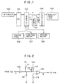
- a prior-art dot-matrix impact printer is shown in block diagram form in Fig. 1.
- Data from the information-processing apparatus are received via an interface circuit 100 and applied to a central processing unit (hereinafter referred to as a CPU) 101 which controls the operation of the printer.
- the CPU 101 communicates with other parts of the printer via an integrated I/O circuit (an I/O circuit formed of a large-scale integrated circuit) 102 which transfers signals from the printer's control panel 106 to the CPU 101 and transfers signals from the CPU 101 to a timer circuit 103, a drive circuit 104, a line-feed motor 107, and a spacing motor 108.
- the drive circuit 104 drives wires in a wire-dot print head 105, causing the printing of characters or other information.
- the control panel 106 comprises, for example, one or more pressure-sensitive membrane switches (not shown in the drawing) which, when pressed, generate electrical signals that are sent via the I/O circuit 102 to the CPU 101.
- the CPU 101 responds to these signals and to data received via the interface circuit 100 by controlling the timer circuit 103, the drive circuit 104, the line-feed motor 107, and the spacing motor 108 so that the desired information is printed by the wire-dot print head 105.
- the line-feed motor 107 moves the paper in the vertical direction and the spacing motor 108 moves the wire-dot print head 105 in the horizontal direction, enabling characters to be printed at different positions.
- Fig. 2 is a schematic diagram showing an example of part of the timer circuit 103 in Fig. 1, associated with one print wire. As illustrated, it comprises an open-collector NOT gate 109, a comparator 110, resistors 111, 112, and 113, a diode 114, and a capacitor 115. This circuit receives an input timing signal t1 from the I/O circuit 102 and generates an output timing signal t2 which it sends to the drive circuit 104 in Fig. 1.
- Fig. 3 is a timing chart illustrating the operation of the timer circuit in Fig. 2.
- the signal t1 received from the I/O circuit 102 which is a pulse signal with a High duration of T1 as shown in at (a) in Fig. 3, is inverted by the NOT gate 109, so when the signal t1 goes High, the output signal of the NOT gate 109 goes Low, allowing the capacitor 115 to discharge to ground level.
- the input of the NOT gate 109 goes Low again and its output returns to the High level (open state), causing the voltage Vh to charge the capacitor 115 through the resistor 111 with an RC time constant determined by the resistance (R111) of the resistor 111 and the capacitance (C115) of the capacitor 115.
- the output voltage of the NOT gate 109 rises as the capacitor 115 charges, as indicated in at (b) in Fig. 3. This rising voltage is received at the invert input terminal of the comparator 110.
- the output t2 of the comparator 110 thus remains at the High level for the time T2 until the charge in the capacitor 115 reaches the reference voltage level, as shown in at (c) in Fig. 3.
- the output signal t2 thus generated by the timer circuit 103 is referred to as the Overdrive signal.
- a part of the drive circuit 104 associated with one print wire is shown in Fig. 4. As illustrated, it comprises a buffer amplifier 116, an AND gate 117, NPN transistors 118 and 120, a PNP transistor 119, diodes 121 and 122, and resistors 124 and 125, which are connected to a head coil 123 for driving an associated print wire.
- the Overdrive signal t2 is received by the buffer amplifier 116, while the Enable signal t3 and Print signal t4 are received by the AND gate 117. The timing of these inputs is shown in Fig. 5.
- the Print signals select the wire to be driven. When the wire-dot print head 105 is at a given position on the paper, Print pulses are supplied only for the wires to be driven at that position.
- the NPN transistor 118 and the PNP transistor 119 both turn on.
- the drive circuit 104 receives both an Enable signal t3 and a Print signal t4
- the output of its AND gate 117 goes High, turning on the NPN transistor 120.
- a drive current I H is then permitted to flow from the power supply, which provides a voltage Vh, on a path marked R1 in Fig. 4 through the PNP transistor 119, the head coil 123, and the NPN transistor 120 to ground. This current flows during the interval d1 in at (d) in Fig. 5.
- the NPN transistor 118 and the PNP transistor 119 both turn off, but the electromotive force generated by the head coil 123 causes a residual current to flow on the path marked R2, circulating from the head coil 123 through the NPN transistor 120 and the diode 122, then back to the head coil 123.
- the current I H flowing through the head coil 123 therefore decreases gradually during the interval d2 in at (d) in Fig. 5.
- Fig. 6 shows a sectional view of the part of the wire-dot print head 105 for driving a print wire 131.
- the direction toward a printing paper PM in which the print wires are driven i.e., the upward direction as seen in Fig. 6 is referred to the forward direction or front.
- the head coil 123 is wound around a core 135 to form an electromagnet.
- the core 135 is secured to a base plate or rear yoke 137, at the perimeter of which is fastened a permanent magnet 138. Mounted on the permanent magnet 138 in sequence from bottom to top in Fig.
- FIGS. 6 are an upright support 139, a spacer 140, a plate spring 134, a front yoke 141, and a guide frame 130, the entire assembly being secured by an external clamp 142.
- An armature 132 is fastened to the inner free end of a radial part 134a of the plate spring 134, and the armature 132 is mounted on the plate spring 134.
- a print wire 131 is mounted to the armature 132. The tip of the print wire 131 extends through a central hole or a guide aperture in a guide frame 130 forward (upward in the drawing), i.e. toward the printing paper PM on the platen PL and out of the guide frame 130.
- a magnetic flux circuit is formed from the permanent magnet 138, through the core 135, the armature 132, and the front yoke 141 back to the permanent magnet 138.
- the flux generated by the permanent magnet 138 acts through the core 135 to attract the armature 132, thereby resiliently deforming the plate spring 134 as shown in Fig. 6, causing the print wire 131 to be kept retracting in the guide frame 130.
- the head coil 123 When the head coil 123 is energized, it creates a flux in the core 135 that acts counter to the flux generated by the permanent magnet 138, thus weakening the attractive power of the core 135, allowing the plate spring 134 to recover by the force of its own resiliency and drive the print wire 131 upward in Fig. 6. The end of the print wire 131 then presses an ink ribbon IR against the printing paper PM on the platen PL to print a dot.
- the print wires 131 in the wire-dot print head 105 are driven as selected by the Print signals as the wire-dot print head 105 moves back and forth and the paper moves in the feed-direction to print characters, symbols, and other information on the paper.
- the optimum energization time (drive time) of the head coil 123 varies depending on the printing conditions, including such factors as the time taken by the tip of the print wire 131 to reach the paper, the magnitude of the voltage Vh applied to the head coil 123, the number of print wires to be driven simultaneously, and the distance from the tip of the print wire to the paper (called the head gap).
- the pulse width T1 of the signal t1 is determined by the CPU 101 according to the number of wires to be driven simultaneously. As explained above, this time T1 is extended in the timer circuit 103 to the time T2, the amount of the extension being the time taken for the capacitor 115 to be charged through the resistor 111 by the voltage Vh, the extension thus being shorter when Vh is large and longer when Vh is small.
- the Overdrive signal t2 is thus corrected not only for the number of print wires driven simultaneously, but also for variations in the voltage Vh applied to the head coil 123.
- this system is capable of optimizing the drive time with respect to the two factors just mentioned, it does not enable the printing force (the force of impact of the print wires on the paper) to be varied freely in response to such factors as the thickness of the paper or the number of copies printed simultaneously.
- the printing force the force of impact of the print wires on the paper
- different types of paper and types of printing have different optimum impact forces. Thin paper, for example, does not require a large impact force, and a small impact force is preferable in that it reduces the noise of the printing process.
- Another problem is that if the impact force is adjusted to the optimum value for thin paper, when thick paper is used the impact force will be inadequate and the printing will be faint.
- a dot-matrix printer includes a wire-dot print head having print wires which print dots by impact on a printing medium, and a sensor for sensing the position of the print wires and generating signals indicating the position of the print wires.
- a parameter such as the power supply voltage or a reference voltage used for determining the timing of the termination of the drive current, determining a printing force with which each of the print wires impacts the printing medium is set.
- a control and driving circuit drives the print wire responsive to the signals from the sensors and the set parameter.
- Fig. 2 is a schematic diagram of the timer circuit in Fig. 1.
- Fig. 4 is a schematic diagram of the drive circuit in Fig. 1.
- Fig. 7 is a block diagram of a dot-matrix impact printer of an embodiment of the present invention.
- Fig. 8 is a sectional view of the print head of a dot-matrix impact printer according to the present invention.
- Fig. 9 is a plan view of the sensor card in the print head in Fig. 8.
- Fig. 10 is an oblique view illustrating the armature and sensor electrode in Fig. 8.
- Fig. 11 is a block diagram of an embodiment of the sensor circuit.
- Fig. 12 illustrates the principle of operation of the sensor circuit.
- Fig. 14 is a graph of the position vs. output voltage characteristic of the sensor circuit.
- Fig. 15 is a schematic diagram of the timing and drive circuits.
- Fig. 15A is a schematic diagram of the timing and drive circuits of the embodiment of Fig. 7A.
- Fig. 16 illustrates signal waveforms at various points in Fig. 15.
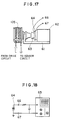
- Fig. 17 is a sectional view of a device for measuring impact force.
- Fig. 18 is a wiring diagram illustrating the connections of the device in Fig. 17.
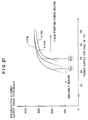
- Fig. 19 is a graph illustrating the printing voltage vs. impact force characteristic of a dot-matrix impact printer according to this invention.
- Fig. 20 is a graph illustrating the printing voltage vs. piezoelectric element output characteristic of a dot-matrix impact printer according to this invention.
- Fig. 21 is a graph illustrating the printing voltage vs. impact force characteristic of a prior-art dot-matrix impact printer.
- Fig. 7 is a block diagram of the novel dot-matrix impact printer. Blocks that correspond to blocks in Fig. 1 are indicated by the same reference numerals. (The same practice is followed in subsequent drawings.)
- the block labeled 50 is a power supply circuit which supplies necessary power to the wire-dot print head 105 via the drive circuits 104.
- the wire-dot print head 105 comprises, for each print wire, a sensor 51 which detects the displacement or position of the print wire.
- the output of the sensor 51 is provided to a sensor circuit 52 which generates a signal A corresponding to the position of the print wire.
- the signal A is sent to a timing circuit 53 which generates necessary timing signals, which it supplies to the drive circuit 104.
- the sensor 51, the sensor circuit 52, and the timing circuit 53 replace the timer circuit 103 in the prior art.
- the control panel 106 is provided with a printing force selection switch 106a which is manipulated for changing the power supply voltage Vh.
- the CPU 101 detects the manipulation of the selection switch 106a through the I/O circuit 102, and determines the selected power supply voltage Vh, and supplies a voltage designation signal H to the head drive power supply 50.
- the head drive power supply 50 is capable of selectively producing a voltage which can be varied stepwise. That is, the power supply 50 is capable of producing either a 35V voltage for strong printing force or a 17V voltage for weak printing force.
- Fig. 8 shows a sectional view of an embodiment of the wire-dot print head 105, which is generally cylindrical.
- the print head 105 has a generally disk-shaped cover 205 at the rear end (bottom as seen in Fig. 8) and a guide frame 130 at the front end (top as seen in Fig. 8).
- the guide frame 130 of this embodiment is formed of an electrically insulating material such as a plastic resin and has central guide apertures through which the print wires 131 protrude for impact on a print medium such as a print paper on a platen, not shown.
- the print wires 131 extend forward generally parallel with each other.
- "front” or “forward” refers to the direction toward which the print wires are moved for impact on the paper, i.e., upward as seen in Fig. 8.
- a generally disk-shaped base plate or rear yoke 137 of a magnetically permeable material an annular permanent magnet 138, an annular upright support 139, an annular spacer 140, a plate spring 134 having an annular part 134b and radial parts 134a extending from the annular part 134b radially inward, and a front yoke 141 having an annular part 141b and radial parts 141a extending from the annular part 141b radially inward so that they are positioned between adjacent radial parts 134a of the plate spring 134.
- the permanent magnet 138, the upright support 139, the spacer 140, the annular part 134b of the plate spring 134 and the annular part 141b of the front yoke 141 have generally the same outer and inner peripheries and form a cylindrical wall for the print head 105. All these components are held together by an external clamp 142.
- each radial part 134a of the plate spring 134 acts as a resilient support member for the associated armature 132. Because the radial part 134a act independently as individual springs, each of the radial parts 141a of the plate spring 141 is also called a plate spring.
- Each armature 132 is positioned between adjacent radial parts 141a of the front yoke 141.
- each print wire 131 is fixed to the inner end of the associated armature 132.
- Cores 135 are provided in association with the respective armatures 132. Each core 135 has its forward end adjacent to rear surface of the associated armature 132. The cores 135 are mounted on the rear yoke at their rear ends.
- Bobbins 16 are provided to surround the respective cores 135 and are also mounted on the rear yoke 137.
- Coils 123 are provided in association with the respective cores 135. Each coil 123 is wound on the bobbin 16 for the associated core 135, to form an electromagnet, which is electrically coupled via a coil terminal 17 to a printed circuit card 15 disposed beneath the rear yoke 137, between the rear yoke 137 and the cover 205.
- the printed circuit card 15 is fitted in a card-edge connector (not shown in the drawing) having terminals corresponding to the terminals 18.
- the printed circuit card 15 is provided with copper foil wiring, formed by patterning, for connecting respective coil terminals 17 and input terminals.
- the input terminals are electrically coupled to the drive circuit 104 in Fig. 7.
- the rear yoke 137, the cores 135, the armatures 132, the front yoke 141 the annular part 134b of the plate spring 134, the spacer 140, and the upright support 139 form a magnetic path for the magnetic flux from the permanent magnet 138. Because of this magnetic flux the armatures 132 are attracted to the cores 135.
- an electric current is made to flow through the coils 123 for generating a magnetic flux through the core 135 in a direction to cancel the magnetic flux through the core 135 from the permanent magnet 138.
- the associated armature 132 is attracted toward the associated core 135 to resiliently deform the associated resilient support member 134a.
- the associated armature 132 is released and moved forward by the action of the associated resilient support member 134a.
- a sensor card 11 in the form a printed circuit board is positioned in front of the front yoke 11, between the front yoke 141 and the guide frame 130.
- Sensor electrodes 13 are formed on the sensor card 11, and are created by patterning.
- the sensor electrodes 13 are in association with the respective armatures 132 and confront the front surfaces of the associated armatures 132 when the latter are moved forward, for printing.
- the armature 132 and the sensor electrode 13 form a pair of opposing plates with an air gap between them, thus acting as an air-gap capacitor with a static capacitance that depends on the width of the gap, hence on the position of the armature 132. It is this capacitor that is denoted as the capacitive sensor 51 in Fig. 7.
- the motion of the print wire 131 attached to the armature 132 can be detected by sensing the capacitance change of this capacitive sensor 51.
- the radial parts 141a of the front yoke 141 are on both sides of each armature 132 so that they effectively shield the sensor electrode 13 to avoid interference between adjacent sensor electrodes 13.
- Fig. 9 shows a plan view of the sensor card 11.
- the head is shown to have nine print wires 131, hence nine armatures 132 and nine sensor electrodes 13.
- An independent connecting line leads from each sensor electrode 13 to terminals 12.
- the terminals 12 are connected via the terminals of the card-edge connector to the sensor circuit 52 in Fig. 7.
- some connecting lines run on the same side of the sensor card 11 as the sensor electrodes 13, while others run on the opposite side and connected to the sensor electrodes 13 via through holes.
- the sensor electrodes 13, and the connecting lines as well as the rest of the sensor card 11 are coated with an insulating film, such as a photoresist applied over the entire surface of the sensor card. This coating insulates the electrodes and the connecting lines from the front yoke and provides protection against damages in case of collision during assembly or during operation of the print head.
- the armatures 132 are electrically coupled via the plate spring radial parts 134a to a common ground terminal, which is connected to the sensor circuit 52 as well as other circuits.
- the plate spring 134 is formed of a conductive material and joined at the circumference of the head.
- Fig. 10 is an oblique view showing how an armature 132 is mounted in relation to the front yoke 141, how it drives the print wire 131, its relation to the sensor electrode 13, and the connection of the sensor electrode 13 to the output terminal 12.
- the sensor card 15 is shown slightly separated from the front yoke 141, but when the wire-dot print head 105 is assembled, the sensor card 11 and the front surface of the front yoke 141 are actually in contact.
- the print wire 131 is attached to the end of the armature 132, which faces the sensor electrode 13. Since the sensor electrode 13 and the armature 132 are separated by a gap, they form a static capacitance, which acts as the sensor 51 in Fig.
- the part facing the sensor electrode 13 it is not necessary for the part facing the sensor electrode 13 to be the armature 132.
- Another component that is attached to the armature and moves together with the print wire 131 can be used instead.
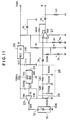
- Fig. 11 is a diagram of the sensor circuit 52 that receives the output from the sensor 51 and generates an output signal A indicating the position of the print wire 131.
- the sensor circuit 52 comprises a digital IC 23 such as the MSM74HCU04 manufactured by Oki Electric Industry Co. LTd., the output terminal of which is connected to the output terminal 12 on the sensor card 11.
- the sensor 51 is also connected to the sensor electrode 134, which functions as its common ground return.
- the sensor circuit 52 also comprises an oscillator 24 with a frequency f (Hz), a resistor 25 with a resistance Rs, a differentiator 26 comprising resistors and capacitors, an amplifier 27 having a gain Ga (such as the uPC258 manufactured by Nippon Denki Kabushiki Kaisha) and a regulator IC 28 (such as the 7805 manufactured by Nippon Denki Kabushiki Kaisha) that generates a regulated DC current. Additional resistors and capacitors are included in the circuit as shown in the drawing.
- the sensor circuit 52 in Fig. 11 can be depicted in a simplified form as shown in Fig. 12.
- the digital IC 23 is shown as comprising two MOS field-effect transistors 21 and 22 (hereinafter referred to as FETs) connected in series between the voltage V DD and the resistor 25.
- the digital IC 23 When the digital IC 23 receives a square-wave signal from the oscillator 24 as shown in at (a) in Fig. 13, the FETs 21 and 22 switch on and off alternately.
- the FET 21 When the FET 21 is on, the voltage V DD charges the capacitance of the sensor 51 through the FET 21.
- the FET 22 When the FET 22 is on, the charge stored in the sensor 51 discharges through the FET 22 and the resistor 25.
- the digital IC 23 therefore generates a current i c having the waveform indicated in at (b) in Fig. 13, obtained by differentiating the signal in at (a). Since the current i s flowing through the resistor 25 is a discharge current, it has a waveform like that shown in at (c) in Fig. 13.
- an AC amplifier is used as the amplifier 27, and its output contains, in addition to the component due to the capacitance of the sensor 51, a DC offset component caused by, for example, distributed capacitance effects.
- the offset component is removed to leave the component representing the position of the print wire 131.
- the capacitance C x of the sensor 51 is substantially inversely-proportional to the distance between the armature 132 and the sensor electrode 13.
- the output voltage V 0 of the sensor circuit 52 therefore varies with respect to the position of the print wire 131 as shown in Fig. 14.
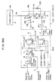
- Fig. 15 shows a detailed view of the timing circuit 53 and the drive circuit 104.
- the timing circuit 53 comprises a differentiator 30 (a high-pass filter) that differentiates the position signal (the voltage V 0 ) output by the sensor circuit 52, a comparator 32 that compares the output of the differentiator 30 with a reference voltage obtained from a variable resistor 31, NOT gates 33 and 34 which receive input signals and generate their inverted output, and delay flip-flop circuits 35 and 36 (D flip-flops) which receive signals with a certain High level (of +5V) at their data (D) terminals.
- the drive circuit 104 comprises, in addition to the components shown in Fig. 4, resistors 71 and 72, but is basically similar to the circuit in Fig. 4.
- the NPN transistor 118 and the PNP transistor 119 both switch on.
- the AND gate 117 receives at one of its inputs a Print signal t4 from the integrated I/O circuit 102, so when the output signal (E) from the D flip-flop 36 (which corresponds to the Enable signal in the prior art) goes High, the AND gate 117 generates a High output signal that switches on the NPN transistor 120.
- a head current I H flows through the PNP transistor 119, the head coil 123, and the NPN transistor 120 to ground, as indicated in at (g) in Fig. 16.
- the position signal A generated by the sensor circuit 52 is supplied to the differentiator 30, which differentiates it.
- the output B of the differentiator 30 (the velocity signal) gradually increases in the positive direction as shown in at (c) in Fig. 16, reaches a positive peak at the instant of impact, jumps down to a negative peak when backward motion begins, then gradually recovers to zero.
- the reference voltage is adjusted to detect onset of forward motion of the print wire 131.
- the output signal B of the differentiator 30 thus increases during the interval from when the print wire 131 starts to move forward until it impacts the paper and starts to move backward. It is during this interval that the output C of the differentiator 30 is High, as indicated in at (d) in Fig. 16.
- the print wire 131 begins moving forward, it continues to move forward under the resilient force of the sensor electrode 134, so it is unnecessary to supply further current to the head coil 123. For this reason the Clock (CK) terminal of the D flip-flop 35 receives the output C of the differentiator 30, the leading edge of which causes the D flip-flop 35 to invert, as shown in at (e) in Fig. 16, switching the PNP transistor 119 off.
- a residual current (the current R2 described in the prior art) now circulates through the diode 122, the head coil 123, and the NPN transistor 120.
- the head coil 123 no longer requires the residual current, so the output of the comparator 32 is inverted by the NOT gate 33 and supplied to the Clock input terminal of the D flip-flop 36.
- the output E of the D flip-flop 36 thus inverts at the moment of impact of the print wire 131 (on the trailing edge of the output of the comparator 32), as shown in at (f) in Fig. 16, turning off the NPN transistor 120.
- the residual current flow is then quickly absorbed on the path from ground to the diode 122, the head coil 123, and the diode 121, to the power supply circuit 50, as indicated in at (g) in Fig. 16.
- the drive time of the print wire 131 is thus controlled in a closed-loop fashion according to the actual motion of the print wire, enabling sufficient energy to be supplied to the wire-dot print head 105 regardless of variations in the paper thickness and other factors.
- the printing process can thus be carried out efficiently with optimal timing.
- printing force can be varied, with a high reproducibility, by variation of the power supply voltage Vh as will be later described in further detail.
- Fig. 7A shows a second embodiment of the invention.
- the CPU detects the manipulation of the control panel 106 and determines the selected reference voltage, and supplies a D/A converter 204, through the I/O circuit 102, with a digital signal Ga designating the reference voltage G, and the D/A converter 204 produces an analog voltage reference signal G and sends it to a timing circuit 53A whose details are shown in Fig. 15A, and which is similar to, but a little different from the timing circuit 53 shown in Fig. 15. That is, as illustrated in Fig. 15A, the reference voltage G to the comparator 32 is supplied from the D/A converter 204.
- the power supply circuit 50 of this embodiment can be of such a construction as to produce a fixed voltage of say 35V.
- Changing the reference voltage G causes changing the timing T1 (Fig. 16) at which the transistor 119 (Fig. 15A) is turned off. This has the effect of varying the printing force.
- the change in printing force resulting from changes in the voltage Vh applied to the head coil 123 in a wire-dot print head 105 of the above structure and from changes in the reference voltage G was measured with the measurement apparatus shown in Fig. 17, comprising a test mount 61 with a block 62 fixed at one end, a piezoelectric element 64 attached to the block 62, and a super-hard metal alloy target 63 mounted on the piezoelectric element 64.
- the wire-dot print head 105 was mounted at the other end of the test mount 61 in such a position that its print wires would impact the super-hard metal alloy target 63.
- the output terminals 66 and 67 of the piezoelectric element 64 were connected to an oscilloscope through a low-pass filter comprising a resistor and a capacitor as shown in Fig. 18, and the peak-to-peak output values (indicating printing force) of the piezoelectric element 64 were observed.
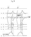
- Fig. 19 shows the results.
- Fig. 21 shows the printing force vs. applied voltage Vh characteristic of a prior-art wire-dot print head as measured in the same way.
- printing becomes unstable below approximately 21V (to the left of the line Rc in Fig. 20), while a substantially constant printing force is obtained above approximately 25V (to the right of the line Rd in Fig. 20).
- the intermediate region (between the lines Rc and Rd) in which the printing force can be adjusted by altering the voltage Vh is comparatively narrow, and the rate of change of the printing force in this interval is correspondingly steep.
- printing conditions such as the number of dots to be printed simultaneously.
- the number of wires (pins) to be driven simultaneously can cause variation in the printing force in the region in which the variation of the printing force is possible.
- This is in contrast to the situation in the invention in which the printing force is not substantially varied with the number of pins simultaneously driven, and differences between individual heads, difference in the head gap, and other printing conditions.
- it is therefore difficult to adjust or modify the printing force in a reliable manner in this interval.
- the reason is that the driving time of the print wires is determined without relation to the state of motion of the print wires. A consequence of this is that it is extremely difficult to reduce the energy supplied to the wire-dot print head and still maintain the required printing force, due to manufacturing variations in the paper and the wire-dot print head.
- the power supply voltage Vh or the reference voltage G is used as a parameter determining the printing force. Any other parameter determining the printing force can alternatively be used and altered for changing the printing force.
- the parameter determining the printing force is changed responsive to manipulation of the control panel by the operator.
- the voltage generated by the sensor circuit 52 can be altered automatically in response to the output of a gap adjustment lever or paper thickness sensor (not shown in the drawings).
- the invention was described in relation to a spring-release wire-dot print head, but it can also be applied to other types of heads, such as the clapper type and the piezoelectric type.
- the invention has the combination of the feature that print wires are driven according to the output of sensors that sense their position, and that a parameter determining the printing force is changed, the examples of the parameter being the driving voltage and the reference voltage. Because of the combined features, the printing force can be adjusted in a stable fashion, i.e., with a high reproducibility. In other words, the optimum energy can always be supplied, regardless of variations in factors such as paper thickness, so printing of constant quality can be obtained in an efficient manner, with minimal noise. This enables such new dot-matrix impact printing features as halftone printing with variable dot size and darkness.
Landscapes
- Dot-Matrix Printers And Others (AREA)
Claims (12)
- Punktmatrix-Anschlagdrucker, der folgendes umfaßt:
einen Nadel-Punkt-Druckkopf (105) mit einem oder mehreren Drucknadeln (131), die Punkte durch Anschlagen auf ein Druckmedium (PM) drucken;
eine Meßeinrichtung (51, 52) zum Messen der Position der Drucknadeln und zum Erzeugen von Signalen, die die Position der Drucknadeln anzeigen;
eine Einrichtung (106a) zum Einstellen eines Parameters, der eine Druckkraft bestimmt, mit der jede der Drucknadeln auf das Druckmedium anschlägt;
eine Steuer- und Antriebseinrichtung (53 oder 53A, 101, 104), die auf die Signale von der Meßeinrichtung (51, 52) und der Parameter-Einstelleinrichtung (106a) anspricht, um die Drucknadeln mit einer durch die Signale bestimmten Zeiteinstellung anzutreiben; und
eine Spannungsversorgung (50) zum Erregen des Druckkopfs;
dadurch gekennzeichnet, daß
die Spannungsversorgung (50) eine veränderbare Spannung erzeugen kann und der Parameter die Spannung der Spannungsversorgung ist und
die Spannung der Spannungsversorgung als Reaktion auf die Einstelleinrichtung (106a) verändert wird. - Punktmatrix-Anschlagdrucker, der folgendes umfaßt:
einen Nadel-Punkt-Druckkopf (105) mit einem oder mehreren Drucknadeln (131), die Punkte durch Anschlagen auf ein Druckmedium (PM) drucken;
Meßeinrichtung (51, 52) zum Messen der Position der Drucknadeln und zum Erzeugen von Signalen, die die Position der Drucknadeln anzeigen;
eine Einrichtung (106a) zum Einstellen eines Parameters, der eine Druckkraft bestimmt, mit der jede der Drucknadeln auf das Druckmedium anschlägt; und
eine Steuer- und Antriebseinrichtung (53 oder 53A, 101, 104), die auf die Signale von der Meßeinrichtung (51, 52) und der Parameter-Einstelleinrichtung (106a) anspricht, um die Drucknadeln mit einer durch die Signale bestimmten Zeiteinstellung anzutreiben;
dadurch gekennzeichnet, daß
die Steuer- und Antriebseinrichtung weiterhin folgendes umfaßt:
eine Einrichtung (30A), die auf die Meßeinrichtung anspricht, um ein Signal zu erzeugen, das die Geschwindigkeit der Drucknadeln anzeigt; und
einen Komparator (32) zum Vergleichen des Geschwindigkeitsignals mit einem Referenzsignal (G);
und daß der Parameter das Referenzsignal (G) ist und
das Referenzsignal als Reaktion auf die Einstelleinrichtung (106a) verändert wird. - Punktmatrix-Anschlagdrucker nach Anspruch 1 oder 2, bei dem die Meßeinrichtung (51, 52) folgendes umfaßt:
eine Vielzahl von kapazitiven Sensoren (51), die den entsprechenden Drucknadeln (131) zugeordnet sind, wobei die Kapazität jedes kapazitiven Sensors entsprechend der Position der zugeordneten Drucknadel variiert; und
eine Kapazitäts-Erkennungsschaltung (52), die mit den kapazitiven Sensoren (51) verbunden ist, um elektrische Signale zu erzeugen, die die Kapazitäten der kapazitiven Sensoren anzeigen. - Punktmatrix-Anschlagdrucker nach Anspruch 3, bei dem jeder der kapazitiven Sensoren (51) für jede Drucknadel folgendes umfaßt:
eine feststehende Elektrode (13), die an einem feststehenden Teil des Druckkopfes befestigt ist; und
eine bewegliche Elektrode (132), die mit der Drucknadel beweglich ist, so daß die Entfernung zwischen der feststehenden Elektrode und der beweglichen Elektrode mit der Bewegung der Drucknadel variiert;
wodurch die Kapazität zwischen der feststehenden Elektrode und der beweglichen Elektrode mit der Bewegung der Drucknadel variiert. - Punktmatrix-Anschlagdrucker nach Anspruch 4, bei dem die bewegliche Elektrode von einem Magnetanker (132) gebildet ist, an dem die Drucknadel befestigt ist.
- Punktmatrix-Anschlagdrucker nach Anspruch 5, bei dem
sich die Drucknadeln (131) allgemein parallel zueinander nach vorne erstrecken, und
die Magnetanker (132) den entsprechenden Drucknadeln zugeordnet sind, wobei ein hinters Ende jeder Drucknadel (131) fest mit dem zugeordneten Magnetanker verbunden ist, und
wobei der Druckkopf weiterhin folgendes umfaßt:
Spulenkerne (135), die den jeweiligen Magnetankern zugeordnet sind, wobei das vordere Ende jedes Spulenkerns an die hintere Oberfläche des zugeordneten Magnetankers angrenzt,
Spulen (123), die den entsprechenden Spulenkernen zugeordnet sind, wobei jede Spule auf den zugeordneten Spulenkern gewickelt ist,
wobei jede der Spulen (123) und der zugeordnete Spulenkern (135) einen Elektromagneten bilden,
eine zylindrische Wand (138, 139, 140, 134b, 141b), die die Magnetanker, die Spulenkerne und die Spulen umgibt,
einen ringförmigen Permanentmagneten (138), der einen Teil der zylindrischen Wand bildet,
federnde Trageglieder (134), die den entsprechenden Magnetankern zugeordnet sind, wobei jedes federnde Trageglied ein erstes Ende besitzt, das fest mit der zylindrischen Wand verbunden ist und ein zweites Ende, das fest mit dem zugeordneten Magnetanker verbunden ist,
ein vorderes Joch (141), das Vorsprünge besitzt, die sich von der zylindrischen Wand radial einwärts erstrecken, wobei jeder Vorsprung auf einer Seite einer der Magnetanker positioniert ist,
eine Magnetwegeinrichtung (137, 135, 132, 141, 134b, 140, 139), die es einem Magnetfluß ermöglicht, von dem Permanentmagneten durch den Spulenkern, den Magnetanker und das vordere Joch hindurchzufließen,
wobei die Steuer- und Antriebseinrichtung bewirkt, daß ein elektrischer Strom durch die Spulen fließt, um einen Magnetfluß durch die Spulenkerne in eine Richtung zu erzeugen, um den Magnetfluß von dem Permanentmagneten durch den Spulenkern aufzuheben,
der zugeordnete Magnetanker zum zugeordneten Spulenkern anzogen wird, um das zugeordnete federnde Trageglied federnd zu verformen, wenn keine der Spulen erregt ist, und
der zugeordnete Magnetanker losgelassen wird und sich unter der Wirkung des zugeordneten federnden Trageglieds vorwärts bewegt, wenn jede der Spulen erregt ist. - Punktmatrix-Anschlagdrucker nach Anspruch 6, der weiterhin ein im wesentlichen scheibenförmiges hinteres Joch (137) umfaßt, das den Permanentmagneten (138) und die Magnetanker (135) verbindet; und
eine Sensorkarte (11), die vor den Magnetankern (132) positioniert ist, und die eine rückseitige Oberfläche besitzt, auf der die feststehenden Elektroden (13) so ausgebildet sind, daß sie den Magnetankern gegenüberstehen. - Punktmatrix-Anschlagdrucker nach Anspruch 1 oder 2, bei dem
der Druckkopf eine Vielzahl von Elektromagneten (123, 135), die den entsprechenden Drucknadeln zugeordnet sind, umfaßt, und der so aufgebaut ist, daß jede Drucknadel zum Druckmedium bewegt wird, wenn der zugeordnete Elektromagnet erregt ist; und
die Steuer- und Antriebseinrichtung folgendes umfaßt:
eine Steuerschaltung (101) zum Erzeugen eines Drucksignals;
eine Zeiteinstellungsschaltung (53 oder 53A) zum Erzeugen eines Einsatz-Erkennungssignals, das den Einsatz der Bewegung der Drucknadeln anzeigt und eines Anschlag-Erkennungssignals, das den Augenblick ihres Anschlag auf das Druckmedium anzeigt; und
eine Antriebsschaltung (104), die folgendes umfaßt:
eine erste Stromwegeinrichtung (R1) zum Verbinden des Elektromagneten über ein Paar Spannungsversorgungsanschlüsse, um einen Stromfluß von der Spannungsversorgung (50) zu dem Elektromagneten zuzulassen;
eine zweite Stromwegeinrichtung (R2) zum Verbinden einer Widerstandseinrichtung über den Elektromagneten, um zu gestatten, daß elektrischer Strom aufgrund irgendeiner Quellenspannung, die in den Elektromagneten induziert wurde, durch die Widerstandseinrichtung fließt;
eine dritte Stromwegeinrichtung (R3) zum Verbinden des Elektromagneten mit der Spannungsversorgung, um zu gestatten, daß elektrischer Strom aufgrund einer Quellenspannung, die in den Elektromagneten induziert wurde, zu der Spannungsversorgung fließt;
eine Stromweg-Steuereinrichtung (116, 118, 125, 117, 124), die bewirkt, daß ein elektrischer Strom durch die erste Stromwegeinrichtung fließt, um den Elektromagneten bei Empfang des Drucksignals zu erregen, und die auf die Zeiteinstellungsschaltung anspricht, um bei Empfang des Einsatz-Erkennungssignals den Stromfluß durch die erste Stromwegeinrichtung zu beenden und den Stromfluß durch die zweite Stromwegeinrichtung zu initiieren und bei Empfang des Anschlag-Erkennungssignals den Stromfluß durch die zweite Stromwegeinrichtung zu beenden und den Stromfluß durch die dritte Stromwegeinrichtung zu initiieren. - Punktmatrix-Anschlagdrucker nach Anspruch 8, bei dem die Drucknadel dadurch zurückgezogen wird, daß sie von einem Permanentmagneten (138) angezogen wird, wenn der zugeordnete Elektromagnet (123, 135) nicht mehr erregt ist.
- Punktmatrix-Anschlagdrucker nach Anspruch 8, bei dem die Stromweg-Steuereinrichtung (116, 118, 125, 117, 124) eine festgesetzte Zeit, nachdem das Einsatz-Erkennungssignals erzeugt wurde, den Stromfluß durch die erste Stromwegeinrichtung beendet und den Stromfluß durch die zweite Stromwegeinrichtung initiiert.
- Punktmatrix-Anschlagdrucker nach Anspruch 1, bei dem die Spannungsversorgung (50) entsprechend der eingestellten Druckkraft entweder eine erste Spannung oder eine zweite Spannung, die niedriger ist als die erste Spannung, erzeugen kann.
- Punktmatrix-Anschlagdrucker nach Anspruch 2, bei dem die Einrichtung (106a) zum Einstellung des Parameters, der die Druckkratt bestimmt, einen Schalter umfaßt.
Applications Claiming Priority (4)
| Application Number | Priority Date | Filing Date | Title |
|---|---|---|---|
| JP73634/88 | 1988-03-28 | ||
| JP63073634A JP2553137B2 (ja) | 1988-03-28 | 1988-03-28 | ワイヤドットインパクトプリンタ |
| JP130990/88 | 1988-05-27 | ||
| JP13099088A JP2505532B2 (ja) | 1988-05-27 | 1988-05-27 | ワイヤドットインパクトプリンタ装置 |
Publications (3)
| Publication Number | Publication Date |
|---|---|
| EP0335257A2 EP0335257A2 (de) | 1989-10-04 |
| EP0335257A3 EP0335257A3 (en) | 1990-08-16 |
| EP0335257B1 true EP0335257B1 (de) | 1994-07-27 |
Family
ID=26414774
Family Applications (1)
| Application Number | Title | Priority Date | Filing Date |
|---|---|---|---|
| EP89105214A Expired - Lifetime EP0335257B1 (de) | 1988-03-28 | 1989-03-23 | Punktmatrix-Anschlagdrucker |
Country Status (3)
| Country | Link |
|---|---|
| US (1) | US5039238A (de) |
| EP (1) | EP0335257B1 (de) |
| DE (1) | DE68916991D1 (de) |
Families Citing this family (9)
| Publication number | Priority date | Publication date | Assignee | Title |
|---|---|---|---|---|
| US5257674A (en) * | 1988-11-14 | 1993-11-02 | Yamaha Hatsudoki Kabushiki Kaisha | Engine construction for vehicle |
| DE58908638D1 (de) * | 1989-09-18 | 1994-12-15 | Mannesmann Ag | Matrixnadeldruckkopf. |
| US5190383A (en) * | 1991-06-26 | 1993-03-02 | Brother Kogyo Kabushiki Kaisha | Dot printing apparatus |
| JPH0538847A (ja) * | 1991-08-07 | 1993-02-19 | Tokyo Electric Co Ltd | ドツトプリンタヘツドの出力制御装置 |
| JPH0584934A (ja) * | 1991-09-30 | 1993-04-06 | Nec Niigata Ltd | プリンタ |
| JP2567506Y2 (ja) * | 1992-02-13 | 1998-04-02 | 東北沖電気株式会社 | ワイヤドット印字ヘッド |
| JP2937712B2 (ja) * | 1993-10-22 | 1999-08-23 | 沖電気工業株式会社 | ワイヤドットヘッドのワイヤ動作検出装置 |
| US6027265A (en) * | 1997-10-14 | 2000-02-22 | Powis Parker, Inc. | Printer having improved print head mechanism and method |
| JP2002019165A (ja) * | 2000-06-26 | 2002-01-23 | Internatl Business Mach Corp <Ibm> | プリンタ、伝票プリンタ、プリンタの制御方法、印字コントローラ |
Family Cites Families (9)
| Publication number | Priority date | Publication date | Assignee | Title |
|---|---|---|---|---|
| NL177294C (nl) * | 1977-11-03 | 1985-09-02 | Philips Nv | Drukker, voorzien van een slaginrichting met opnemer. |
| JPS5582684A (en) * | 1978-12-19 | 1980-06-21 | Ricoh Co Ltd | Mark printing circuit |
| US4347786A (en) * | 1979-10-01 | 1982-09-07 | International Business Machines Corporation | Impact printer hammer flight time and velocity sensing means |
| US4348119A (en) * | 1980-11-06 | 1982-09-07 | General Electric Company | Bounce control system for moving coil printing element |
| DE3112742A1 (de) * | 1981-03-31 | 1982-10-07 | Olympia Werke Ag, 2940 Wilhelmshaven | Anordnung zur steuerung der staerke des typenabschlages in schreib- oder aehnlichen maschinen |
| JPS592864A (ja) * | 1982-06-30 | 1984-01-09 | Hitachi Ltd | インパクト型プリンタ |
| JPS59120478A (ja) * | 1982-12-27 | 1984-07-12 | Canon Inc | 出力制御方法 |
| JPS59150755A (ja) * | 1983-02-18 | 1984-08-29 | Oki Electric Ind Co Ltd | ドツトインパクト印字ヘツド |
| JPH0798398B2 (ja) * | 1985-05-24 | 1995-10-25 | セイコーエプソン株式会社 | 印刷装置 |
-
1989
- 1989-03-22 US US07/327,480 patent/US5039238A/en not_active Expired - Fee Related
- 1989-03-23 EP EP89105214A patent/EP0335257B1/de not_active Expired - Lifetime
- 1989-03-23 DE DE68916991T patent/DE68916991D1/de not_active Expired - Lifetime
Also Published As
| Publication number | Publication date |
|---|---|
| DE68916991D1 (de) | 1994-09-01 |
| EP0335257A3 (en) | 1990-08-16 |
| EP0335257A2 (de) | 1989-10-04 |
| US5039238A (en) | 1991-08-13 |
Similar Documents
| Publication | Publication Date | Title |
|---|---|---|
| EP0335257B1 (de) | Punktmatrix-Anschlagdrucker | |
| US4514737A (en) | Printing head driving apparatus | |
| EP0348516B1 (de) | Nadelpunktdrucker | |
| EP0305871B1 (de) | Apparat zum Betreiben eines Nadeldruckkopfes | |
| US5518323A (en) | Method of adjusting a head gap for a wire dot impact printer | |
| US5074686A (en) | Automatic gap adjustment apparatus for printing head | |
| KR900007521B1 (ko) | 잉크 도트 프린터 | |
| US5518327A (en) | Wire motion detecting apparatus for wire dot head and wire dot impact printer apparatus therewith | |
| US5071268A (en) | Wire-dot print head driving apparatus having sensing coils | |
| US4812062A (en) | Print hammer with flux detection for print pressure control | |
| EP0272287B1 (de) | Anschlagstärkesteuerung für drucker | |
| EP0395763A1 (de) | Druckvorrichtung mit punktanschlag | |
| GB2292545A (en) | A method of adjusting the head gap of a wire dot impact printer | |
| JP2553137B2 (ja) | ワイヤドットインパクトプリンタ | |
| JP2746787B2 (ja) | ワイヤドット印字ヘッドの制御装置 | |
| JPS626995B2 (de) | ||
| JP2869225B2 (ja) | ワイヤドットプリンタ | |
| JPS6315152B2 (de) | ||
| JPS62238759A (ja) | ドツトインパクト式プリンタ | |
| JPH0313353A (ja) | インパクトドットヘッド | |
| JPS6174857A (ja) | 印字ヘツドにおけるワイヤのインパクト検知方式 | |
| JPH05112018A (ja) | インパクトプリンタのヘツド通電方法 | |
| JPH0564598B2 (de) | ||
| JPS6360763A (ja) | 圧電型印字ヘツド駆動回路 | |
| JPH0577457A (ja) | インパクトプリンタ |
Legal Events
| Date | Code | Title | Description |
|---|---|---|---|
| PUAI | Public reference made under article 153(3) epc to a published international application that has entered the european phase |
Free format text: ORIGINAL CODE: 0009012 |
|
| AK | Designated contracting states |
Kind code of ref document: A2 Designated state(s): DE FR GB |
|
| PUAL | Search report despatched |
Free format text: ORIGINAL CODE: 0009013 |
|
| AK | Designated contracting states |
Kind code of ref document: A3 Designated state(s): DE FR GB |
|
| 17P | Request for examination filed |
Effective date: 19901206 |
|
| 17Q | First examination report despatched |
Effective date: 19920707 |
|
| GRAA | (expected) grant |
Free format text: ORIGINAL CODE: 0009210 |
|
| AK | Designated contracting states |
Kind code of ref document: B1 Designated state(s): DE FR GB |
|
| PG25 | Lapsed in a contracting state [announced via postgrant information from national office to epo] |
Ref country code: FR Effective date: 19940727 |
|
| REF | Corresponds to: |
Ref document number: 68916991 Country of ref document: DE Date of ref document: 19940901 |
|
| PG25 | Lapsed in a contracting state [announced via postgrant information from national office to epo] |
Ref country code: DE Effective date: 19941028 |
|
| EN | Fr: translation not filed | ||
| PLBE | No opposition filed within time limit |
Free format text: ORIGINAL CODE: 0009261 |
|
| STAA | Information on the status of an ep patent application or granted ep patent |
Free format text: STATUS: NO OPPOSITION FILED WITHIN TIME LIMIT |
|
| 26N | No opposition filed | ||
| PGFP | Annual fee paid to national office [announced via postgrant information from national office to epo] |
Ref country code: GB Payment date: 19980316 Year of fee payment: 10 |
|
| PG25 | Lapsed in a contracting state [announced via postgrant information from national office to epo] |
Ref country code: GB Free format text: LAPSE BECAUSE OF NON-PAYMENT OF DUE FEES Effective date: 19990323 |
|
| GBPC | Gb: european patent ceased through non-payment of renewal fee |
Effective date: 19990323 |