EP0336352A2 - Micro-élément de construction - Google Patents
Micro-élément de construction Download PDFInfo
- Publication number
- EP0336352A2 EP0336352A2 EP89105850A EP89105850A EP0336352A2 EP 0336352 A2 EP0336352 A2 EP 0336352A2 EP 89105850 A EP89105850 A EP 89105850A EP 89105850 A EP89105850 A EP 89105850A EP 0336352 A2 EP0336352 A2 EP 0336352A2
- Authority
- EP
- European Patent Office
- Prior art keywords
- micro
- components
- openings
- recesses
- component according
- Prior art date
- Legal status (The legal status is an assumption and is not a legal conclusion. Google has not performed a legal analysis and makes no representation as to the accuracy of the status listed.)
- Withdrawn
Links
Images

Classifications
-
- B—PERFORMING OPERATIONS; TRANSPORTING
- B07—SEPARATING SOLIDS FROM SOLIDS; SORTING
- B07B—SEPARATING SOLIDS FROM SOLIDS BY SIEVING, SCREENING, SIFTING OR BY USING GAS CURRENTS; SEPARATING BY OTHER DRY METHODS APPLICABLE TO BULK MATERIAL, e.g. LOOSE ARTICLES FIT TO BE HANDLED LIKE BULK MATERIAL
- B07B1/00—Sieving, screening, sifting, or sorting solid materials using networks, gratings, grids, or the like
- B07B1/46—Constructional details of screens in general; Cleaning or heating of screens
- B07B1/4609—Constructional details of screens in general; Cleaning or heating of screens constructional details of screening surfaces or meshes
- B07B1/4618—Manufacturing of screening surfaces
-
- B—PERFORMING OPERATIONS; TRANSPORTING
- B01—PHYSICAL OR CHEMICAL PROCESSES OR APPARATUS IN GENERAL
- B01D—SEPARATION
- B01D29/00—Filters with filtering elements stationary during filtration, e.g. pressure or suction filters, not covered by groups B01D24/00 - B01D27/00; Filtering elements therefor
- B01D29/01—Filters with filtering elements stationary during filtration, e.g. pressure or suction filters, not covered by groups B01D24/00 - B01D27/00; Filtering elements therefor with flat filtering elements
- B01D29/012—Making filtering elements
-
- B—PERFORMING OPERATIONS; TRANSPORTING
- B01—PHYSICAL OR CHEMICAL PROCESSES OR APPARATUS IN GENERAL
- B01D—SEPARATION
- B01D29/00—Filters with filtering elements stationary during filtration, e.g. pressure or suction filters, not covered by groups B01D24/00 - B01D27/00; Filtering elements therefor
- B01D29/01—Filters with filtering elements stationary during filtration, e.g. pressure or suction filters, not covered by groups B01D24/00 - B01D27/00; Filtering elements therefor with flat filtering elements
- B01D29/03—Filters with filtering elements stationary during filtration, e.g. pressure or suction filters, not covered by groups B01D24/00 - B01D27/00; Filtering elements therefor with flat filtering elements self-supporting
-
- B—PERFORMING OPERATIONS; TRANSPORTING
- B23—MACHINE TOOLS; METAL-WORKING NOT OTHERWISE PROVIDED FOR
- B23P—METAL-WORKING NOT OTHERWISE PROVIDED FOR; COMBINED OPERATIONS; UNIVERSAL MACHINE TOOLS
- B23P13/00—Making metal objects by operations essentially involving machining but not covered by a single other subclass
Definitions
- the invention relates to micro-components, such as micro-sieves, micro-grids, micro-sensors or other micro-measuring or micro-test or micro-carriers or other components with micro-openings or recesses and the largest possible free surface.
- Micro devices are used for many purposes.
- the object of the invention is to provide a microcomponent which can be produced in a simple and rational manner, is suitable for a large number of starting materials and creates a wide range of uses for the components.
- a micro component has a body 1, in particular substrate body in the form of a film or plate, e.g. from one of the above Materials or composites hereby.
- the lattice structure 2 e.g. as shown in the drawing and preferably machined in the surface outlet area, from both sides of the body 1 with the largest surfaces - in the drawing from above and from below. This also creates a structure for these surfaces.
- With 3 are incorporated grooves / channels, with 4 and 5 openings of angular or round cross-section, with 6 a support layer, with 7 gaps and with 8 and 9 the height or thickness that remains.
- ⁇ and ⁇ relate to angles (see Fig. 1).
- the fabrication of the screens and grids is possible in a variety of materials.
- the processing of the structures by turning, milling, broaching or grinding with diamond or CBN tools depends on the respective material selection.
- the starting material is positioned on a machine selected according to the manufacturing process by means of a vacuum clamping device and held by vacuum.
- the machining process, turning, milling broaching or grinding determines the shape of the starting material (foils or plates) and at the same time the use of suitable vacuum clamping devices, e.g. in cylinder or plate design.
- the tools for the cutting process are preferably microdiamond form cutting, polycrystalline diamond micro cutting, CBN tools and diamond or CBN grinding wheels.
- the surface of the film / plate held on the clamping device is structured by a cutting tool or a grinding wheel.
- the foil / plate processed on one side is supported by a layer. This prevents the formation of burrs in the desired penetration in the structural area. In the case of grid designs for sensors or electrical conductor tracks, this layer can be used as a support and / or insulator.
- the film / plate structured and coated on one side is applied with the machined surface to the tensioning / holding device.
- the channels / grooves are machined transversely to the structures on the underside.
- the angular course of the structures on the top and bottom is between 30 ° - 90 °.
- the distances and the depth of the incorporated structures depend on the desired shape and size of the openings.
- the size of the openings depends in particular on the width and the overlap of the incorporated structures.
- the shape of the openings results from the selected structural geometry (cf. FIG. 1).
- Micro sieves, lattice structures or sensors can be produced by machining the surfaces on both sides (two-dimensional).
- the incorporated structures overlap in depth.
- the structures on the surfaces run at an angle of 30 ° - 90 ° to each other.
- the shape of the structures is preferably rectangular, semicircular or acute-angled with a radius.
- the depth of the overlap and the shape at the bottom of the grooves determine the geometry and size of the openings (three-dimensional).
- the shape of the openings is preferably square, rectangular, round or oval.
- the strength of the sieves can be increased by support bars, which are arranged on both surfaces according to the structure.
- the structure is provided with a support layer.
- Layer thickness ⁇ 0.03. This can serve as the desired insulation between the structures.
- - Preferred materials Al alloy, Cu alloy, Ti alloy, high-strength, acid-resistant steels, Ni alloy, molybdenum, noble metals such as gold, silver, platinum as well as ceramics and semiconductors.
- - Preferred dimensions thickness of the sieves / grids 0.02 - 0.2 mm size of the openings diameter> 0.005 mm spacing of the openings> 0.01 mm surface area ⁇ Ra 0.1
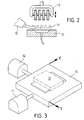
- Combination (change) tools 13 of the above type and method and their preferably automatic control according to the program with a microprocessor / robot are known and can be used here (CIM), e.g. with robot gripping arm 15 for holding the workpiece 14 (see FIG. 2).
- CCM Combination (change) tools 13 of the above type and method and their preferably automatic control according to the program with a microprocessor / robot
- a magnetic clamping table or the like can be used instead of a vacuum clamping device.
- x-y table 10 can be used.
- a piezoelectric motor (inchworm motor) or linear motor (PZT pusher) can serve as the drive for such a clamping table.
- Such drives 11, 12 are known per se. They work almost without play and can be seen in Fig. 3.
- semiconductors such as Si, GaAs, ceramics such as AlN, TiN, Al2O3, TiC, oa borides, carbides, oxides, nitrides, silicides; Glasses, in particular high-melting types such as quartz glass (SiO2) or composites with them, such as metal ceramics, glass ceramics, glass metals and others, including multilayer composites, are used, depending on the application, for example as a micro sieve or mesh or mesh for apparatuses or devices in physical / chemical engineering, in particular measuring and analysis technology preferably made of metal, ceramic, glass, for example for micro sensors, preferably made of semiconductors (FETs), metal, metal ceramics (cermet) and eg as a carrier for biological cells and treatment in research and for example as a catalyst carrier.
- FETs semiconductors
- metal, metal ceramics (cermet) eg as a carrier for biological cells and treatment in research and for example as a catalyst carrier.
- removable films preferably made of metal, plastic (glass-like), can cover the starting material to be processed on one or both sides.
- These foils can also be processed after processing e.g. be glued on as protection before the start of a cheerful treatment (heat, activator coating with cells or the like or conductive or magnetic or catalytic or filter layer) and removed at the end.
- finished parts are: Field effect transistors, (grid) arrays, perforated plates, honeycomb bodies, corrugated plates, plates with parallel and cross channels, also stackable.
Landscapes
- Chemical & Material Sciences (AREA)
- Chemical Kinetics & Catalysis (AREA)
- Engineering & Computer Science (AREA)
- Manufacturing & Machinery (AREA)
- Mechanical Engineering (AREA)
- Micromachines (AREA)
- Immobilizing And Processing Of Enzymes And Microorganisms (AREA)
Applications Claiming Priority (2)
| Application Number | Priority Date | Filing Date | Title |
|---|---|---|---|
| DE3811748A DE3811748A1 (de) | 1988-04-08 | 1988-04-08 | Mikrobauelement |
| DE3811748 | 1988-04-08 |
Publications (2)
| Publication Number | Publication Date |
|---|---|
| EP0336352A2 true EP0336352A2 (fr) | 1989-10-11 |
| EP0336352A3 EP0336352A3 (fr) | 1990-07-18 |
Family
ID=6351595
Family Applications (1)
| Application Number | Title | Priority Date | Filing Date |
|---|---|---|---|
| EP89105850A Withdrawn EP0336352A3 (fr) | 1988-04-08 | 1989-04-04 | Micro-élément de construction |
Country Status (2)
| Country | Link |
|---|---|
| EP (1) | EP0336352A3 (fr) |
| DE (1) | DE3811748A1 (fr) |
Cited By (2)
| Publication number | Priority date | Publication date | Assignee | Title |
|---|---|---|---|---|
| FR2666027A1 (fr) * | 1990-08-27 | 1992-02-28 | Beaudrey & Cie | Panneau filtrant, et filtre mecanique comportant au moins un tel panneau filtrant. |
| EP0582024A1 (fr) * | 1992-08-06 | 1994-02-09 | New Sulzer Diesel Ag | Utilisation d'un dispositif pour la séparation des particules solides d'un fluide |
Families Citing this family (2)
| Publication number | Priority date | Publication date | Assignee | Title |
|---|---|---|---|---|
| DE4135676C1 (fr) * | 1991-10-30 | 1993-03-18 | Kernforschungszentrum Karlsruhe Gmbh, 7500 Karlsruhe, De | |
| GB2332637B (en) * | 1997-12-25 | 2000-03-08 | Matsushita Electric Industrial Co Ltd | Apparatus and method for processing |
Family Cites Families (7)
| Publication number | Priority date | Publication date | Assignee | Title |
|---|---|---|---|---|
| DE1277815B (de) * | 1965-04-08 | 1968-09-19 | Filters Inc | Verfahren zur Herstellung eines hohlzylindrischen Filterelements |
| DE2051194C3 (de) * | 1970-10-19 | 1979-03-08 | Hein, Lehmann Ag, 4000 Duesseldorf | Verfahren und Vorrichtung zum Perforieren von Folien und dünnen Blechen, insbesondere für feine, schlitzförmige öffnungen |
| US3713921A (en) * | 1971-04-01 | 1973-01-30 | Gen Electric | Geometry control of etched nuclear particle tracks |
| FR2427172A1 (fr) * | 1978-06-01 | 1979-12-28 | Vidal Rene | Procede et dispositif pour retourner des produits divers, tels que des profiles metalliques, sur un element de support |
| DE2835900A1 (de) * | 1978-08-16 | 1980-02-28 | Gottfried Zimmermann | Verfahren und vorrichtung zur herstellung von siebartig gelochten platten aus relativ formsteifem werkstoff |
| DE8127342U1 (de) * | 1981-09-18 | 1982-03-04 | Lütz, Friedhelm, 8044 Unterschleißheim | "siebeinsatz fuer tanks, oelzufuhrregler, fluessigkeitsgrobfilger o.dgl." |
| DE3615411A1 (de) * | 1986-05-07 | 1987-11-12 | Guenther Abel | Vorrichtung zum abscheiden von feststoffen aus fluessigkeiten oder gasen, insbesondere in der klaer-, trenn- und filtertechnik |
-
1988
- 1988-04-08 DE DE3811748A patent/DE3811748A1/de active Granted
-
1989
- 1989-04-04 EP EP89105850A patent/EP0336352A3/fr not_active Withdrawn
Cited By (3)
| Publication number | Priority date | Publication date | Assignee | Title |
|---|---|---|---|---|
| FR2666027A1 (fr) * | 1990-08-27 | 1992-02-28 | Beaudrey & Cie | Panneau filtrant, et filtre mecanique comportant au moins un tel panneau filtrant. |
| EP0582024A1 (fr) * | 1992-08-06 | 1994-02-09 | New Sulzer Diesel Ag | Utilisation d'un dispositif pour la séparation des particules solides d'un fluide |
| CN1042967C (zh) * | 1992-08-06 | 1999-04-14 | 新苏舍柴油机有限公司 | 液压介质节流装置 |
Also Published As
| Publication number | Publication date |
|---|---|
| DE3811748C2 (fr) | 1991-08-22 |
| DE3811748A1 (de) | 1989-10-19 |
| EP0336352A3 (fr) | 1990-07-18 |
Similar Documents
| Publication | Publication Date | Title |
|---|---|---|
| EP0391895B1 (fr) | Procede de production de corps a structure fine | |
| EP0627760B1 (fr) | Substrat subdivisible et son procédé de fabrication | |
| US5249359A (en) | Process for manufacturing finely structured bodies such as heat exchangers | |
| DE102015007216B4 (de) | Verfahren zur Herstellung einer Halteplatte, insbesondere für einen Clamp zur Waferhalterung, Verfahren zur Herstellung einer Haltevorrichtung zur Halterung eines Bauteils, Halteplatte und Haltevorrichtung | |
| EP1966824B1 (fr) | Substrat métal-céramique | |
| US4290743A (en) | Die for extruding a honeycomb structural body and a method for manufacturing the same | |
| DE102013105528B4 (de) | Metall-Keramik-Substrat sowie Verfahren zum Herstellen eines Metall-Keramik-Substrates | |
| DE3811748C2 (fr) | ||
| DE10327360A1 (de) | Verfahren zum Herstellen eines Keramik-Metall-Substrates | |
| DE102006009159A1 (de) | Verfahren zum Herstellen eines Verbundsubstrates sowie Verbundsubstrat | |
| DE10212266C1 (de) | Verfahren zur Herstellung von Mikrotiterplatten | |
| EP2853347A2 (fr) | Outil d'ajustement et son procédé de fabrication | |
| EP2828025B1 (fr) | Électrodes pour usinage d'une pièce ainsi que procédé pour la fabrication et l'utilisation de tels électrodes | |
| EP2659505A1 (fr) | Procédé et dispositif de liaison de deux tranches | |
| DE3886113T3 (de) | Präzises spannungsfreies Nachbehandlungsverfahren durch Radikalreaktionen. | |
| DE102012106641B4 (de) | Sensorchip und Verfahren zu seiner Herstellung | |
| DE10359807B4 (de) | Mikrostruktur sowie Verfahren und Einrichtung zu deren Herstellung | |
| CN103641062B (zh) | 一种制备微纳结构的方法 | |
| DE102020104907A1 (de) | Verfahren zur Herstellung eines Bauelements durch atomares Diffusionsbonden | |
| DE102022122536B4 (de) | Mikro-Heizelement mit zumindest einer beheizbaren Basis sowie ein Mikro-Heizelement und ein Verfahren zur Herstellung des Mikro-Heizelements | |
| RU2373032C1 (ru) | Электроискровой способ резки кристаллических пластин | |
| EP2626895A1 (fr) | Méthode et dispositif pour la séparation en parallel d'une pièce en plusieurs segments | |
| EP1232823B1 (fr) | Procédé de fabrication de microstructures et l'utilisation correspondante | |
| JP2589417B2 (ja) | ダイシングソーを用いた小物部品の加工方法 | |
| KR20240124691A (ko) | 다공성 세라믹에 전극 삽입 가공성을 개선한 플라즈마 엑츄에이터 필터 및 이의 제조 방법 |
Legal Events
| Date | Code | Title | Description |
|---|---|---|---|
| PUAI | Public reference made under article 153(3) epc to a published international application that has entered the european phase |
Free format text: ORIGINAL CODE: 0009012 |
|
| AK | Designated contracting states |
Kind code of ref document: A2 Designated state(s): AT CH FR GB IT LI NL SE |
|
| PUAL | Search report despatched |
Free format text: ORIGINAL CODE: 0009013 |
|
| AK | Designated contracting states |
Kind code of ref document: A3 Designated state(s): AT CH FR GB IT LI NL SE |
|
| 17P | Request for examination filed |
Effective date: 19900718 |
|
| 17Q | First examination report despatched |
Effective date: 19910531 |
|
| STAA | Information on the status of an ep patent application or granted ep patent |
Free format text: STATUS: THE APPLICATION HAS BEEN WITHDRAWN |
|
| 18W | Application withdrawn |
Withdrawal date: 19920716 |