EP0337444B1 - Spannungs-Stromumsetzer mit MOS-Transistoren - Google Patents
Spannungs-Stromumsetzer mit MOS-Transistoren Download PDFInfo
- Publication number
- EP0337444B1 EP0337444B1 EP89106559A EP89106559A EP0337444B1 EP 0337444 B1 EP0337444 B1 EP 0337444B1 EP 89106559 A EP89106559 A EP 89106559A EP 89106559 A EP89106559 A EP 89106559A EP 0337444 B1 EP0337444 B1 EP 0337444B1
- Authority
- EP
- European Patent Office
- Prior art keywords
- coupled
- terminal
- field effect
- current
- effect transistor
- Prior art date
- Legal status (The legal status is an assumption and is not a legal conclusion. Google has not performed a legal analysis and makes no representation as to the accuracy of the status listed.)
- Expired - Lifetime
Links
- 230000005669 field effect Effects 0.000 claims description 82
- 238000006243 chemical reaction Methods 0.000 claims description 20
- 230000008859 change Effects 0.000 claims description 12
- 230000000295 complement effect Effects 0.000 claims description 4
- 229910044991 metal oxide Inorganic materials 0.000 claims description 4
- 150000004706 metal oxides Chemical class 0.000 claims description 4
- 239000004065 semiconductor Substances 0.000 claims description 4
- 230000004044 response Effects 0.000 claims description 2
- 230000008878 coupling Effects 0.000 description 6
- 238000010168 coupling process Methods 0.000 description 6
- 238000005859 coupling reaction Methods 0.000 description 6
- 238000000034 method Methods 0.000 description 4
- 230000008569 process Effects 0.000 description 3
- XUIMIQQOPSSXEZ-UHFFFAOYSA-N Silicon Chemical compound [Si] XUIMIQQOPSSXEZ-UHFFFAOYSA-N 0.000 description 2
- 230000009471 action Effects 0.000 description 2
- 230000008901 benefit Effects 0.000 description 2
- 239000003990 capacitor Substances 0.000 description 2
- 229910052710 silicon Inorganic materials 0.000 description 2
- 239000010703 silicon Substances 0.000 description 2
- 230000000593 degrading effect Effects 0.000 description 1
- 238000010586 diagram Methods 0.000 description 1
Images

Classifications
-
- H—ELECTRICITY
- H03—ELECTRONIC CIRCUITRY
- H03F—AMPLIFIERS
- H03F1/00—Details of amplifiers with only discharge tubes, only semiconductor devices or only unspecified devices as amplifying elements
-
- H—ELECTRICITY
- H03—ELECTRONIC CIRCUITRY
- H03F—AMPLIFIERS
- H03F3/00—Amplifiers with only discharge tubes or only semiconductor devices as amplifying elements
- H03F3/34—DC amplifiers in which all stages are DC-coupled
- H03F3/343—DC amplifiers in which all stages are DC-coupled with semiconductor devices only
- H03F3/345—DC amplifiers in which all stages are DC-coupled with semiconductor devices only with field-effect devices
Definitions
- This invention relates in general to transconductance amplifier circuits and, more particularly, to a complementary metal oxide semiconductor (CMOS) voltage to current converter circuit providing a reference current, the magnitude of the reference current varying linearly with an input voltage that may vary to the supply voltage rails, having a single ended input stable over a wide bandwidth without requiring compensation, offset correction, external feedback, or capacitive coupling of the input voltages.
- CMOS complementary metal oxide semiconductor
- Operational amplifiers have been widely used in the electronics industry for their many excellent circuit characteristics including high open loop gain, high input impedance, and low output impedance.
- General applications of the operational amplifier include circuit configurations such as voltage and current amplifiers, differentiators and integrators, comparators, active filters, oscillators, and analog to digital and digital to analog converters.
- Operational amplifiers may be further used to convert a voltage to a current (transconductance amplifiers) by inputting a voltage to be converted into the noninverting input of the operational amplifier, and having the output drive a Darlington transistor pair which supplies the desired output current.
- One drawback of the operational amplifier is a necessary trade-off between speed and accuracy.
- the operational amplifier requires differential inputs, compensation, offset correction, external feedback, and a significant amount of silicon area in its implementation.
- OTA operational transconductance amplifier
- the OTA like the operational amplifier, can be used in a wide variety of circuit and system applications.
- the OTA offers higher performance and its performance is independent of load conditions.
- a major advantage of the OTA lies in the ability to couple the outputs of several OTAs together in order to sum, subtract, or multiply the voltages at the inputs of the individual OTAs.
- OTAs Because the outputs of the OTAs are currents, coupling additional outputs do not degrade performance. Also, because inputs are isolated, increasing the number of inputs does not degrade performance. Like the operational amplifier, however, OTAs require differential inputs and external feedback, a significant amount of silicon area, and are not able to operate linearly with an input voltage which goes all the way to the V SS or V DD supply rail. It is desirable to negate the need for external feedback and reduce the number of terminals required by using a single ended input versus the differential inputs required by the operational amplifier and the OTA.
- a voltage to current converter providing a reference current, the magnitude of the reference current varying linearly with an input voltage that may vary to the supply voltage rails, having a single ended input stable over a wide bandwidth without requiring compensation, offset correction, external feedback, or capacitive coupling of the input voltages.
- an object of the present invention is to provide an improved voltage to current converter.
- Another object of the present invention is to provide an improved voltage to current converter providing linear operation for an input voltage that may vary to the supply voltage rails.
- a further object of the present invention is to provide a voltage to current converter with closed loop gain and a single ended input.
- Yet a further object of the present invention is to provide a voltage to current converter with improved bandwidth and DC precision without requiring external feedback, compensation, or offset correction.
- CMOS complementary metal oxide semiconductor
- CMOS complementary metal oxide semiconductor
- voltage to current converter circuit comprising : a first supply voltage terminal coupled for receiving a first supply voltage; a second supply voltage terminal coupled for receiving a second supply voltage, the first supply voltage being greater than the second supply voltage; an input terminal coupled for receiving a conversion voltage; an output current sink terminal; an output current source terminal; voltage divider means coupled between said second supply voltage terminal and said input terminal, wherein said conversion voltage provides power for the CMOS circuit and may vary over a range extending from two threshold voltages above said second supply voltage to a transistor gate-source junction potential above said first supply voltage, said voltage divider means having a voltage reference node for providing a reference voltage relative to said conversion voltage applied at said input terminal; voltage to current converter means coupled to said first and second supply voltage terminals and said input terminal, and coupled to said voltage reference node for providing a linear reference current whose magnitude varies linearly in response to a corresponding change in said conversion voltage; and output means coupled between said
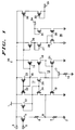
- FIG. 1 is a schematic of a first embodiment of the present invention.
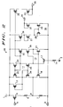
- FIG. 2 is a schematic of a second embodiment of the present invention.
- FIG. 3 is a partial block diagram of an adder circuit comprising the first embodiment.
- Figure 1 illustrates a voltage to current converter circuit 10 that is manufacturable using a standard CMOS process.
- a field effect transistor 4 has a source connected to an input terminal 3, a gate connected to an enable terminal 5, and a drain coupled to a voltage reference node 8 by a resistor 6, and the voltage reference node 8 is coupled to a supply voltage terminal 2 operating at ground potential by a resistor 7.
- the field effect transistor 4 and the resistor 6 and 7 comprise a voltage divider for providing a reference voltage (V REF ) at the voltage reference mode 8 with its magnitude determined by a conversion voltage (V CONV ) at the input terminal 3 and the ratio of the resistances of the resistors 6 and 7.
- a change in the value of the resistor 6 (R 6 ) can be offset by a corresponding change in the value of the resistor 7 (R 7 ) and vise versa if the two resistors 6 and 7 are placed in close proximity to one another.
- a stable reference voltage then, can be developed at the voltage reference node 8 by the use of monolithically integrated resistors.
- Other methods to provide the reference voltage could include using ratioed field effect transistors or by the use of switched capacitor circuits.
- the voltage to current converter circuit can be put into a low power stand-by mode by applying a logical 1 signal at the enable terminal 5, whereby field effect transistor 4 will be in its nonconducting state and no current will flow through the resistors 6 and 7 and thus the reference voltage will equal 0.0 volts.
- the linear reference current generator circuitry is comprised of a cascode current mirror 11, a current mirror 12, and devices 13, 14, 15, and 16.
- the cascode current mirror 11 comprises field effect transistors 22, 23, 24, and 25, and the current mirror 12 comprises field effect transistors 19 and 21.
- field effect transistor 23 forms a diode having a source connected to the input terminal 3, and a gate and a drain connected to a current reference node 18.
- the field effect transistor 22 having a source connected to the input terminal 3, a gate connected to the current reference node 18, and a drain connected to the drain of a field effect transistor 24, mirrors a linear reference current that is produced in the field effect transistor 23.
- the field effect transistor 24 forms a diode having a gate connected to a drain, and a source connected to the voltage reference node 8.
- the field effect transistor 25 having a drain connected to the current reference node 18, a gate connected to the gate of the field effect transistor 24, and a source connected to a gain terminal 17, mirrors the mirrored linear reference current flowing in the field effect transistor 24.
- the field effect transistor 21 forms a diode having a source connected to the supply voltage terminal 2, and a gate and a drain connected to a gate of a field effect transistor 19.
- the field effect transistor 19 having a source connected to the supply voltage terminal 2, and a drain connected to the voltage reference node 8, mirrors a feedback current flowing in the field effect transistor 21.
- a gain resistor 14 (R14) is coupled between the gain terminal 17 and the supply voltage terminal 2 and sets the magnitude of the linear reference current flowing in the cascode current mirror 11.
- the gain resistor 14 could be implemented as a monolithically integrated resistor on chip, or as a field effect transistor operated in its linear region. Alternatively, an external resistor (not monolithically integrated) could be used as the gain resistor 14 (providing excellent accuracy therewith).
- the field effect transistor 15 has a source connected to the input voltage terminal 3, a gate connected to the current reference node 18, and a drain connected to the source of a field effect transistor 16.
- the field effect transistor 16 has a gate connected to the gain terminal 17, and a drain connected to the drain of the field effect transistor 21.
- the field effect transistor 13 has a source connected to a supply voltage terminal 1 operating at a positive potential, such as V DD , and a gate and a drain connected to the source of the field effect transistor 24 for providing a start-up current to the cascode current mirror 11 when power is initially applied to the supply voltage terminals 1 and 2, and input terminal 3.
- An output stage comprises a current mirror 36, wherein a field effect transistor 28 forms a diode having a source connected to the supply voltage terminal 2, and a gate and a drain connected to the drain of a field effect transistor 27.
- a field effect transistor 29 has a source connected to the supply voltage terminal 2, a gate connected to the gate of the field effect transistor 28, and a drain connected to the source of a field effect transistor 31 for mirroring a reference sink current flowing in the field effect transistor 28.
- a field effect transistor 26 having a source connected to the input terminal 3, a gate connected to the current reference node 18, and a drain connected to a gate and a drain of the field effect transistor 27, sources the reference sink current to the current mirror 36.
- the field effect transistor 27 increases the impedance between the field effect transistor 26 and the supply voltage terminal 2.
- a field effect transistor 32 has a source connected to the input terminal 3, a gate connected to the current reference node 18, and a drain connected to the source of a field effect transistor 33 for providing a reference source current.
- the field effect transistor 31 has a gate and a drain connected to an output current sink terminal 34, and the field effect transistor 33 has a gate and drain connected to an output current source terminal 35.
- the purpose of the field effect transistors 31 and 33 is for increasing the output impedances at the output current sink and output current source terminals 34 and 35, respectively, therein providing the capability to couple the outputs of several voltage to current converter circuits together without degrading performance substantially.
- the reference voltage is determined by the ratio of the resistances of the resistors 6 and 7.
- a typical value of the reference voltage could be set at 1/4 the value of the conversion voltage. To accomplish this would require the resistance of R 6 to be three times the resistance of R 7 .
- the values of the resistors 6 and 7 should be chosen such that their parallel resistance is approximately 1/10 of the parallel impedance of the field effect transistors 19 and 24.
- the reference voltage By the action of the cascode current mirror 11, the reference voltage will be precisely tracked by a gain voltage at the gain terminal 17. A change in the conversion voltage causes a proportional change in the reference voltage which is accurately tracked at the gain terminal 17. The change in the gain voltage is accomplished by a linear change in the linear reference current through the cascode current mirror 11 since this current change is determined by the reference voltage.
- a change in the conversion voltage of 1 volt corresponds to a change in the linear reference current of 1 microamp.
- a different transconductance may be produced by varying the relationship of R 6 to R 7 and by varying the value of R14.
- the linear reference current flowing in the gain resistor 14 is reflected to the field effect transistor 15 by the current reference node 18.
- An undesired fluctuation in the linear reference current is mirrored back to the cascode current mirror 11 by the action of the current mirror 12.
- This fluctuation in the linear reference current flows through transistor 19 instead of being dissipated in the voltage divider network which would cause an unwanted change in the reference voltage.
- the closed loop operation of the linear reference current generator circuit keeps the reference voltage very precise.
- the linear reference current is reflected to the output stage's field effect transistors 26 and 32 by current reference node 18.
- the reference sink current flowing in the field effect transistor 26 will be mirrored in the field effect transistor 29 by the current mirror 36 when a load is connected to the output current sink terminal 34.
- the output current sink terminal 34 then, will sink an output sink current equal to the linear reference current or some ratio thereof.
- an output source current equal to the linear reference current or some ratio thereof will be sourced to the load.
- the first and second embodiments of the present invention are comprised of similar devices, but the second embodiment operates with the supply voltage terminals, 1 and 2, and input terminal 3 connected in a different manner as illustrated in FIG. 2.
- the difference in the second embodiment includes the sources of field effect transistors 4, 15, 22, 23, 26, and 32 being connected to the supply voltage terminal 1, the sources of field effect transistors 19, 21, 28, and 29 being connected to the input terminal 3, and the resistor 7 is coupled between the voltage reference node 8 and the input terminal 3.
- the resistor 6 is coupled between the supply voltage terminal 1 and the voltage reference node 8.
- V REF (V DD - V CONV )R 7 /(R 7 +R 6 ).
- the CMOS voltage to current converter circuit 20 provides a linear reference current for a conversion voltage that may vary from the V SS supply voltage less a V as to the V DD supply voltage less the sum of a N-channel and a P-channel threshold voltage.
- FIG. 3 An example of an adder implementation using the CMOS voltage to current converter circuit 10 is shown in FIG. 3.
- two voltage to current converter circuits 10 and 10′ are used to add two conversion voltages, V CONV1 and V CONV2 , applied at the input terminals 3 and 3′ respectively.
- Each CMOS voltage to current converter circuit 10 and 10′ may have a different gain as set by the gain resistors 14 and 14′ respectively.
- An output current source terminal 35 and 35′ of each CMOS voltage to current converter circuit 10 and 10′ is coupled to the supply voltage terminal 2 by a load resistor 37.
- An output source current, I 1 flowing from the output current source terminal 35 is added to an output source current, I 2 , flowing from the output current source terminal 35′, and the sum of these currents, I 3 , flows through the load resistor 37.
- the conversion voltages, V CONV1 and V CONV2 may vary from the sum of an N-channel and a P-channel threshold voltage above the V SS supply voltage to a V as above the V DD supply voltage.
- the voltage to current converter circuits 10 and 10′ in FIG 3 may be replaced by voltage to current converter circuits 20 and 20′ to provide operation wherein the conversion voltages V CONV1 and V CONV2 may vary from the sum of an N-channel and a P-channel threshold voltage below the V DD supply voltage to a V as below the V SS supply voltage.
- a subtractor circuit can be implemented by replacing the output current source terminal 35 connection of the voltage to current convert circuit 10 in figure 3 with a connection to the output current sink terminal 34. As a result, I 1 will be subtracted from I 2 .
- CMOS voltage to current converter circuit has been illustrated as an adder circuit, as an example, but may also be used to perform many other functions including multiplication, subtraction, etc.
- CMOS voltage to current converter circuit which provides a linear reference current accurate to the supply voltage rails, having a single ended input stable over a wide bandwidth without the need for compensation, offset correction, external feedback, or capacitive coupling.
Landscapes
- Engineering & Computer Science (AREA)
- Power Engineering (AREA)
- Amplifiers (AREA)
- Control Of Electrical Variables (AREA)
Claims (4)
- Komplementär-Metalloxid-Halbleiter (CMOS)-Spannungs-Stromumsetz-Schaltung, die umfaßt:
einen ersten Speisespannungsanschluß (1), der zur Aufnahme einer ersten Speisespannung geschaltet ist:
einen zweiten Speisespannungsanschluß (2), der zur Aufnahme einer zweiten Speisespannung geschaltet ist, wobei die erste Speisespannung höher ist als die zweite Speisespannung;
einen Eingangsanschluß, der zur Aufnahme einer Umsetzspannung geschaltet ist;
einen Ausgangsstromsenkanschluß (35);
einen Ausgangsstromquellenanschluß (34);
Spannungsteilereinrichtung (4, 6, 7), die zwischen den zweiten Speisespannungsanschluß und den Eingangsanschluß geschaltet ist, wobei die Umsetzspannung die Energie für die CMOS-Schaltung liefert und innerhalb eines Bereichs schwanken kann, der von zwei Schwellenspannungen, die über der zweiten Speisespannung liegen, bis zum Potential einer Gate-Source-Verbindung eines Transistors reicht, das über der ersten Speisespannung liegt, wobei die Spannungsteilereinrichtung einen Spannungsreferenzknoten (8) hat, der eine Referenzspannung in Bezug auf die an den Eingangsanschluß angelegte Umsetzspannung liefert;
Spannungs-Stromumsetz-Einrichtung (11, 12, 14, 15, 16), die an den ersten und den zweiten Speisespannungsanschluß und den Eingangsanschluß geschaltet ist, und zur Lieferung eines linearen Referenzstroms" dessen Größe sich in Reaktion auf eine entsprechende Änderung der Umsetzspannung linear ändert, an den Spannungsreferenzknoten geschaltet ist; und
Ausgangseinrichtung (26-29, 31-33), die zwischen dem zweiten Speisespannungsanschluß und dem Eingangsanschluß gespeist wird, an die Spannung-Stromumsetz-Einrichtung geschaltet ist, und am Ausgangsstromsenkanschluß und am Ausgangsstromquellenanschluß einen Ausgangssenkstrom bzw. einen Ausgangsquellenstrom liefert, wobei die Größe des Ausgangssenkstroms und die Größe des Ausgangsquellenstroms ein Teil der Größe des linearen Referenzstroms sind. - CMOS-Schaltung nach Anspruch 1, wobei die Spannung-Stromumsetz-Einrichtung umfaßt:
einen Verstärkungsanschluß (17);
einen Verstärkungswiderstand (14) , der zwischen den Verstärkungsanschluß und den zweiten Speisespannungsanschluß geschaltet ist;
eine erste Strom-Spiegeleinrichtung (11), die zwischen den Eingangsanschluß und den Verstärkungsanschluß geschaltet ist, an den Spannungsreferenzknoten (8) geschaltet ist, und einen linearen Referenzstrom erzeugt, wobei der Widerstandswert des Verstärkungswiderstandes (14) zusammen mit der Größe der Umsetzspannung die Größe des linearen Referenzstroms bestimmt, der in der ersten Strom-Spiegeleinrichtung (11) fließt;
eine zweite Strom-Spiegeleinrichtung (12) , die an den zweiten Speisespannungsanschluß und den Spannungsreferenzknoten (8) geschaltet ist, und einen Rückkopplungsstrom zur ersten Strom-Spiegeleinrichtung (11) liefert;
einen ersten Feldeffekttransistor (13) , dessen Source an den ersten Speisespannungsanschluß geschaltet ist, und dessen Gate und Drain an die erste Strom-Spiegeleinrichtung (11) geschaltet sind;
einen zweiten Feldeffekttransistor (15) , dessen Gate an die erste Strom-Spiegeleinrichtung geschaltet ist, dessen Source an den Eingangsanschluß geschaltet ist, und der einen Drain hat; und
einen dritten Feldeffekttransistor (16) dessen Source an den Drain des zweiten Feldeffekttransistors geschaltet ist, dessen Gate an den Verstärkungsanschluß geschaltet ist, und dessen Drain an die zweite Strom-Spiegeleinrichtung geschaltet ist. - CMOS-Schaltung nach Anspruch 2, wobei die Ausgangseinrichtung (26-29, 31-33) umfaßt:
eine dritte Strom-Spiegeleinrichtung (36), die zwischen den zweiten Speisespannungsanschluß und den Ausgangsstromsenkanschluß geschaltet ist, und einen Strom vom Ausgangsstromsenkanschluß senkt;
einen vierten Feldeffekttransistor (26), dessen Source an den Eingangsanschluß geschaltet ist, dessen Gate an die Spannung-Stromumsetz-Einrichtung geschaltet ist, und der einen Drain hat;
einen fünften Feldeffekttransistor (27), dessen Source und dessen Gate an den Drain des vierten Feldeffekttransistors (26) geschaltet sind, und dessen Drain an die dritte Strom-Spiegeleinrichtung geschaltet ist; und
einen sechsten Feldeffekttransistor (32), dessen Source an den Eingangsanschluß geschaltet ist, dessen Gate an das Gate des vierten Feldeffekttransistors (26) geschaltet ist, und dessen Drain an den Ausgangsstromquellenanschluß (35) geschaltet ist . - Komplementär-Metalloxid-Halbleiter (CMOS)-Spannung-Stromumsetz-Schaltung, die umfaßt:
einen ersten Speisespannungsanschluß (1);
einen zweiten Speisespannungsanschluß (2);
einen Eingangsanschluß (3);
einen Ausgangsstromsenkanschluß (35);
einen Ausgangsstromquellenanschluß (34);
einen Verstärkungsanschluß (17);
einen ersten Widerstand (6), der zwischen den Eingangsanschluß und den Spannungsreferenzknoten (8) geschaltet ist;
einen zweiten Widerstand (7) , der zwischen den Spannungsreferenzknoten (8) und den zweiten Speisespannungsanschluß geschaltet ist;
einen ersten Feldeffekttransistor (13), dessen Source an den ersten Speisespannungsanschluß geschaltet ist, und der ein Gate und einen Drain hat;
einen zweiten Feldeffekttransistor (15) , dessen Source an den Eingangsanschluß geschaltet ist, dessen Gate an einen Stromreferenzknoten (18) geschaltet ist, und der einen Drain hat;
einen dritten Feldeffekttransistor (16) , dessen Source an den Drain des zweiten Feldeffekttransistors geschaltet ist, dessen Gate an den Verstärkungsanschluß geschaltet ist, und der einen Drain hat;
einen vierten Feldeffekttransistor (26), dessen Source an den Eingangsanschluß geschaltet ist, dessen Gate an den Stromreferenzknoten geschaltet, und der einen Drain hat;
einen fünften Feldeffekttransistor (27), dessen Source und dessen Gate an den Drain des vierten Feldeffekttransistors geschaltet sind, und der einen Drain hat;
einen sechsten Feldeffekttransistor (32), dessen Source an den Eingangsanschluß geschaltet ist, dessen Gate an den Stromreferenzknoten (18) geschaltet ist, und dessen Drain an den Ausgangsspannungsquellenanschluß (35) geschaltet ist;
einen siebenten Feldeffekttransistor (22), dessen Source an den Eingangsanschluß geschaltet ist, dessen Gate an den Stromreferenzknoten (18) geschaltet ist, und dessen Drain an das Gate und den Drain des ersten Feldeffekttransistors geschaltet ist;
einen achten Feldeffekttransistor (23), dessen Source an den Eingangsanschluß geschaltet ist und dessen Gate und dessen Drain an den Stromreferenzknoten (18) geschaltet sind;
einen neunten Feldeffekttransistor (24), dessen Source und dessen Gate an den Drain des siebenten Feldeffekttransistors geschaltet sind, und dessen Drain an den Spannungsreferenzknoten (8) geschaltet ist;
einen zehnten Feldeffekttransistor (25), dessen Drain an den Stromreferenzknoten (18) geschaltet ist, dessen Gate an das Gate des neunten Feldeffekttransistor (24) geschaltet ist, und dessen Source an den Verstärkungsanschluß (17) geschaltet ist;
einen Verstärkungswiderstand (14) , der zwischen den Verstärkungsanschluß (17) und den zweiten Speisespannungsanschluß geschaltet ist;
einen elften Feldeffekttransistor (21), dessen Gate und dessen Drain an den Drain des dritten Feldeffekttransistors (16) geschaltet sind, und dessen Source an den zweiten Speisespannungsanschluß geschaltet ist;
einen zwölften Feldeffekttransistor (19), dessen Drain an den Spannungsreferenzknoten (8) geschaltet ist, dessen Gate an das Gate des elften Feldeffekttransistors (21) geschaltet ist, und dessen Source an den zweiten Speisespannungsanschluß geschaltet ist;
einen dreizehnten Feldeffekttransistor (28), dessen Gate und dessen Drain an den Drain des fünften Feldeffekttransistors (27) geschaltet sind, und dessen Source an den zweiten Speisespannungsanschluß geschaltet ist; und
einen vierzehnten Feldeffekttransistor (29), dessen Drain an den Ausgangsstromsenkanschluß (34) geschaltet ist, dessen Gate an das Gate des dreizehnten Feldeffekttransistors (28) geschaltet ist, und dessen Source an den zweiten Speisespannungsanschluß geschaltet ist.
Applications Claiming Priority (2)
| Application Number | Priority Date | Filing Date | Title |
|---|---|---|---|
| US07/181,607 US4835487A (en) | 1988-04-14 | 1988-04-14 | MOS voltage to current converter |
| US181607 | 1994-01-13 |
Publications (3)
| Publication Number | Publication Date |
|---|---|
| EP0337444A2 EP0337444A2 (de) | 1989-10-18 |
| EP0337444A3 EP0337444A3 (en) | 1990-08-01 |
| EP0337444B1 true EP0337444B1 (de) | 1992-10-21 |
Family
ID=22665005
Family Applications (1)
| Application Number | Title | Priority Date | Filing Date |
|---|---|---|---|
| EP89106559A Expired - Lifetime EP0337444B1 (de) | 1988-04-14 | 1989-04-13 | Spannungs-Stromumsetzer mit MOS-Transistoren |
Country Status (7)
| Country | Link |
|---|---|
| US (1) | US4835487A (de) |
| EP (1) | EP0337444B1 (de) |
| JP (1) | JPH01311608A (de) |
| KR (1) | KR890016749A (de) |
| DE (1) | DE68903243T2 (de) |
| HK (1) | HK85895A (de) |
| SG (1) | SG59887G (de) |
Cited By (1)
| Publication number | Priority date | Publication date | Assignee | Title |
|---|---|---|---|---|
| US11323085B2 (en) | 2019-09-04 | 2022-05-03 | Analog Devices International Unlimited Company | Voltage-to-current converter with complementary current mirrors |
Families Citing this family (18)
| Publication number | Priority date | Publication date | Assignee | Title |
|---|---|---|---|---|
| EP0353508B1 (de) * | 1988-07-22 | 1994-09-21 | Siemens Aktiengesellschaft | ECL-CMOS-Wandler |
| US4978905A (en) * | 1989-10-31 | 1990-12-18 | Cypress Semiconductor Corp. | Noise reduction output buffer |
| US5165054A (en) * | 1990-12-18 | 1992-11-17 | Synaptics, Incorporated | Circuits for linear conversion between currents and voltages |
| US5481180A (en) * | 1991-09-30 | 1996-01-02 | Sgs-Thomson Microelectronics, Inc. | PTAT current source |
| US5550495A (en) * | 1994-05-12 | 1996-08-27 | Sierra Semiconductor Corporation | All MOS voltage to current converter |
| US5841866A (en) * | 1994-09-30 | 1998-11-24 | Microchip Technology Incorporated | Secure token integrated circuit and method of performing a secure authentication function or transaction |
| KR0134661B1 (ko) * | 1995-04-24 | 1998-04-25 | 김광호 | 전위전류 변환기 |
| US5594326A (en) * | 1995-06-07 | 1997-01-14 | Analog Devices, Inc. | Sub-rail voltage regulator with low stand-by current and high load current |
| US5610505A (en) * | 1995-08-31 | 1997-03-11 | Lucent Technologies, Inc. | Voltage-to-current converter with MOS reference resistor |
| US5978249A (en) * | 1997-12-17 | 1999-11-02 | Motorola Inc. | High impedance signal conversion circuit and method |
| KR100323196B1 (ko) * | 1999-09-03 | 2002-02-20 | 박종섭 | 모스 전계효과 트랜지스터를 이용한 정밀전파정류기 |
| KR100368982B1 (ko) * | 1999-11-30 | 2003-01-24 | 주식회사 하이닉스반도체 | 씨모스 정전류 레퍼런스 회로 |
| DE50012856D1 (de) | 2000-02-15 | 2006-07-06 | Infineon Technologies Ag | Spannungs-Strom-Wandler |
| US6995612B1 (en) * | 2003-12-15 | 2006-02-07 | Sun Microsystems, Inc. | Circuit for reducing current mirror mismatch due to gate leakage current |
| TWI341636B (en) * | 2007-10-17 | 2011-05-01 | Mstar Semiconductor Inc | Circuit for protecting nmos device from voltage stress |
| CN107491132B (zh) * | 2016-06-12 | 2019-11-05 | 中芯国际集成电路制造(上海)有限公司 | 电压电流转换电路 |
| CN112558670B (zh) * | 2020-12-21 | 2022-03-04 | 哈尔滨天达控制股份有限公司 | 一种高精度电压电流变换器 |
| FR3147917A1 (fr) * | 2023-04-17 | 2024-10-18 | Stmicroelectronics International N.V. | Circuit intégré comprenant une source de courant d’intensité modulée et procédé de génération correspondant. |
Family Cites Families (7)
| Publication number | Priority date | Publication date | Assignee | Title |
|---|---|---|---|---|
| US3953807A (en) * | 1973-08-09 | 1976-04-27 | Rca Corporation | Current amplifier |
| DE2459271C3 (de) * | 1974-12-14 | 1980-08-28 | Philips Patentverwaltung Gmbh, 2000 Hamburg | Schaltungsanordnung zum Erzeugen eines kompensierten Gleichstromes |
| JPS5652420A (en) * | 1979-10-03 | 1981-05-11 | Toshiba Corp | Constant-current circuit |
| US4612496A (en) * | 1984-10-01 | 1986-09-16 | Motorola, Inc. | Linear voltage-to-current converter |
| US4618816A (en) * | 1985-08-22 | 1986-10-21 | National Semiconductor Corporation | CMOS ΔVBE bias current generator |
| KR970000909B1 (en) * | 1985-09-02 | 1997-01-21 | Siemens Ag | Controlled current source apparatus |
| US4700144A (en) * | 1985-10-04 | 1987-10-13 | Gte Communication Systems Corporation | Differential amplifier feedback current mirror |
-
1988
- 1988-04-14 US US07/181,607 patent/US4835487A/en not_active Expired - Fee Related
-
1989
- 1989-04-11 KR KR1019890004733A patent/KR890016749A/ko not_active Withdrawn
- 1989-04-13 EP EP89106559A patent/EP0337444B1/de not_active Expired - Lifetime
- 1989-04-13 DE DE8989106559T patent/DE68903243T2/de not_active Expired - Fee Related
- 1989-04-13 SG SG1995906400A patent/SG59887G/en unknown
- 1989-04-14 JP JP1093286A patent/JPH01311608A/ja active Pending
-
1995
- 1995-06-01 HK HK85895A patent/HK85895A/xx unknown
Cited By (2)
| Publication number | Priority date | Publication date | Assignee | Title |
|---|---|---|---|---|
| US11323085B2 (en) | 2019-09-04 | 2022-05-03 | Analog Devices International Unlimited Company | Voltage-to-current converter with complementary current mirrors |
| US12506454B2 (en) | 2019-09-04 | 2025-12-23 | Analog Devices International Unlimited Company | Voltage-to-current converter with complementary current mirrors |
Also Published As
| Publication number | Publication date |
|---|---|
| EP0337444A3 (en) | 1990-08-01 |
| DE68903243T2 (de) | 1993-04-22 |
| SG59887G (en) | 1995-09-01 |
| US4835487A (en) | 1989-05-30 |
| KR890016749A (ko) | 1989-11-30 |
| EP0337444A2 (de) | 1989-10-18 |
| DE68903243D1 (de) | 1992-11-26 |
| JPH01311608A (ja) | 1989-12-15 |
| HK85895A (en) | 1995-06-09 |
Similar Documents
| Publication | Publication Date | Title |
|---|---|---|
| US4835487A (en) | MOS voltage to current converter | |
| Kaulberg | A CMOS current-mode operational amplifier | |
| KR100377064B1 (ko) | 적응바이어서회로및공통모드궤환회로를갖는완전차동폴디드캐스코드씨모오스(cmos)오피앰프(opamp)회로 | |
| US5422529A (en) | Differential charge pump circuit with high differential and low common mode impedance | |
| JP3318725B2 (ja) | アナログフィルタ回路 | |
| US5929621A (en) | Generation of temperature compensated low noise symmetrical reference voltages | |
| US5519310A (en) | Voltage-to-current converter without series sensing resistor | |
| EP0639889B1 (de) | Voll differentieller Operationsverstärker mit niedriger Versorgungsspannung | |
| JP3505120B2 (ja) | 絶対温度、容量及びクロック周波数に比例する基準信号を発生するスイッチトキャパシタバイアス回路 | |
| US3984780A (en) | CMOS voltage controlled current source | |
| US6057727A (en) | Accurate constant current generator | |
| US4573020A (en) | Fully differential operational amplifier with D.C. common-mode feedback | |
| KR100275177B1 (ko) | 저전압차동증폭기 | |
| US4714845A (en) | Low offset voltage follower circuit | |
| KR0177511B1 (ko) | 선형 cmos 출력단 | |
| US4585951A (en) | Precision triangle waveform generator | |
| US5043652A (en) | Differential voltage to differential current conversion circuit having linear output | |
| US10554218B1 (en) | Sigma-delta modulator | |
| US6717451B1 (en) | Precision analog level shifter with programmable options | |
| KR100219037B1 (ko) | 선형화된 저항성을 이용한 모스펫 아날로그 곱셈기 | |
| US11742812B2 (en) | Output pole-compensated operational amplifier | |
| EP0618674B1 (de) | Spannung-Strom-Wandlerschaltung | |
| US6583746B2 (en) | A/D converter with high speed input circuit | |
| JPS63185107A (ja) | 電圧制御型電流源 | |
| JP3081210B2 (ja) | 線形利得増幅回路 |
Legal Events
| Date | Code | Title | Description |
|---|---|---|---|
| PUAI | Public reference made under article 153(3) epc to a published international application that has entered the european phase |
Free format text: ORIGINAL CODE: 0009012 |
|
| AK | Designated contracting states |
Kind code of ref document: A2 Designated state(s): DE FR GB IT |
|
| PUAL | Search report despatched |
Free format text: ORIGINAL CODE: 0009013 |
|
| AK | Designated contracting states |
Kind code of ref document: A3 Designated state(s): DE FR GB IT |
|
| 17P | Request for examination filed |
Effective date: 19910131 |
|
| 17Q | First examination report despatched |
Effective date: 19910722 |
|
| GRAA | (expected) grant |
Free format text: ORIGINAL CODE: 0009210 |
|
| AK | Designated contracting states |
Kind code of ref document: B1 Designated state(s): DE FR GB IT |
|
| PG25 | Lapsed in a contracting state [announced via postgrant information from national office to epo] |
Ref country code: IT Free format text: LAPSE BECAUSE OF FAILURE TO SUBMIT A TRANSLATION OF THE DESCRIPTION OR TO PAY THE FEE WITHIN THE PRE;WARNING: LAPSES OF ITALIAN PATENTS WITH EFFECTIVE DATE BEFORE 2007 MAY HAVE OCCURRED AT ANY TIME BEFORE 2007. THE CORRECT EFFECTIVE DATE MAY BE DIFFERENT FROM THE ONE RECORDED.SCRIBED TIME-LIMIT Effective date: 19921021 Ref country code: FR Effective date: 19921021 |
|
| REF | Corresponds to: |
Ref document number: 68903243 Country of ref document: DE Date of ref document: 19921126 |
|
| EN | Fr: translation not filed | ||
| PLBE | No opposition filed within time limit |
Free format text: ORIGINAL CODE: 0009261 |
|
| STAA | Information on the status of an ep patent application or granted ep patent |
Free format text: STATUS: NO OPPOSITION FILED WITHIN TIME LIMIT |
|
| 26N | No opposition filed | ||
| PGFP | Annual fee paid to national office [announced via postgrant information from national office to epo] |
Ref country code: GB Payment date: 19950418 Year of fee payment: 7 |
|
| PGFP | Annual fee paid to national office [announced via postgrant information from national office to epo] |
Ref country code: DE Payment date: 19950502 Year of fee payment: 7 |
|
| PG25 | Lapsed in a contracting state [announced via postgrant information from national office to epo] |
Ref country code: GB Effective date: 19960413 |
|
| GBPC | Gb: european patent ceased through non-payment of renewal fee |
Effective date: 19960413 |
|
| PG25 | Lapsed in a contracting state [announced via postgrant information from national office to epo] |
Ref country code: DE Effective date: 19970101 |