EP0337540B1 - Combinaison d'un support et d'un corps semi-conducteur et son procédé de fabrication - Google Patents
Combinaison d'un support et d'un corps semi-conducteur et son procédé de fabrication Download PDFInfo
- Publication number
- EP0337540B1 EP0337540B1 EP89200844A EP89200844A EP0337540B1 EP 0337540 B1 EP0337540 B1 EP 0337540B1 EP 89200844 A EP89200844 A EP 89200844A EP 89200844 A EP89200844 A EP 89200844A EP 0337540 B1 EP0337540 B1 EP 0337540B1
- Authority
- EP
- European Patent Office
- Prior art keywords
- semiconductor body
- support
- metal layer
- projecting part
- combination
- Prior art date
- Legal status (The legal status is an assumption and is not a legal conclusion. Google has not performed a legal analysis and makes no representation as to the accuracy of the status listed.)
- Expired - Lifetime
Links
Images
Classifications
-
- G—PHYSICS
- G01—MEASURING; TESTING
- G01L—MEASURING FORCE, STRESS, TORQUE, WORK, MECHANICAL POWER, MECHANICAL EFFICIENCY, OR FLUID PRESSURE
- G01L9/00—Measuring steady of quasi-steady pressure of fluid or fluent solid material by electric or magnetic pressure-sensitive elements; Transmitting or indicating the displacement of mechanical pressure-sensitive elements, used to measure the steady or quasi-steady pressure of a fluid or fluent solid material, by electric or magnetic means
- G01L9/0041—Transmitting or indicating the displacement of flexible diaphragms
- G01L9/0042—Constructional details associated with semiconductive diaphragm sensors, e.g. etching, or constructional details of non-semiconductive diaphragms
-
- H—ELECTRICITY
- H10—SEMICONDUCTOR DEVICES; ELECTRIC SOLID-STATE DEVICES NOT OTHERWISE PROVIDED FOR
- H10W—GENERIC PACKAGES, INTERCONNECTIONS, CONNECTORS OR OTHER CONSTRUCTIONAL DETAILS OF DEVICES COVERED BY CLASS H10
- H10W72/00—Interconnections or connectors in packages
- H10W72/30—Die-attach connectors
-
- H—ELECTRICITY
- H10—SEMICONDUCTOR DEVICES; ELECTRIC SOLID-STATE DEVICES NOT OTHERWISE PROVIDED FOR
- H10W—GENERIC PACKAGES, INTERCONNECTIONS, CONNECTORS OR OTHER CONSTRUCTIONAL DETAILS OF DEVICES COVERED BY CLASS H10
- H10W70/00—Package substrates; Interposers; Redistribution layers [RDL]
- H10W70/60—Insulating or insulated package substrates; Interposers; Redistribution layers
- H10W70/67—Insulating or insulated package substrates; Interposers; Redistribution layers characterised by their insulating layers or insulating parts
- H10W70/68—Shapes or dispositions thereof
- H10W70/681—Shapes or dispositions thereof comprising holes not having chips therein, e.g. for outgassing, underfilling or bond wire passage
-
- H—ELECTRICITY
- H10—SEMICONDUCTOR DEVICES; ELECTRIC SOLID-STATE DEVICES NOT OTHERWISE PROVIDED FOR
- H10W—GENERIC PACKAGES, INTERCONNECTIONS, CONNECTORS OR OTHER CONSTRUCTIONAL DETAILS OF DEVICES COVERED BY CLASS H10
- H10W72/00—Interconnections or connectors in packages
- H10W72/071—Connecting or disconnecting
- H10W72/072—Connecting or disconnecting of bump connectors
- H10W72/07231—Techniques
- H10W72/07236—Soldering or alloying
-
- H—ELECTRICITY
- H10—SEMICONDUCTOR DEVICES; ELECTRIC SOLID-STATE DEVICES NOT OTHERWISE PROVIDED FOR
- H10W—GENERIC PACKAGES, INTERCONNECTIONS, CONNECTORS OR OTHER CONSTRUCTIONAL DETAILS OF DEVICES COVERED BY CLASS H10
- H10W72/00—Interconnections or connectors in packages
- H10W72/071—Connecting or disconnecting
- H10W72/073—Connecting or disconnecting of die-attach connectors
- H10W72/07331—Connecting techniques
- H10W72/07337—Connecting techniques using a polymer adhesive, e.g. an adhesive based on silicone or epoxy
-
- H—ELECTRICITY
- H10—SEMICONDUCTOR DEVICES; ELECTRIC SOLID-STATE DEVICES NOT OTHERWISE PROVIDED FOR
- H10W—GENERIC PACKAGES, INTERCONNECTIONS, CONNECTORS OR OTHER CONSTRUCTIONAL DETAILS OF DEVICES COVERED BY CLASS H10
- H10W72/00—Interconnections or connectors in packages
- H10W72/20—Bump connectors, e.g. solder bumps or copper pillars; Dummy bumps; Thermal bumps
- H10W72/241—Dispositions, e.g. layouts
-
- Y—GENERAL TAGGING OF NEW TECHNOLOGICAL DEVELOPMENTS; GENERAL TAGGING OF CROSS-SECTIONAL TECHNOLOGIES SPANNING OVER SEVERAL SECTIONS OF THE IPC; TECHNICAL SUBJECTS COVERED BY FORMER USPC CROSS-REFERENCE ART COLLECTIONS [XRACs] AND DIGESTS
- Y10—TECHNICAL SUBJECTS COVERED BY FORMER USPC
- Y10T—TECHNICAL SUBJECTS COVERED BY FORMER US CLASSIFICATION
- Y10T29/00—Metal working
- Y10T29/49—Method of mechanical manufacture
- Y10T29/49002—Electrical device making
- Y10T29/49117—Conductor or circuit manufacturing
- Y10T29/49124—On flat or curved insulated base, e.g., printed circuit, etc.
- Y10T29/4913—Assembling to base an electrical component, e.g., capacitor, etc.
- Y10T29/49139—Assembling to base an electrical component, e.g., capacitor, etc. by inserting component lead or terminal into base aperture
- Y10T29/4914—Assembling to base an electrical component, e.g., capacitor, etc. by inserting component lead or terminal into base aperture with deforming of lead or terminal
-
- Y—GENERAL TAGGING OF NEW TECHNOLOGICAL DEVELOPMENTS; GENERAL TAGGING OF CROSS-SECTIONAL TECHNOLOGIES SPANNING OVER SEVERAL SECTIONS OF THE IPC; TECHNICAL SUBJECTS COVERED BY FORMER USPC CROSS-REFERENCE ART COLLECTIONS [XRACs] AND DIGESTS
- Y10—TECHNICAL SUBJECTS COVERED BY FORMER USPC
- Y10T—TECHNICAL SUBJECTS COVERED BY FORMER US CLASSIFICATION
- Y10T29/00—Metal working
- Y10T29/49—Method of mechanical manufacture
- Y10T29/49002—Electrical device making
- Y10T29/49117—Conductor or circuit manufacturing
- Y10T29/49124—On flat or curved insulated base, e.g., printed circuit, etc.
- Y10T29/49147—Assembling terminal to base
- Y10T29/49151—Assembling terminal to base by deforming or shaping
- Y10T29/49153—Assembling terminal to base by deforming or shaping with shaping or forcing terminal into base aperture
Definitions
- the invention relates to a combination of a support and a semiconductor body, in which a deformable metal layer is disposed between the semiconductor body and the support and the semiconductor body is connected to the support by pressing the semiconductor body and the support against each other other under pressure after heating the metal layer.
- Such a combination of a semiconductor body and a support is known from Netherlands Patent Application NL-A- 7415668, which corresponds to FR-A- 2 293 704.
- the metal layer is enclosed between two parallel extending boundary surfaces of the support and the semiconductor body.
- connection is satisfactory, but in certain cases it may be desirable to realize a more rigid connection between the support and the semiconductor body.
- the semiconductor body is provided at its surface facing the support with at least one projecting part, which is embedded in the metal layer.
- the projection then has a closed contour, by means of this projection a particularly satisfactory vacuum-tight connection can further be obtained between the semiconductor body and the support, which may be important, for example, in pressure sensors and the like.
- a further aspect of the invention relates to a method of connecting a semiconductor body to a support, in which a deformable metal layer is provided between the semiconductor body and the support and the semiconductor body is connected to the support by pressing the semiconductor body and the support against each other under pressure at an elevated temperature.
- a projecting part integral with the semiconductor body is formed on the semiconductor body on the side to face the support and this projecting part is pressed into the metal layer when providing the semiconductor.
- a semiconductor body to be manufactured in a simple manner can be secured very firmly to a support.
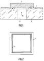
- a semiconductor body 1 is provided on a support 3 with the interposition of a metal layer 2.
- the insulating support 3 may be made, for example, of glass.
- the metal layer 2 will consist of aluminium and will generally have a thickness of the order of 10 ⁇ m.
- the semiconductor body 1 is provided on its side facing the support 3 with a projection, which is constituted in the embodiment shown by a continuous projecting edge 4 having a cross-section of triangular form.
- the height of this projection projecting beyond the boundary surface of the semiconductor body is about half the thickness of the metal layer 2 in the non-deformed state.
- the projection 4 can be formed in a simple and efficacious manner by removing parts of the starting material located around the projection by etching.
- the metal layer 2 is arranged between the support and the semiconductor body 1, after which, whilst heating the metal layer 2, the semiconductor body 1 and the support 3 are pressed towards each other, the continuous projection 4 penetrating in the manner shown in Figure 1 into the metal layer.
- the metal layer 2 may be applied to the support 3, for example by vapour deposition.
- the projection 4 it is not necessary for the projection 4 to form a closed contour, while it is also possible that several projections located at a certain relative distance are provided.
- a projection forming a closed contour is particularly advantageous, however, if the projection, as is the case in the embodiment shown in Figure 2, surrounds a recess 5 provided in the support 3 and different pressures prevail on either side of the support. In fact it has been found that by the use of a projection forming a closed contour a particularly satisfactory gas-tight connection can be obtained between the support and the semiconductor body.
- the form of the cross-section of the projection 4 may also be different from the triangular form shown; for example, viewed in cross-section the projection may have the form of a truncated cone.
- the projection is provided with an aluminium coating so that, when the semiconductor body is contacted with the metal layer consisting of aluminium, a connection of aluminium on aluminium is obtained.
- the projection may then also be provided with a silicon oxide layer, on which the aluminium coating is formed.
Landscapes
- Chemical & Material Sciences (AREA)
- Analytical Chemistry (AREA)
- Physics & Mathematics (AREA)
- General Physics & Mathematics (AREA)
- Pressure Sensors (AREA)
- Measuring Fluid Pressure (AREA)
- Internal Circuitry In Semiconductor Integrated Circuit Devices (AREA)
- Pressure Welding/Diffusion-Bonding (AREA)
- Cooling Or The Like Of Semiconductors Or Solid State Devices (AREA)
- Die Bonding (AREA)
Claims (7)
- Dispositif semiconducteur comportant un corps semiconducteur (1) et un support (3) reliés entre eux par une liaison par thermocompression comportant une couche métallique déformable (2), caractérisée en ce que, sur sa surface située du côté du support (3), le corps semiconducteur (1) est pourvu d'au moins une partie saillante (4), noyée dans la couche métallique (2).
- Dispositif semiconducteur selon la revendication 1, caractérisé en ce que la partie saillante (4) forme un contour fermé et enferme l'extrémité d'un passage formé dans le support (3).
- Dispositif semiconducteur selon la revendication 1 ou 2, caractérisé en ce que, vue en section transversale, la partie saillante (4) a une forme sensiblement triangulaire.
- Procédé de liaison d'un corps semiconducteur (1) à un support (3), suivant lequel on forme une couche métallique déformable (2) entre le corps semiconducteur (1) et le support (3) en pressant le corps semiconducteur (1) et le support (3) sous pression l'un contre l'autre à une température élevée, caractérisé en ce que avant la mise en place du corps semiconducteur (1) sur le support (3), sur la face devant être située du côté du support (3), on forme au moins une partie saillante (4) d'une seule pièce avec le corps semiconducteur (1) et en ce qu'on presse cette partie saillante (4) dans la couche métallique (2) lors de la mise en place du corps semiconducteur (1) sur le support (3).
- Procédé selon la revendication 4, caractérisé en ce que la partie saillante (4) est formée sur le corps semiconducteur par attaque chimique.
- Procédé selon la revendication 4 ou 5, caractérisé en ce que, avant la mise en place du corps semiconducteur (1) sur le support (3), on recouvre la partie saillante (4) d'aluminium.
- Procédé selon la revendication 4, 5 ou 6, caractérisé en ce que la hauteur de la partie saillante (4) formée sur le corps semiconducteur (1) est environ égale à la moitié de l'épaisseur que présente la couche métallique (2) dans l'état non déformé.
Applications Claiming Priority (2)
| Application Number | Priority Date | Filing Date | Title |
|---|---|---|---|
| NL8800901A NL8800901A (nl) | 1988-04-08 | 1988-04-08 | Combinatie van een drager en een halfgeleiderlichaam en werkwijze voor het vervaardigen van een dergelijke combinatie. |
| NL8800901 | 1988-04-08 |
Publications (2)
| Publication Number | Publication Date |
|---|---|
| EP0337540A1 EP0337540A1 (fr) | 1989-10-18 |
| EP0337540B1 true EP0337540B1 (fr) | 1994-10-12 |
Family
ID=19852089
Family Applications (1)
| Application Number | Title | Priority Date | Filing Date |
|---|---|---|---|
| EP89200844A Expired - Lifetime EP0337540B1 (fr) | 1988-04-08 | 1989-04-03 | Combinaison d'un support et d'un corps semi-conducteur et son procédé de fabrication |
Country Status (5)
| Country | Link |
|---|---|
| US (2) | US4929999A (fr) |
| EP (1) | EP0337540B1 (fr) |
| JP (1) | JPH01310545A (fr) |
| DE (1) | DE68918741T2 (fr) |
| NL (1) | NL8800901A (fr) |
Families Citing this family (13)
| Publication number | Priority date | Publication date | Assignee | Title |
|---|---|---|---|---|
| JPH0770806B2 (ja) * | 1990-08-22 | 1995-07-31 | 株式会社エーユーイー研究所 | 超音波溶着による電子回路およびその製造方法 |
| US5585282A (en) * | 1991-06-04 | 1996-12-17 | Micron Technology, Inc. | Process for forming a raised portion on a projecting contact for electrical testing of a semiconductor |
| US5385869A (en) * | 1993-07-22 | 1995-01-31 | Motorola, Inc. | Semiconductor chip bonded to a substrate and method of making |
| US5478779A (en) | 1994-03-07 | 1995-12-26 | Micron Technology, Inc. | Electrically conductive projections and semiconductor processing method of forming same |
| US5326428A (en) | 1993-09-03 | 1994-07-05 | Micron Semiconductor, Inc. | Method for testing semiconductor circuitry for operability and method of forming apparatus for testing semiconductor circuitry for operability |
| DE4409068C2 (de) * | 1994-03-14 | 1998-05-28 | Hartmann & Braun Ag | Bondverfahren und damit hergestellte Bondverbindung |
| DE4433689C2 (de) * | 1994-09-21 | 1996-07-11 | Siemens Ag | Chipkonfiguration und Verwendung eines entsprechenden Chips |
| FR2738395B1 (fr) * | 1995-08-31 | 1997-10-10 | Commissariat Energie Atomique | Dispositif autoporte pour la propagation d'ondes hyperfrequences et procedes de realisation d'un tel dispositif |
| JPH10270496A (ja) * | 1997-03-27 | 1998-10-09 | Hitachi Ltd | 電子装置、情報処理装置、半導体装置並びに半導体チップの実装方法 |
| FR2775810B1 (fr) * | 1998-03-09 | 2000-04-28 | Gemplus Card Int | Procede de fabrication de cartes sans contact |
| US6078103A (en) * | 1998-10-29 | 2000-06-20 | Mcdonnell Douglas Corporation | Dimpled contacts for metal-to-semiconductor connections, and methods for fabricating same |
| JP4159778B2 (ja) * | 2001-12-27 | 2008-10-01 | 三菱電機株式会社 | Icパッケージ、光送信器及び光受信器 |
| US9076674B2 (en) * | 2012-09-25 | 2015-07-07 | Intermolecular, Inc. | Method and apparatus for improving particle performance |
Citations (2)
| Publication number | Priority date | Publication date | Assignee | Title |
|---|---|---|---|---|
| EP0259035A2 (fr) * | 1986-08-28 | 1988-03-09 | Stc Plc | Lien de brasure entre un composant électrique et un substrat |
| EP0262580A2 (fr) * | 1986-09-25 | 1988-04-06 | Kabushiki Kaisha Toshiba | Procédé pour lier électriquement deux objets |
Family Cites Families (22)
| Publication number | Priority date | Publication date | Assignee | Title |
|---|---|---|---|---|
| DE45437C (de) * | J. ROGGY in Saarlouis | Sicherheitsgeldkasse | ||
| US2352640A (en) * | 1942-11-03 | 1944-07-04 | Fed Telephone & Radio Corp | Plate rectifier |
| US3363308A (en) * | 1962-07-30 | 1968-01-16 | Texas Instruments Inc | Diode contact arrangement |
| US3422320A (en) * | 1965-12-23 | 1969-01-14 | Gen Motors Corp | Sealing technique for composite ferrous-copper base alloy capsules for semiconductor devices |
| US3492545A (en) * | 1968-03-18 | 1970-01-27 | Westinghouse Electric Corp | Electrically and thermally conductive malleable layer embodying lead foil |
| US3611064A (en) * | 1969-07-14 | 1971-10-05 | Gen Electric | Ohmic contact to n-type silicon carbide, comprising nickel-titanium-gold |
| GB1297046A (fr) * | 1969-08-25 | 1972-11-22 | ||
| JPS538872B2 (fr) * | 1971-10-23 | 1978-04-01 | ||
| US3888708A (en) * | 1972-02-17 | 1975-06-10 | Kensall D Wise | Method for forming regions of predetermined thickness in silicon |
| GB1426874A (en) * | 1972-05-03 | 1976-03-03 | Mullard Ltd | Method of sealing electrical component envelopes |
| US4024627A (en) * | 1974-04-29 | 1977-05-24 | Amp Incorporated | Package mounting of electronic chips, such as light emitting diodes |
| NL7415668A (nl) * | 1974-12-02 | 1976-06-04 | Philips Nv | Drukopnemer. |
| US4125820A (en) * | 1975-10-06 | 1978-11-14 | Honeywell Inc. | Stress sensor apparatus |
| JPS53119693A (en) * | 1977-03-29 | 1978-10-19 | Toshiba Corp | Semiconductor pressure transducer |
| US4185378A (en) * | 1978-02-10 | 1980-01-29 | Chuo Meiban Mfg. Co., LTD. | Method for attaching component leads to printed circuit base boards and printed circuit base board advantageously used for working said method |
| US4754316A (en) * | 1982-06-03 | 1988-06-28 | Texas Instruments Incorporated | Solid state interconnection system for three dimensional integrated circuit structures |
| JPS599976A (ja) * | 1982-07-09 | 1984-01-19 | Toshiba Corp | 絶対圧形半導体圧力センサーの製造方法 |
| DE3337173A1 (de) * | 1983-10-12 | 1985-04-25 | Siemens AG, 1000 Berlin und 8000 München | Montage von halbleiterbauteilen auf einer traegerplatte |
| US4753601A (en) * | 1983-10-14 | 1988-06-28 | Amp Incorporated | Circuit board thickness compensator |
| US4640438A (en) * | 1986-03-17 | 1987-02-03 | Comienco Limited | Cover for semiconductor device packages |
| JPH07101747B2 (ja) * | 1987-03-05 | 1995-11-01 | 日本電装株式会社 | 半導体圧力センサ |
| US4970624A (en) * | 1990-01-22 | 1990-11-13 | Molex Incorporated | Electronic device employing a conductive adhesive |
-
1988
- 1988-04-08 NL NL8800901A patent/NL8800901A/nl not_active Application Discontinuation
-
1989
- 1989-04-03 DE DE68918741T patent/DE68918741T2/de not_active Expired - Fee Related
- 1989-04-03 EP EP89200844A patent/EP0337540B1/fr not_active Expired - Lifetime
- 1989-04-04 US US07/334,063 patent/US4929999A/en not_active Expired - Lifetime
- 1989-04-05 JP JP1084914A patent/JPH01310545A/ja active Pending
-
1990
- 1990-01-23 US US07/468,679 patent/US5057458A/en not_active Expired - Fee Related
Patent Citations (2)
| Publication number | Priority date | Publication date | Assignee | Title |
|---|---|---|---|---|
| EP0259035A2 (fr) * | 1986-08-28 | 1988-03-09 | Stc Plc | Lien de brasure entre un composant électrique et un substrat |
| EP0262580A2 (fr) * | 1986-09-25 | 1988-04-06 | Kabushiki Kaisha Toshiba | Procédé pour lier électriquement deux objets |
Also Published As
| Publication number | Publication date |
|---|---|
| EP0337540A1 (fr) | 1989-10-18 |
| US4929999A (en) | 1990-05-29 |
| US5057458A (en) | 1991-10-15 |
| DE68918741D1 (de) | 1994-11-17 |
| NL8800901A (nl) | 1989-11-01 |
| DE68918741T2 (de) | 1995-04-27 |
| JPH01310545A (ja) | 1989-12-14 |
Similar Documents
| Publication | Publication Date | Title |
|---|---|---|
| EP0337540B1 (fr) | Combinaison d'un support et d'un corps semi-conducteur et son procédé de fabrication | |
| US4761518A (en) | Ceramic-glass-metal packaging for electronic components incorporating unique leadframe designs | |
| US6979597B2 (en) | Wafer-level package with silicon gasket | |
| US5365790A (en) | Device with bonded conductive and insulating substrates and method therefore | |
| US20020132391A1 (en) | Microelectromechanical system device package and packaging method | |
| WO2000003215A1 (fr) | Microstructure a cavite fermee de maniere etanche, microbolometre et procedes de fabrication associes | |
| EP0238181A3 (fr) | Couvercle de conteneur pour dispositifs à semi-conducteurs | |
| US6229427B1 (en) | Covered sealed pressure transducers and method for making same | |
| EP3176557B1 (fr) | Capteur de pression avec protection contre la surpression pour grandes échelles de surpression à l'intervalle d'opération | |
| US4278195A (en) | Method for low temperature bonding of silicon and silicon on sapphire and spinel to nickel and nickel steel and apparatus using such _a bonding technique | |
| US4866505A (en) | Aluminum-backed wafer and chip | |
| US6124631A (en) | Micro sensor and method for making same | |
| US5379512A (en) | Method for bonding a flexible cable to an electrical component | |
| US3951327A (en) | Ceramic to metal seal | |
| US20080011087A1 (en) | Silicon carbide piezoresistive pressure transducer and method of fabrication | |
| US6248646B1 (en) | Discrete wafer array process | |
| CN85107248A (zh) | 塑料封装的半导体器件 | |
| US6460416B1 (en) | Capacitor structure and fabrication process | |
| EP3645821B1 (fr) | Utilisation d'un joint d'étanchéité et système de joint d'étanchéité pour la production d'une unité de vitrage isolant sous vide | |
| US6759718B2 (en) | Semiconductor package with a sensor having a fastening insert | |
| US6756138B1 (en) | Micro-electromechanical devices | |
| WO2001061399A1 (fr) | Fenetre | |
| WO2003090261A1 (fr) | Separation silicium sur isolant et procede de fabrication d'une telle separation | |
| JPH04204128A (ja) | 応力センサ及びその製造方法 | |
| WO2017213652A1 (fr) | Liaison par thermocompression avec caractéristiques sur élevées |
Legal Events
| Date | Code | Title | Description |
|---|---|---|---|
| PUAI | Public reference made under article 153(3) epc to a published international application that has entered the european phase |
Free format text: ORIGINAL CODE: 0009012 |
|
| AK | Designated contracting states |
Kind code of ref document: A1 Designated state(s): DE FR GB |
|
| 17P | Request for examination filed |
Effective date: 19900417 |
|
| 17Q | First examination report despatched |
Effective date: 19920409 |
|
| GRAA | (expected) grant |
Free format text: ORIGINAL CODE: 0009210 |
|
| AK | Designated contracting states |
Kind code of ref document: B1 Designated state(s): DE FR GB |
|
| REF | Corresponds to: |
Ref document number: 68918741 Country of ref document: DE Date of ref document: 19941117 |
|
| ET | Fr: translation filed | ||
| REG | Reference to a national code |
Ref country code: FR Ref legal event code: CD |
|
| PLBE | No opposition filed within time limit |
Free format text: ORIGINAL CODE: 0009261 |
|
| STAA | Information on the status of an ep patent application or granted ep patent |
Free format text: STATUS: NO OPPOSITION FILED WITHIN TIME LIMIT |
|
| 26N | No opposition filed | ||
| PGFP | Annual fee paid to national office [announced via postgrant information from national office to epo] |
Ref country code: GB Payment date: 19970401 Year of fee payment: 9 |
|
| PGFP | Annual fee paid to national office [announced via postgrant information from national office to epo] |
Ref country code: FR Payment date: 19970422 Year of fee payment: 9 |
|
| PGFP | Annual fee paid to national office [announced via postgrant information from national office to epo] |
Ref country code: DE Payment date: 19970624 Year of fee payment: 9 |
|
| PG25 | Lapsed in a contracting state [announced via postgrant information from national office to epo] |
Ref country code: GB Free format text: LAPSE BECAUSE OF NON-PAYMENT OF DUE FEES Effective date: 19980403 |
|
| PG25 | Lapsed in a contracting state [announced via postgrant information from national office to epo] |
Ref country code: FR Free format text: THE PATENT HAS BEEN ANNULLED BY A DECISION OF A NATIONAL AUTHORITY Effective date: 19980430 |
|
| GBPC | Gb: european patent ceased through non-payment of renewal fee |
Effective date: 19980403 |
|
| PG25 | Lapsed in a contracting state [announced via postgrant information from national office to epo] |
Ref country code: DE Free format text: LAPSE BECAUSE OF NON-PAYMENT OF DUE FEES Effective date: 19990202 |
|
| REG | Reference to a national code |
Ref country code: FR Ref legal event code: ST |