EP0339165A1 - Circuits logiques mesfet GaAs comportant des tampons de sortie du type push-pull - Google Patents
Circuits logiques mesfet GaAs comportant des tampons de sortie du type push-pull Download PDFInfo
- Publication number
- EP0339165A1 EP0339165A1 EP88480011A EP88480011A EP0339165A1 EP 0339165 A1 EP0339165 A1 EP 0339165A1 EP 88480011 A EP88480011 A EP 88480011A EP 88480011 A EP88480011 A EP 88480011A EP 0339165 A1 EP0339165 A1 EP 0339165A1
- Authority
- EP
- European Patent Office
- Prior art keywords
- output
- circuit
- logic circuit
- pull
- pull down
- Prior art date
- Legal status (The legal status is an assumption and is not a legal conclusion. Google has not performed a legal analysis and makes no representation as to the accuracy of the status listed.)
- Granted
Links
- 239000000872 buffer Substances 0.000 title claims abstract description 69
- 229910001218 Gallium arsenide Inorganic materials 0.000 title claims abstract description 15
- 230000000295 complement effect Effects 0.000 claims abstract description 18
- 230000009977 dual effect Effects 0.000 abstract description 9
- 230000008901 benefit Effects 0.000 abstract description 7
- 230000007704 transition Effects 0.000 description 18
- JBRZTFJDHDCESZ-UHFFFAOYSA-N AsGa Chemical compound [As]#[Ga] JBRZTFJDHDCESZ-UHFFFAOYSA-N 0.000 description 11
- 238000005516 engineering process Methods 0.000 description 11
- 238000011068 loading method Methods 0.000 description 6
- 238000010586 diagram Methods 0.000 description 4
- XUIMIQQOPSSXEZ-UHFFFAOYSA-N Silicon Chemical compound [Si] XUIMIQQOPSSXEZ-UHFFFAOYSA-N 0.000 description 3
- 230000006872 improvement Effects 0.000 description 3
- 239000004065 semiconductor Substances 0.000 description 3
- 229910052710 silicon Inorganic materials 0.000 description 3
- 239000010703 silicon Substances 0.000 description 3
- 238000006880 cross-coupling reaction Methods 0.000 description 2
- 230000007423 decrease Effects 0.000 description 2
- 230000000694 effects Effects 0.000 description 2
- 239000000463 material Substances 0.000 description 2
- 238000004088 simulation Methods 0.000 description 2
- 239000000758 substrate Substances 0.000 description 2
- 230000001052 transient effect Effects 0.000 description 2
- 230000001154 acute effect Effects 0.000 description 1
- 230000004888 barrier function Effects 0.000 description 1
- 230000015556 catabolic process Effects 0.000 description 1
- 230000008859 change Effects 0.000 description 1
- 230000003247 decreasing effect Effects 0.000 description 1
- 238000006731 degradation reaction Methods 0.000 description 1
- 230000001934 delay Effects 0.000 description 1
- 230000003111 delayed effect Effects 0.000 description 1
- 238000007599 discharging Methods 0.000 description 1
- 229910044991 metal oxide Inorganic materials 0.000 description 1
- 150000004706 metal oxides Chemical class 0.000 description 1
- 230000009467 reduction Effects 0.000 description 1
- 230000004044 response Effects 0.000 description 1
Images


Classifications
-
- H—ELECTRICITY
- H03—ELECTRONIC CIRCUITRY
- H03K—PULSE TECHNIQUE
- H03K19/00—Logic circuits, i.e. having at least two inputs acting on one output; Inverting circuits
- H03K19/02—Logic circuits, i.e. having at least two inputs acting on one output; Inverting circuits using specified components
- H03K19/08—Logic circuits, i.e. having at least two inputs acting on one output; Inverting circuits using specified components using semiconductor devices
- H03K19/094—Logic circuits, i.e. having at least two inputs acting on one output; Inverting circuits using specified components using semiconductor devices using field-effect transistors
- H03K19/09432—Logic circuits, i.e. having at least two inputs acting on one output; Inverting circuits using specified components using semiconductor devices using field-effect transistors with coupled sources or source coupled logic
- H03K19/09436—Source coupled field-effect logic [SCFL]
-
- H—ELECTRICITY
- H03—ELECTRONIC CIRCUITRY
- H03K—PULSE TECHNIQUE
- H03K19/00—Logic circuits, i.e. having at least two inputs acting on one output; Inverting circuits
- H03K19/01—Modifications for accelerating switching
- H03K19/017—Modifications for accelerating switching in field-effect transistor circuits
- H03K19/01707—Modifications for accelerating switching in field-effect transistor circuits in asynchronous circuits
- H03K19/01721—Modifications for accelerating switching in field-effect transistor circuits in asynchronous circuits by means of a pull-up or down element
Definitions
- the present invention relates in general to fast logic circuits, and more particularly to a family of new GaAs MESFET Source Coupled logic circuits including push pull output buffers which exhibits astonishing output driving capability and very low power consumption at fast switching speeds.
- the new circuits are derived from the high speed Source Coupled FET Logic circuits (SCFL) also alternatively called Current Mode Logic circuits (CML) in the technical literature.
- SCFL Source Coupled FET Logic circuits
- CML Current Mode Logic circuits
- the conventional SCFL circuits are derived from the well known Emitter Coupled Logic circuits (ECL) except in that the bipolar transistors are replaced with FET devices, and operate in a similar way. They are generally used in high speed applications where the output buffer circuits require large output currents to perform high speed.
- ECL Emitter Coupled Logic circuits
- An interesting feature offered by SCFL circuits is their compatibility with ECL circuits, which allows an SCFL circuit to be directly connected to circuit manufactured using ECL technology.
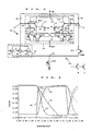
- Fig.1 shows a typical dual phase SCFL circuit implementation as it may be constructed from the above cited prior art.
- the circuit or gate referenced 10 basically consists of a differential amplifier DA and of two source follower output buffers OB11 and OB12.
- the differential amplifier forms a tree comprised of two branches coupled intermediate a current source at node 11 and a first supply voltage VH at node 12.
- the current source is formed by FET T10, with its gate and source shorted to function as a linear load over the operating range of circuit 10, coupled to a second supply voltage VD.
- the first branch comprises FET T11, the gate electrode of which is connected to a reference voltage VREF, connected in series with resistor R2.
- the other branch comprises FET T12 connected in series with resistor R1.
- a logic input signal E1 is applied on the input terminal I1 of FET T12.
- the other end of resistors R1 and R2 is coupled to said first supply voltage VH at node 12.
- Circuit 10 pertains to the SCFL technology because the source regions of FETs T11 and T12 are coupled together at node 11.
- FETs T11 and T12 operate as current switches.
- First and second output signals S1 and S2 of the differential amplifier are available at nodes 13 and 14 respectively intermediate said resistors and said current switches.
- Said nodes 13 and 14 are respectively connected to the inputs of two source follower output buffers OB11 and OB12 mounted in parallel between third and fourth supply voltages.
- the first source follower output buffer OB1 comprises active FET T13 loaded by resistively mounted FET T14. Generally speaking, shorted source-gate FETs are preferable to resistors.
- the second source follower output buffer OB2 comprises FETs T15 and T16. Inputs of said source follower output buffers are the gate electrodes of active FETs T13 and T15. The combination of the two source-follower output buffers forms output circuit block 16.
- circuit 10 operates as an inverter on one circuit output terminal.
- logic functions F more complex than INVERT are usually required, additional transistors have to be connected to FET T12, in parallel and/or in series. For example, adding two FETs, T17 and T18 mounted in parallel with FET T12 and respectively driven by logic input signals E2 and E3, forms a logic block referenced 19 which implements a 3 Way OR/NOR function in circuit 10.
- Fig. 1 The circuit of Fig. 1 has been shown implemented with FETs of the N type with both enhancement (E) and depletion (D) devices.
- SCFL circuits may be designed in various fashions, combining a differential amplifier structure supplying two complementary and simultaneous output logic signals (referred to as S1 and S2), with a pair of source follower output buffer stages respectively driven by said output logic signals, is a common practice to all versions of SCFL circuits of the prior art (see Fig. 2 of Refs. 2 and 3, for instance).
- each source follower output buffer may be understood as being comprised of an active pull up device (e.g. T13) and a passive pull down device (e.g. T14) connected in series.
- the latter device acts as a passive load.
- the active pull up devices T13 and T15 are loaded with important line capacitances (including wiring and fan-out capacitances) represented by C1 and C2 at circuit output terminals 17 and 18 respectively. Both capacitances C1 and C2 are connected to a reference potential, which in the present case is the ground potential or GND.
- capacitances C1 and C2 which are used for simulating circuit 10 are selected in the range extending from 0,1 to 4 pF.
- adjusting transistor sizes and resistor values is important to fix operating voltage levels and swings.
- the size of FET T10 and values of resistors R1 and R2 are determining parameters in that respect. For a given standard GaAs MESFET technology, typical parameters are given below in TABLE I.
- circuit of Fig. 1 is perfectly compatible with ECL logic levels, the supply voltages, levels of both input and circuit output signals being identical.
- SCFL logic technology is widely used, because it provides very fast switching. It is also nearly independent of the threshold voltages of the FETs since the critical level of the transfer characteristics is equal to the externally applied reference voltage VREF. SCFL circuits are particularly attractive when metal-semiconductor FETs (MESFETs) are employed with a GaAs substrate.
- MESFETs metal-semiconductor FETs
- SCFL circuits When built with high enough transconductance devices, such as short channel GaAs MESFETs, SCFL circuits can provide better speed capabilities than their bipolar counterparts but they suffer from the same disadvantage of high power consumption.
- each source follower output buffer e.g. OB11
- a passive pull down device typically a FET (e.g. T14) operating as an equivalent resistor R.
- This FET has to be a big device to have a small resistance, so that in AC conditions, capacitance e.g. C1 can discharge fast therein at down going transition of the signal.
- the active pull up device e.g. T13 is also a big device so that capacitance C1 is rapidly charged during up going transitions.
- the output down level exhibits a poor definition.
- Each push pull output buffer comprises an active pull up device connected in series with an active pull down device. Both pull up and pull down devices are controlled by said output signals which are substantially simultaneous and complementary to each other.
- a logice circuit according to the teachings of the present invention, say including output buffers with a push pull configuration.
- the novel circuit referenced 20 and so called PPSCFL is derived from the typical dual phase SCFL circuit 10 shown in Fig. 1. Same elements bear same references. It must be kept in mind that output logic block 16 is coupled between third and fourth supply voltages respectively at nodes 12 and 15. In the implementation of Fig. 2, third supply voltage is identical to said first supply voltage say VH. Circuit 20 features the addition of new devices.
- New devices consist first of active pull down FETs T20 and T21 that have been added in parallel to the passive loads, respectively FETs T14 and T16, of the source-follower output buffers OB11 and OB12 of Fig. 1. It is key to the present invention that for each output buffer so modified, the control signal applied to the gate electrode of the active pull down FET, be complementary and substantially simultaneous to the signal applied on the gate electrode of the corresponding active pull up FET. In other words, output buffers of circuit 20 are no longer of the source follower type but of the push pull type. First and second push pull output buffers are referenced PP21 and PP22 in Fig. 2. First and second circuit output signals A1 and B1 are available at respective output terminals 21 and 22.
- both polarities of the output signals of the differential amplifier say IN PHASE and OUT OF PHASE signals are available on the outputs of the tree that performs the logic function F. These signals are also simultaneous, with no skew there between.
- the differential amplifier like structure is therefore excellent candidate as a logic block to supply complementary and simultaneous output signals to the push pull output buffers.
- Other determining logic blocks such as latches, ... are also appropriate.
- the gate electrode of active pull up FET T13 is driven by first output signals S1, thus the gate electrode of active pull down FET T20 should be driven by the second output signal S2 available on the opposite side of the tree at node 14 or by a signal desired without delay and in phase with it.
- Symmetrical reasoning applies to pull down FET T21 in the second output buffer PP22. It is therefore important to generate the appropriate IN PHASE and OUT OF PHASE signals in terms of levels and with no noticeable delay therebetween.
- two additional buffer stages so called intermediate buffers IB21 and IB22 have been introduced between the differential amplifier output nodes 13 and 14, and the push pull output buffer stages PP21 and PP2.
- the first intermediate buffer stage IB1 consists of an active FET T22 loaded with a passive FET T23 connected in a source follower configuration.
- the second additional buffer stage comprised of FETs T24 and T25 is of similar structure. Active pull up FETs of buffers IB21 and PP21 on the one hand and IB22 and PP22 on the other hand are controlled by the same signal respectively S1 and S2. Signals A2 and B2 respectively available at intermediate output nodes 23 and 24 are appropriate for use, because they are in phase signals with S1 and S2 respectively. Due to the source follower structure of IB21 and IB22, A2 and B2 have appropriate voltage levels and are not delayed compared to original signals S1 and S2.
- signal B2 available at node 24 can drive the gate electrode of active pull down FET 20 of output buffer PP21, while the corresponding active pull up FET T13 is driven by S1.
- the major advantage of having introduced said intermediate buffer stages is to avoid the transitions at nodes 23 and 24 from being slowed down by the capacitive loads C1 and C2 at the output terminals 21 and 22. They have also the great advantage to switch simultaneously with their paired output buffer stage, so that a real push pull effect is obtained in the latter. Dual push pull operation results from the typical cross coupling of interconnections, as clear from Fig. 2.
- pull down devices either of the passive type, FETs T14, T16, T23, T25 and of the active type T20 and T21 are connected to said fourth supply voltage, which is no longer the supply VD, but the potential of the ground GND.
- This mere change has a significant impact as to decreasing the power dissipation also it accelerates the discharge of capacitive loads.
- the purpose of keeping FETs T14 and T16 in the circuit implementation is only to guarantee some current on T13 and T15 at the up level and to provide a better definition of this up level. If some degradation in performances is accepted, FETs T14 and T16 may be removed.
- First and second circuit logic output signals A1 and B1, complementary to each other, are respectively available at output nodes 21 and 22.
- the DC current in FETs T13 and T15 are therefore much smaller than in their counterparts of the conventional circuit shown in Fig. 1. All the transient currents necessary to pull down the output terminals 21 and 22 are supplied by devices T20 and T21. Even keeping passive FETs T14 and T16, the DC power consumption is drastically reduced.
- An intermediate buffer driven by the OUT OF PHASE signal is used to supply the control signal preferably to an inverter driven by the IN PHASE signal, to supply the complementary signal. This is because an inverter would introduce non desirable extra delay. However, if heavily degraded performances are accepted, they would be used as well. In this case a differential amplifier like structure supplying two logic output signals S1 and S2, complementary each other, is no longer necessary. A determining logic block supplying a single output logic signal is appropriate.
- a differential amplifier like structure as a determining logic block DA is recommended in the SCFL technology to supply two logic signals simultaneous and complementary each other.
- other logic blocks supplying complementary output signals such as latches, could be appropriate as well.
- implementing the present invention in whatever logic circuit including output buffers does not raise any difficulty, it is only necessary to have the determining logic block generating the appropriate IN PHASE and OUT OF PHASE signals for adequate push pull operation.
- the dual phase PPSCFL circuit 20 of Fig. 2 still implements a 3 Way OR/NOR logic function with NFETs.
- the type of FETs used to implement this circuit may be easily deduced from Fig. 2.
- terminal 22 is strongly pulled down by FET T21 while terminal 21 is strongly pulled up by FET T13.
- Fig.3 shows typical waveforms of the 3 Way OR/NOR circuit or gate shown in Fig. 2, when a pulse (logic input signal E1) represented by curve 30, is applied to the gate electrode of FET T12 at time t0, while inputs logic signals E2 and E3 are at a low level.
- the potentials at output terminals 21 and 21, say the circuit output signals A1 and B1, are represented by curves 31 and 32 respectively. It is clear from Fig. 3 that circuit output signals A1 and B1 are fairly symmetric each other with respect to a value of 0,35 V.
- a pulse is applied on the gate electrode of FET T12 while gate electrodes of FETs T17 and T18 are maintained at a low level.
- the logic input signal E1 is represented by curve 40.
- Waveforms at output nodes 16 and 17 of the conventional SCFL circuit is respectively represented by curves 41 and 42.
- Waveforms at output terminals 21 and 22 of the PPSCFL circuit of the present invention are represented by curves 43 and 44.
- the PPSCFL circuit exhibits more acute and balanced up going and down going transitions when compared to the standard SCFLL circuit.
- Circuit 20 totally eliminates the various inconveniences of the prior art circuit referenced 10 in Fig. 1. It takes advantage of the fact that both polarities of the signal are available on the outputs of the differential amplifier at nodes 13 and 14 to perform the logic function. As a result of the push pull configuration, cross-coupling the signals as shown in Fig.2, allows to switch on and off the output sink currents on each output. Implementing a push pull stage, therefore allows the reduction the power dissipation when compared with conventional SCFL circuits and the balance of the down-going transition with the up-going transition. In addition, it allows a better definition of the output down level since it is forced to ground by a transistor strongly turned on instead of being defined by a current through the load resistors (R1 or R2) of the differential amplifier of circuit 10 of Fig. 1.
- Output buffer PP21 has the gate electrode of its active pull down FET T20 driven by signal B2 which is in phase with signal S2. Same reasoning applies on the other branch for circuit output signal B1.
- FIG. 6 shows the modified circuit.
- the intermediate buffer stage IB22 comprised of FETs T24 and T25 is eliminated while still maintaining the adequate voltage levels on the gate electrode of T20. Same reasoning applies on the other branch for circuit output signal B1
- circuits of the family have some drawbacks.
- one to three additional devices per output are necessary to implement the invention.
- three devices T20, T22 and T23 are necessary to supply output signals A1 and A2.
- FETs T22 and T23 are really small devices but FET T20 may need to be large if the loading value at output terminal 21 is large, (note in that case, the power saving is even bigger).
- Time delays (in nanoseconds versus load capacitances in picofarads ranging from 0.3 to 4 pF) are shown in Fig. 7, for the single phase push pull circuit version (of the type shown in Fig. 5) using device models corresponding to a conventional Gallium Arsenide technology.
- Delay curves representing Tfall and Trise are respectively identified by references 70 and 71, for the conventional SCFL circuit of Fig. 1, and 72 and 73 for the single phase PPSCFL circuit of the present invention.
- Tfall of the regular SCFL is about two times longer than Trise (see curve 71), while the PPSCFL has a fall time well balanced with the fast rise time.
- Trise (curve 73) and Tfall (curve 72) of the PPSCFL circuit are even better than Trise (curve 71) of the SCFL circuit.
- the improvement is by a factor of 2 or 3 for capacitive loads larger than 1,5 pF.
- the concept at the base of the present invention may find extensive applications in the field of Ultra High Speed Integrated Circuits (UHSICs) especially when outputs are heavily loaded.
- UHSICs Ultra High Speed Integrated Circuits
- OR/NOR logic gates as referred to in the present application. But he invention is not limited thereto.
- Other potential applications include inverting and non inverting buffers, clock distribution, off-chip drivers, line drivers, ...etc.
- ASTAP simulations reported above were performed using a GaAs technology to take full advantage of it, in terms of speed and power consumption.
- principles of the present invention can be extended to silicon FETs, provided that the device dimensions are adjusted according to the technology characteristics. The better the transconductance and cutoff frequency, the better the circuit performance.
- FETs includes MESFETs, metal-oxide semiconductor FETs (MOSFETs), junction FETs (JFETs), modulation doped FETs (MODFETs) and any enhancement or depletion mode configurations of the same.
- circuit of Fig. 2 has been shown with N type MESFETs. Those skilled in the art will recognize that this circuit and others derived therefrom can be readily modified to employ other FETs, P type FETs and opposite power supplies. It is a popular configuration to use enhancement mode MESFETs as logic elements with depletion mode MESFETs as load elements as represented in Fig. 2. The circuits have been described in terms of positive logic but they are readily adapted to negative logic. GaAs is the preferred substrate material of the present invention, however other semiconductor materials and more particularly silicon as mentioned above, can be employed as well.
Landscapes
- Engineering & Computer Science (AREA)
- Physics & Mathematics (AREA)
- Computer Hardware Design (AREA)
- Computing Systems (AREA)
- General Engineering & Computer Science (AREA)
- Mathematical Physics (AREA)
- Power Engineering (AREA)
- Logic Circuits (AREA)
- Manipulation Of Pulses (AREA)
- Junction Field-Effect Transistors (AREA)
Priority Applications (4)
| Application Number | Priority Date | Filing Date | Title |
|---|---|---|---|
| EP88480011A EP0339165B1 (fr) | 1988-04-29 | 1988-04-29 | Circuits logiques mesfet GaAs comportant des tampons de sortie du type push-pull |
| DE3854155T DE3854155T2 (de) | 1988-04-29 | 1988-04-29 | GaAs-Mesfet-Logik-Schaltungen mit Gegentakt-Ausgangspufferschaltungen. |
| US07/271,124 US4922135A (en) | 1988-04-29 | 1988-11-14 | GaAs MESFET logic circuits including push pull output buffers |
| JP1066427A JP2534346B2 (ja) | 1988-04-29 | 1989-03-20 | 高速論理回路 |
Applications Claiming Priority (1)
| Application Number | Priority Date | Filing Date | Title |
|---|---|---|---|
| EP88480011A EP0339165B1 (fr) | 1988-04-29 | 1988-04-29 | Circuits logiques mesfet GaAs comportant des tampons de sortie du type push-pull |
Publications (2)
| Publication Number | Publication Date |
|---|---|
| EP0339165A1 true EP0339165A1 (fr) | 1989-11-02 |
| EP0339165B1 EP0339165B1 (fr) | 1995-07-12 |
Family
ID=8200492
Family Applications (1)
| Application Number | Title | Priority Date | Filing Date |
|---|---|---|---|
| EP88480011A Expired - Lifetime EP0339165B1 (fr) | 1988-04-29 | 1988-04-29 | Circuits logiques mesfet GaAs comportant des tampons de sortie du type push-pull |
Country Status (4)
| Country | Link |
|---|---|
| US (1) | US4922135A (fr) |
| EP (1) | EP0339165B1 (fr) |
| JP (1) | JP2534346B2 (fr) |
| DE (1) | DE3854155T2 (fr) |
Families Citing this family (9)
| Publication number | Priority date | Publication date | Assignee | Title |
|---|---|---|---|---|
| US5182473A (en) * | 1990-07-31 | 1993-01-26 | Cray Research, Inc. | Emitter emitter logic (EEL) and emitter collector dotted logic (ECDL) families |
| US5703519A (en) * | 1996-01-30 | 1997-12-30 | Analog Devices, Inc. | Drive circuit and method for controlling the cross point levels of a differential CMOS switch drive signal |
| KR100282432B1 (ko) * | 1998-08-31 | 2001-02-15 | 김영환 | 티디디비(tddb) 테스트 패턴 및 그를 이용한 모스캐패시터유전체막의 tddb테스트방법 |
| US6215330B1 (en) | 1999-06-11 | 2001-04-10 | Trw Inc. | Differential diode transistor logic (DDTL) circuit enhancements |
| US8027942B2 (en) * | 2000-12-13 | 2011-09-27 | International Business Machines Corporation | Method and circuits for associating a complex operator to each component of an input pattern presented to an artificial neural network |
| JP4159553B2 (ja) * | 2005-01-19 | 2008-10-01 | エルピーダメモリ株式会社 | 半導体装置の出力回路及びこれを備える半導体装置、並びに、出力回路の特性調整方法 |
| JP5257512B2 (ja) * | 2009-04-30 | 2013-08-07 | トヨタ自動車株式会社 | オイルパン |
| US9325318B1 (en) * | 2014-11-26 | 2016-04-26 | Taiwan Semiconductor Manufacturing Company Ltd. | Post driver |
| CN111682866B (zh) * | 2020-06-24 | 2024-02-09 | 天津中科海高微波技术有限公司 | 输出电流可调的GaAs开关驱动电路 |
Citations (6)
| Publication number | Priority date | Publication date | Assignee | Title |
|---|---|---|---|---|
| US4064405A (en) * | 1976-11-09 | 1977-12-20 | Westinghouse Electric Corporation | Complementary MOS logic circuit |
| US4450371A (en) * | 1982-03-18 | 1984-05-22 | Rca Corporation | Speed up circuit |
| US4496856A (en) * | 1982-07-21 | 1985-01-29 | Sperry Corporation | GaAs to ECL level converter |
| EP0215280A1 (fr) * | 1985-08-09 | 1987-03-25 | Siemens Aktiengesellschaft | Circuit de conversion de signaux |
| EP0237094A1 (fr) * | 1986-02-18 | 1987-09-16 | Laboratoires D'electronique Philips | Dispositif semi-conducteur du type réseau de portes prédiffusé pour circuits à la demande |
| EP0249287A1 (fr) * | 1986-06-10 | 1987-12-16 | Laboratoires D'electronique Philips | Circuit amplificateur différentiel régénérateur de signeaux complémentaires de faible amplitude |
Family Cites Families (6)
| Publication number | Priority date | Publication date | Assignee | Title |
|---|---|---|---|---|
| US4467455A (en) * | 1982-11-01 | 1984-08-21 | Motorola, Inc. | Buffer circuit |
| US4728821A (en) * | 1985-04-19 | 1988-03-01 | Digital Equipment Corporation | Source follower current mode logic cells |
| JPS62195915A (ja) * | 1986-02-24 | 1987-08-29 | Rohm Co Ltd | スイツチング回路 |
| JPS635553A (ja) * | 1986-06-25 | 1988-01-11 | Fujitsu Ltd | バツフア回路 |
| US4746817A (en) * | 1987-03-16 | 1988-05-24 | International Business Machines Corporation | BIFET logic circuit |
| US4831284A (en) * | 1988-03-22 | 1989-05-16 | International Business Machines Corporation | Two level differential current switch MESFET logic |
-
1988
- 1988-04-29 DE DE3854155T patent/DE3854155T2/de not_active Expired - Fee Related
- 1988-04-29 EP EP88480011A patent/EP0339165B1/fr not_active Expired - Lifetime
- 1988-11-14 US US07/271,124 patent/US4922135A/en not_active Expired - Fee Related
-
1989
- 1989-03-20 JP JP1066427A patent/JP2534346B2/ja not_active Expired - Lifetime
Patent Citations (6)
| Publication number | Priority date | Publication date | Assignee | Title |
|---|---|---|---|---|
| US4064405A (en) * | 1976-11-09 | 1977-12-20 | Westinghouse Electric Corporation | Complementary MOS logic circuit |
| US4450371A (en) * | 1982-03-18 | 1984-05-22 | Rca Corporation | Speed up circuit |
| US4496856A (en) * | 1982-07-21 | 1985-01-29 | Sperry Corporation | GaAs to ECL level converter |
| EP0215280A1 (fr) * | 1985-08-09 | 1987-03-25 | Siemens Aktiengesellschaft | Circuit de conversion de signaux |
| EP0237094A1 (fr) * | 1986-02-18 | 1987-09-16 | Laboratoires D'electronique Philips | Dispositif semi-conducteur du type réseau de portes prédiffusé pour circuits à la demande |
| EP0249287A1 (fr) * | 1986-06-10 | 1987-12-16 | Laboratoires D'electronique Philips | Circuit amplificateur différentiel régénérateur de signeaux complémentaires de faible amplitude |
Also Published As
| Publication number | Publication date |
|---|---|
| US4922135A (en) | 1990-05-01 |
| EP0339165B1 (fr) | 1995-07-12 |
| JPH0216811A (ja) | 1990-01-19 |
| DE3854155T2 (de) | 1996-02-29 |
| JP2534346B2 (ja) | 1996-09-11 |
| DE3854155D1 (de) | 1995-08-17 |
Similar Documents
| Publication | Publication Date | Title |
|---|---|---|
| CA1206535A (fr) | Circuit d'interface | |
| US7215169B2 (en) | Current-controlled CMOS logic family | |
| EP0493873B1 (fr) | Circuit tampon de sortie CMOS avec réduction des transitoires dans les lignes de masse | |
| US4777389A (en) | Output buffer circuits for reducing ground bounce noise | |
| US4695744A (en) | Level shift circuit including source follower output | |
| US4638187A (en) | CMOS output buffer providing high drive current with minimum output signal distortion | |
| US6982583B2 (en) | Current-controlled CMOS circuit using higher voltage supply in low voltage CMOS process | |
| US4437024A (en) | Actively controlled input buffer | |
| US4831284A (en) | Two level differential current switch MESFET logic | |
| US4724342A (en) | Push-pull DCFL driver circuit | |
| US4798972A (en) | Apparatus and method for capacitor coupled complementary buffering | |
| US4406957A (en) | Input buffer circuit | |
| US4922135A (en) | GaAs MESFET logic circuits including push pull output buffers | |
| US5045721A (en) | Zero static current high speed TTL compatible buffer | |
| US5541528A (en) | CMOS buffer circuit having increased speed | |
| JPH02149123A (ja) | 増幅回路 | |
| US4954730A (en) | Complementary FET circuit having merged enhancement/depletion FET output | |
| US6215330B1 (en) | Differential diode transistor logic (DDTL) circuit enhancements | |
| KR950000352B1 (ko) | 반도체 논리회로 | |
| EP0655177A1 (fr) | Traducteur de niveau ecl a cmos d'un bicmos et tampon | |
| US6124734A (en) | High-speed push-pull output stage for logic circuits | |
| JPH07264049A (ja) | 論理ゲート | |
| JPH01133415A (ja) | トランジスタ・スイッチング回路 | |
| JPH01296814A (ja) | 半導体集積回路 | |
| JPH08250998A (ja) | 出力バッファ回路 |
Legal Events
| Date | Code | Title | Description |
|---|---|---|---|
| PUAI | Public reference made under article 153(3) epc to a published international application that has entered the european phase |
Free format text: ORIGINAL CODE: 0009012 |
|
| AK | Designated contracting states |
Kind code of ref document: A1 Designated state(s): DE FR GB |
|
| 17P | Request for examination filed |
Effective date: 19900224 |
|
| 17Q | First examination report despatched |
Effective date: 19910617 |
|
| GRAA | (expected) grant |
Free format text: ORIGINAL CODE: 0009210 |
|
| AK | Designated contracting states |
Kind code of ref document: B1 Designated state(s): DE FR GB |
|
| ET | Fr: translation filed | ||
| REF | Corresponds to: |
Ref document number: 3854155 Country of ref document: DE Date of ref document: 19950817 |
|
| PGFP | Annual fee paid to national office [announced via postgrant information from national office to epo] |
Ref country code: FR Payment date: 19960412 Year of fee payment: 9 |
|
| PG25 | Lapsed in a contracting state [announced via postgrant information from national office to epo] |
Ref country code: GB Effective date: 19960429 |
|
| PLBE | No opposition filed within time limit |
Free format text: ORIGINAL CODE: 0009261 |
|
| STAA | Information on the status of an ep patent application or granted ep patent |
Free format text: STATUS: NO OPPOSITION FILED WITHIN TIME LIMIT |
|
| 26N | No opposition filed | ||
| GBPC | Gb: european patent ceased through non-payment of renewal fee |
Effective date: 19960429 |
|
| PG25 | Lapsed in a contracting state [announced via postgrant information from national office to epo] |
Ref country code: DE Effective date: 19970101 |
|
| PG25 | Lapsed in a contracting state [announced via postgrant information from national office to epo] |
Ref country code: FR Free format text: LAPSE BECAUSE OF NON-PAYMENT OF DUE FEES Effective date: 19971231 |
|
| REG | Reference to a national code |
Ref country code: FR Ref legal event code: ST |
|
| APAH | Appeal reference modified |
Free format text: ORIGINAL CODE: EPIDOSCREFNO |