EP0339738B1 - Circuit diviseur de courant - Google Patents
Circuit diviseur de courant Download PDFInfo
- Publication number
- EP0339738B1 EP0339738B1 EP89201054A EP89201054A EP0339738B1 EP 0339738 B1 EP0339738 B1 EP 0339738B1 EP 89201054 A EP89201054 A EP 89201054A EP 89201054 A EP89201054 A EP 89201054A EP 0339738 B1 EP0339738 B1 EP 0339738B1
- Authority
- EP
- European Patent Office
- Prior art keywords
- current
- paths
- circuit
- node
- similar
- Prior art date
- Legal status (The legal status is an assumption and is not a legal conclusion. Google has not performed a legal analysis and makes no representation as to the accuracy of the status listed.)
- Expired - Lifetime
Links
Images
Classifications
-
- G—PHYSICS
- G05—CONTROLLING; REGULATING
- G05F—SYSTEMS FOR REGULATING ELECTRIC OR MAGNETIC VARIABLES
- G05F3/00—Non-retroactive systems for regulating electric variables by using an uncontrolled element, or an uncontrolled combination of elements, such element or such combination having self-regulating properties
- G05F3/02—Regulating voltage or current
- G05F3/08—Regulating voltage or current wherein the variable is DC
- G05F3/10—Regulating voltage or current wherein the variable is DC using uncontrolled devices with non-linear characteristics
- G05F3/16—Regulating voltage or current wherein the variable is DC using uncontrolled devices with non-linear characteristics being semiconductor devices
- G05F3/20—Regulating voltage or current wherein the variable is DC using uncontrolled devices with non-linear characteristics being semiconductor devices using diode- transistor combinations
- G05F3/22—Regulating voltage or current wherein the variable is DC using uncontrolled devices with non-linear characteristics being semiconductor devices using diode- transistor combinations wherein the transistors are of the bipolar type only
-
- G—PHYSICS
- G05—CONTROLLING; REGULATING
- G05F—SYSTEMS FOR REGULATING ELECTRIC OR MAGNETIC VARIABLES
- G05F3/00—Non-retroactive systems for regulating electric variables by using an uncontrolled element, or an uncontrolled combination of elements, such element or such combination having self-regulating properties
- G05F3/02—Regulating voltage or current
- G05F3/08—Regulating voltage or current wherein the variable is DC
- G05F3/10—Regulating voltage or current wherein the variable is DC using uncontrolled devices with non-linear characteristics
- G05F3/16—Regulating voltage or current wherein the variable is DC using uncontrolled devices with non-linear characteristics being semiconductor devices
- G05F3/20—Regulating voltage or current wherein the variable is DC using uncontrolled devices with non-linear characteristics being semiconductor devices using diode- transistor combinations
- G05F3/26—Current mirrors
- G05F3/262—Current mirrors using field-effect transistors only
Definitions
- the invention relates to a current divider circuit for receiving at a node a signal current and dividing the signal current in predetermined proportions between a plurality of current paths.
- signal current refers to any current whose purpose includes conveying information of some sort, in contradistinction, for example, to a mere supply current.
- each path usually comprises a transistor and the transistors of all the paths are designed to be identical or 'similar', meaning that the currents flowing through the different transistors are equal or are related in accordance with ratios defined by the relative geometries of the transistors.
- the transistors may be bipolar (or MOS) types, with the emitter (or source) of each transistor connected to the input node and the base (or gate) of each transistor being connected to a common bias point.
- These circuits operate according to the well-known 'current-mirror' principle.
- the invention provides a current divider circuit for receiving at a node a signal current and dividing the signal current in predetermined proportions between a plurality of current paths, characterised in that the current paths include one or more first current paths formed by a first type of impedance element and one or more second current paths formed by a type or types of impedance element dissimilar to the first type, each second current path including an output branch of a current mirror circuit, the input branch of each such current mirror circuit being connected to the node via a further current path formed by the first type of impedance element.
- the further current path(s) and current mirror circuit(s) ensures that a predetermined proportion of the signal current can be made to flow into each current path, even though the second current path(s) may contain arbitrary or unknown impedances.
- Each second current path may have its own separate further current path and current mirror circuit. This may be favourable if the proportions of the total current flowing in different second current paths differ widely.
- the current divider circuit may have a single further current path and a plurality of second current paths wherein the further current path is connected to the input branch of a current mirror circuit having a corresponding plurality of output branches. This is not only economical of components, but also reduces the additional load imposed by the further current path(s) on whatever is the source of the signal current.
- the first current path(s) and the further current path(s) may comprise the main current paths of similar transistors having control electrodes connected to a common bias voltage so that relative geometries of the transistors define the said predetermined proportions.
- Such an embodiment can conveniently be formed by integration, whereby the transistors can be made to be accurately similar, since they are all produced by the same manufacturing process on the same semiconductor substrate.
- Each similar transistor may be a metal-oxide-semiconductor field-effect transistor (MOSFET), the source-drain paths of the MOSFETs forming the paths of similar impedance, the source electrodes of the MOSFETs being connected to the node, the gate electrodes of the MOSFETs being connected to the common bias voltage, and the aspect ratios (W/L) of the similar MOSFETs defining the said predetermined proportions.
- the aspect ratio (W/L) of a field-effect transistor is the ratio of the width W of its channel to the length L of its channel, both being expressed in micrometres, for example.
- the geometry of the channels of MOS transistors can be scaled conveniently to give the desired ratios between the currents in the various paths, either by actually altering the length (L) and/or width (W) of the channel or simply by connecting a number of identical unit transistors in parallel (the effective aspect ratio of N identical transistors in parallel equals N times the aspect ratio of one such transistor).
- the latter approach avoids the problem that errors due to "end-effects" are different in different-sized transistors.
- the invention further provides a circuit comprising a current divider circuit as described in either of the last two preceding paragraphs, and further comprising means for varying the common bias voltage, thereby to vary the voltage at the node while maintaining the predetermined proportions of the divided signal current.
- the circuit allows control of the voltage while simultaneously giving access to accurately defined portions of the signal current, which may be used, for example for measuring the signal current or for passing through any desired impedance network, be it fixed, variable, inductive, capacitive or whatever.
- controlling the voltage at the node may, indirectly, also affect the signal current.
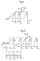
- Figure 1 shows a conventional p-channel current mirror divider circuit which receives a current I via an input 10 which is connected to a node 12.
- the circuit divides the current I into a number N of smaller currents I1 to I N flowing through N paths which include similar impedances and leave the circuit through respective outputs 14-1 to 14-N.
- "similar" impedances are to be taken to be impedances which are related so that if placed under identical bias conditions each will pass the same current, or a current related by a fixed ratio to the other currents.
- Such similar impedances will be formed by active devices, integrated close to one another on a common substrate so as to be as closely matched as possible.
- the currents I1 to I N flow through respective p-channel MOS transistors T1 to TN.
- the sources of the transistors T1 to TN are all connected to the node 12 and the gates of the transistors T1 to TN are all connected to a bias input 16 so that the transistors T1 to TN all have the same gate-source voltage applied to them.
- the well-known current-mirror principle ensures that the division of the current I into the smaller currents I1 to I N occurs in proportions predetermined by the relative geometries of the transistors T1 to TN.
- the proportion of the total current I n flowing in each output 14-n will depend on the aspect ratios (W/L)1 to (W/L) N of the transistors T1 to TN in accordance with the Formula (1) below.
- DAC digital-to-analogue converter
- the DAC will further comprise switching circuits so that each current I n , which corresponds to a bit position in the digital input signal can be added into the analogue output signal or not, depending on the value of the corresponding bit in the actual input signal.
- FIG. 2 shows a current divider circuit in accordance with the present invention.
- the total current I enters the circuit via an input 20 which is connected to a node 22.
- Smaller currents I1′ to I N ′ leave the node 22 to flow through N first current paths to N outputs 24-1 to 24-N respectively.
- the first current paths are formed by N similar impedance elements which in this embodiment are similar p-channel MOS transistors T1′ to TN′ as in Figure 1.
- the sources of the transistors T1′ to TN′ are connected to the node 22 and the gates of the transistors T1′ to TN′ are connected to a bias input 26 to which is applied a suitable bias voltage V BIAS .
- Each transistor T1′ to TN′ has an associated aspect ratio (W/L)1′ to (W/L) N ′.
- the element Z1 could be a MOSFET which is identical to the transistors T1′ to TN′ but which is supplied with different bias voltages; it could be a different type of transistor (for example n-channel, bipolar or high-voltage); or it could be a diode, resistor, capacitor, inductor, thermistor or a totally unknown impedance network.
- a further current path 30 is provided which is formed by an impedance element of the first type, namely a further p-channel transistor T0′ similar to the transistors T1′ to TN′, the transistor T0′ having its source connected to the node 22 and its gate connected to the bias input 26.
- the further current path 28 terminates in the input of a current mirror circuit 32 which has an n-channel input transistor 34 and an n-channel output transistor 36-1.
- the n-channel transistors 34 and 36-1 are similar, with geometries scaled so as to define a ratio 1:X1 between the input current I0 flowing in the path 30 and the output current I Z1 flowing in the path 28.
- the further transistor T0′ generates the current I0′ in the path 30 in accordance with the current mirror principle so that the N+1 currents I0′ to I N ′ are related to one another by predetermined ratios corresponding to the aspect ratios of the (W/L)0′ to (W/L) N ′ of the p-channel transistors T0′ to TN′.
- the current mirror circuit 32 then ensures that the current I Z1 in the current path 28, which flows through the arbitrary impedance Z1, is related to current I0′ by a predetermined ratio X1:1 and is therefore also related to all the currents I1′ to I N ′ as well.
- the division of the total current I between the various current paths is effected in predetermined proportions, even though one of the current paths has an impedance Z1 totally unrelated to the impedances of the other paths.
- Formula (2) and Formula (3) below define the relationships between the currents in the circuit of Figure 2.
- Formula (2) differs from Formula (1) in that it is necessary to take into account all the currents flowing from the node 22, rather than just those flowing through the first current paths.
- I Z1 X1.I0' (3)
- a current divider circuit in accordance with the present invention has many possible applications, and many variations are possible to suit particular circumstances. For example, if it is necessary to pass a known fraction of the current I through more than one arbitrary impedance, for example the impedance Z1 and a further impedance Z2 (shown dotted in Figure 2), this can be done simply by providing a further output transistor 36-2 (shown dotted) in the current mirror circuit 32 .
- an additional arbitrary impedance (similar to Z2) could be provided for by means of a separate further p-channel transistor (similar to T0') and a separate n-channel current mirror circuit (similar to current mirror circuit 32 ). This might be favourable for example if it is required to give the additional impedance a much greater or smaller share of the total current than that given to the impedance Z1.
- the current mirror circuit 32 (or any separate current mirror circuit driven by a separate further transistor) can also be provided with a further output transistor 38 (shown dotted) which draws a current I Y from an output 40 via an impedance Y (also shown dotted).
- the current I Y will be related by a predetermined ratio to the currents I, I0' to I N ' and I Z1 to I ZM , but will not be a part of the total current I drawn from the node 22.
- the aspect ratio of a transistor such as transistor 38 should not be included in the (1 + X) term on the denominator of Formula (2). However, it is necessary to include a term corresponding to (W/L)0' for every further transistor provided, even if it drives only a separate current mirror circuit whose output current is not drawn from the node 22.
- a circuit such as that shown in Figure 2 in which N 2 and which includes the parts 38 and Y but excludes the parts 36-2 and Z2, is described in use in United Kingdom patent application No. 8810166.2 having the same priority date as the present application, now published as GB 2 217 938A. That application relates to a current sensing circuit of the type disclosed in EP-A1-227 149 for use with a cellular power semiconductor device.
- the input 10 of a current divider according to the present invention is connected to a representative cell of a many-celled power transistor.
- the divider circuit acts as a whole to control the voltage on the input 10 so that it is equal to the voltage on the remainder main portion of the power transistor, which includes a much larger number of cells.
- V CONT V BIAS
- the voltage V BIAS is a constant voltage which gives rise to a 'passive' divider circuit.
- the transistors T0' to TN' act to maintain the node 22 a threshold voltage above the control voltage V CONT and in the current sensing circuit, the bias input 26 is driven by the output of a differential amplifier to create a divider circuit which actively controls the voltage on the input as well as dividing the current I flowing into it.
- the terminal 40 is connected to the main portion of the power transistor and the impedance Y is a forward biased diode connected n-channel MOSFET, which provides a voltage level shifting function at the input to the differential amplifier.
- the divider circuit ensures that I1' and I2' are known fractions of the total current in the representative cell, and because the representative cell is maintained under the same bias as the major portion of the power transistor by the feedback action of the differential amplifier and the divider circuit, the currents I1 and I2 provide an accurate measure, on a very small scale, of the output current of the power transistor.
Landscapes
- Engineering & Computer Science (AREA)
- Microelectronics & Electronic Packaging (AREA)
- Physics & Mathematics (AREA)
- Nonlinear Science (AREA)
- Electromagnetism (AREA)
- General Physics & Mathematics (AREA)
- Radar, Positioning & Navigation (AREA)
- Automation & Control Theory (AREA)
- Amplifiers (AREA)
- Networks Using Active Elements (AREA)
- Analogue/Digital Conversion (AREA)
Claims (5)
- Circuit diviseur de courant pour la réception à un noeud d'un courant de signal et la division du courant de signal en proportions prédéterminées entre plusieurs trajets de courant, caractérisé en ce que les trajets de courant comprennent un ou plusieurs premiers trajets de courant formés par un élément d'impédance d'un premier type et un ou plusieurs deuxièmes trajets de courant formés par un élément d'impédance d'un type ou de types différents du premier type, chaque deuxième trajet de courant comportant une branche de sortie d'un circuit miroir de courant, la branche d'entrée de chaque circuit miroir de courant étant connectée au noeud par l'intermédiaire d'un autre trajet de courant formé par un élément d'impédance du premier type.
- Circuit diviseur de courant selon la revendication 1 dans lequel le (les) premier(s) trajet(s) de courant et l' (les) autre(s) trajet(s) de courant comprennent les trajets de courant principal de transistors analogues présentant des électrodes de commande connectées à une tension de polarisation commune de façon que les géométries relatives des transistors définissent les proportions prédéterminées.
- Circuit diviseur de courant selon la revendication 2, dans lequel chaque transistor analogue est un transistor à effet de champ métal-oxyde-semiconducteur (MOSFET), les trajets de source-drain des MOSFET constituant les trajets d'impédance analogue, les électrodes de source des MOSFET étant connectées au noeud, les électrodes de porte des MOSFET étant connectées à la tension de polarisation commune et les formats (W/L) des MOSFET analogues définissant lesdites proportions prédéterminées.
- Circuit diviseur de courant selon l'une des revendications précédentes, présentant un seul autre trajet de courant et plusieurs deuxièmes trajets de courant, dans lequel l'autre trajet de courant est connecté à la branche d'entrée d'un circuit miroir de courant présentant un nombre correspondant de branches de sortie.
- Circuit comprenant un circuit diviseur de courant selon l'une des revendications 2 à 4 et puis des moyens pour modifier la tension de polarisation commune de façon à modifier la tension au noeud, tout en maintenant les proportions prédéterminées du courant de signal divisé.
Applications Claiming Priority (2)
| Application Number | Priority Date | Filing Date | Title |
|---|---|---|---|
| GB8810163 | 1988-04-29 | ||
| GB8810163A GB2217937A (en) | 1988-04-29 | 1988-04-29 | Current divider circuit |
Publications (2)
| Publication Number | Publication Date |
|---|---|
| EP0339738A1 EP0339738A1 (fr) | 1989-11-02 |
| EP0339738B1 true EP0339738B1 (fr) | 1993-11-24 |
Family
ID=10636089
Family Applications (1)
| Application Number | Title | Priority Date | Filing Date |
|---|---|---|---|
| EP89201054A Expired - Lifetime EP0339738B1 (fr) | 1988-04-29 | 1989-04-24 | Circuit diviseur de courant |
Country Status (5)
| Country | Link |
|---|---|
| US (1) | US4973857A (fr) |
| EP (1) | EP0339738B1 (fr) |
| JP (1) | JPH01314429A (fr) |
| DE (1) | DE68910869T2 (fr) |
| GB (1) | GB2217937A (fr) |
Families Citing this family (9)
| Publication number | Priority date | Publication date | Assignee | Title |
|---|---|---|---|---|
| US5369309A (en) * | 1991-10-30 | 1994-11-29 | Harris Corporation | Analog-to-digital converter and method of fabrication |
| US5994755A (en) | 1991-10-30 | 1999-11-30 | Intersil Corporation | Analog-to-digital converter and method of fabrication |
| EP0555905B1 (fr) * | 1992-02-11 | 1996-12-18 | Koninklijke Philips Electronics N.V. | Diviseur de courant et circuit intégré muni de plusieurs diviseurs de courant |
| US6288602B1 (en) * | 1993-06-25 | 2001-09-11 | International Business Machines Corporation | CMOS on-chip precision voltage reference scheme |
| US6166590A (en) * | 1998-05-21 | 2000-12-26 | The University Of Rochester | Current mirror and/or divider circuits with dynamic current control which are useful in applications for providing series of reference currents, subtraction, summation and comparison |
| EP1676363B1 (fr) * | 2003-10-13 | 2009-08-26 | Nxp B.V. | Circuit de transconductance |
| TWI381266B (zh) * | 2008-08-28 | 2013-01-01 | Etron Technology Inc | 一種對於臨界電壓變異有免疫效果的電流源及其產生方法 |
| WO2011049994A2 (fr) * | 2009-10-20 | 2011-04-28 | Lam Research Corporation | Régulation du courant dans des systèmes de traitement plasma |
| US10590278B2 (en) | 2017-04-10 | 2020-03-17 | Nanophase Technologies Corporation | Coated powders having high photostability |
Family Cites Families (20)
| Publication number | Priority date | Publication date | Assignee | Title |
|---|---|---|---|---|
| NL169239C (nl) * | 1971-10-21 | 1982-06-16 | Philips Nv | Stroomversterker. |
| US4243948A (en) * | 1979-05-08 | 1981-01-06 | Rca Corporation | Substantially temperature-independent trimming of current flows |
| CA1152582A (fr) * | 1979-11-05 | 1983-08-23 | Takashi Okada | Circuit multiplicateur de courant |
| US4339729A (en) * | 1980-03-27 | 1982-07-13 | Motorola, Inc. | Analog integrated filter circuit |
| US4379267A (en) * | 1980-06-25 | 1983-04-05 | Mostek Corporation | Low power differential amplifier |
| JPS5714918A (en) * | 1980-07-02 | 1982-01-26 | Sony Corp | Constant current circuit |
| JPS596606A (ja) * | 1982-07-05 | 1984-01-13 | Yokogawa Hokushin Electric Corp | 比率演算方式 |
| JPS60107118A (ja) * | 1983-11-16 | 1985-06-12 | Nec Corp | 電圧電流変換回路 |
| IT1162859B (it) * | 1983-05-12 | 1987-04-01 | Cselt Centro Studi Lab Telecom | Circuito di polarizzazione per circuiti integrati bipolari multifunzione |
| US4525683A (en) * | 1983-12-05 | 1985-06-25 | Motorola, Inc. | Current mirror having base current error cancellation circuit |
| NL8400636A (nl) * | 1984-02-29 | 1985-09-16 | Philips Nv | Stroombronschakeling. |
| US4645948A (en) * | 1984-10-01 | 1987-02-24 | At&T Bell Laboratories | Field effect transistor current source |
| US4608530A (en) * | 1984-11-09 | 1986-08-26 | Harris Corporation | Programmable current mirror |
| JPS61226816A (ja) * | 1985-03-30 | 1986-10-08 | Toshiba Corp | 定電流源回路 |
| US4618816A (en) * | 1985-08-22 | 1986-10-21 | National Semiconductor Corporation | CMOS ΔVBE bias current generator |
| JPS62105508A (ja) * | 1985-10-31 | 1987-05-16 | Sharp Corp | 電流増幅回路 |
| NL8503394A (nl) * | 1985-12-10 | 1987-07-01 | Philips Nv | Stroomaftastschakeling voor een vermogenshalfgeleiderinrichting, in het bijzonder geintegreerde intelligente vermogenshalfgeleiderschakelaar voor met name automobieltoepassingen. |
| GB2186140B (en) * | 1986-01-30 | 1989-11-01 | Plessey Co Plc | Current source circuit |
| JPH0799802B2 (ja) * | 1986-03-19 | 1995-10-25 | ソニー株式会社 | レベルシフト回路 |
| US4717845A (en) * | 1987-01-02 | 1988-01-05 | Sgs Semiconductor Corporation | TTL compatible CMOS input circuit |
-
1988
- 1988-04-29 GB GB8810163A patent/GB2217937A/en not_active Withdrawn
-
1989
- 1989-04-07 US US07/334,961 patent/US4973857A/en not_active Expired - Fee Related
- 1989-04-24 DE DE68910869T patent/DE68910869T2/de not_active Expired - Fee Related
- 1989-04-24 EP EP89201054A patent/EP0339738B1/fr not_active Expired - Lifetime
- 1989-04-27 JP JP1106089A patent/JPH01314429A/ja active Pending
Also Published As
| Publication number | Publication date |
|---|---|
| DE68910869D1 (de) | 1994-01-05 |
| GB8810163D0 (en) | 1988-06-02 |
| DE68910869T2 (de) | 1994-05-19 |
| US4973857A (en) | 1990-11-27 |
| EP0339738A1 (fr) | 1989-11-02 |
| JPH01314429A (ja) | 1989-12-19 |
| GB2217937A (en) | 1989-11-01 |
Similar Documents
| Publication | Publication Date | Title |
|---|---|---|
| US6433624B1 (en) | Threshold voltage generation circuit | |
| US5440277A (en) | VCO bias circuit with low supply and temperature sensitivity | |
| US8692584B2 (en) | Semiconductor integrated circuit device | |
| EP0454250B1 (fr) | Générateur de référence | |
| US5900772A (en) | Bandgap reference circuit and method | |
| US4448549A (en) | Temperature sensing device | |
| EP0254212A2 (fr) | Circuit semi-conducteur MOS | |
| Kettner et al. | Analog CMOS realization of fuzzy logic membership functions | |
| US20030076159A1 (en) | Stack element circuit | |
| US20080180070A1 (en) | Reference voltage generation circuit | |
| EP0585755A1 (fr) | Circuit et procédé pour générer une tension de référence MOS compensée en température pour des applications à tension basse et des grandes plages de fonctionnement | |
| US20100244808A1 (en) | Method and circuit for low power voltage reference and bias current generator | |
| US7038482B1 (en) | Circuit and method for automatic measurement and compensation of transistor threshold voltage mismatch | |
| EP0339738B1 (fr) | Circuit diviseur de courant | |
| US4329639A (en) | Low voltage current mirror | |
| US9804629B1 (en) | Method and apparatus for current sensing and measurement | |
| JPH02117208A (ja) | 相補性mos技術による回路装置 | |
| US6586919B2 (en) | Voltage-current converter | |
| JP2001510609A (ja) | 温度補償された出力基準電圧を有する基準電圧源 | |
| WO1997030384A1 (fr) | Miroir de courant cmos | |
| US6340882B1 (en) | Accurate current source with an adjustable temperature dependence circuit | |
| EP0601750B1 (fr) | Circuit d'entrée pour un circuit intégré | |
| US4068140A (en) | MOS source follower circuit | |
| EP0762634A2 (fr) | Convertisseur tension-courant à résistance de référence MOS | |
| KR20030023476A (ko) | 반도체 장치 |
Legal Events
| Date | Code | Title | Description |
|---|---|---|---|
| PUAI | Public reference made under article 153(3) epc to a published international application that has entered the european phase |
Free format text: ORIGINAL CODE: 0009012 |
|
| AK | Designated contracting states |
Kind code of ref document: A1 Designated state(s): DE FR GB IT |
|
| 17P | Request for examination filed |
Effective date: 19900425 |
|
| RAP3 | Party data changed (applicant data changed or rights of an application transferred) |
Owner name: N.V. PHILIPS' GLOEILAMPENFABRIEKEN Owner name: PHILIPS ELECTRONICS UK LIMITED |
|
| 17Q | First examination report despatched |
Effective date: 19920824 |
|
| GRAA | (expected) grant |
Free format text: ORIGINAL CODE: 0009210 |
|
| AK | Designated contracting states |
Kind code of ref document: B1 Designated state(s): DE FR GB IT |
|
| REF | Corresponds to: |
Ref document number: 68910869 Country of ref document: DE Date of ref document: 19940105 |
|
| ITF | It: translation for a ep patent filed | ||
| ET | Fr: translation filed | ||
| ITTA | It: last paid annual fee | ||
| PLBE | No opposition filed within time limit |
Free format text: ORIGINAL CODE: 0009261 |
|
| STAA | Information on the status of an ep patent application or granted ep patent |
Free format text: STATUS: NO OPPOSITION FILED WITHIN TIME LIMIT |
|
| 26N | No opposition filed | ||
| ITPR | It: changes in ownership of a european patent |
Owner name: CAMBIO RAGIONE SOCIALE;PHILIPS ELECTRONICS N.V. |
|
| REG | Reference to a national code |
Ref country code: FR Ref legal event code: CD |
|
| PGFP | Annual fee paid to national office [announced via postgrant information from national office to epo] |
Ref country code: GB Payment date: 19970401 Year of fee payment: 9 |
|
| PGFP | Annual fee paid to national office [announced via postgrant information from national office to epo] |
Ref country code: FR Payment date: 19970422 Year of fee payment: 9 |
|
| PGFP | Annual fee paid to national office [announced via postgrant information from national office to epo] |
Ref country code: DE Payment date: 19970624 Year of fee payment: 9 |
|
| PG25 | Lapsed in a contracting state [announced via postgrant information from national office to epo] |
Ref country code: GB Free format text: LAPSE BECAUSE OF NON-PAYMENT OF DUE FEES Effective date: 19980424 |
|
| PG25 | Lapsed in a contracting state [announced via postgrant information from national office to epo] |
Ref country code: FR Free format text: THE PATENT HAS BEEN ANNULLED BY A DECISION OF A NATIONAL AUTHORITY Effective date: 19980430 |
|
| GBPC | Gb: european patent ceased through non-payment of renewal fee |
Effective date: 19980424 |
|
| PG25 | Lapsed in a contracting state [announced via postgrant information from national office to epo] |
Ref country code: DE Free format text: LAPSE BECAUSE OF NON-PAYMENT OF DUE FEES Effective date: 19990202 |
|
| REG | Reference to a national code |
Ref country code: FR Ref legal event code: ST |
|
| PG25 | Lapsed in a contracting state [announced via postgrant information from national office to epo] |
Ref country code: IT Free format text: LAPSE BECAUSE OF NON-PAYMENT OF DUE FEES Effective date: 20050424 |