EP0339794A1 - Tête d'impression par points à aiguilles - Google Patents
Tête d'impression par points à aiguilles Download PDFInfo
- Publication number
- EP0339794A1 EP0339794A1 EP89303034A EP89303034A EP0339794A1 EP 0339794 A1 EP0339794 A1 EP 0339794A1 EP 89303034 A EP89303034 A EP 89303034A EP 89303034 A EP89303034 A EP 89303034A EP 0339794 A1 EP0339794 A1 EP 0339794A1
- Authority
- EP
- European Patent Office
- Prior art keywords
- electromagnets
- wire
- coils
- conduction control
- current conduction
- Prior art date
- Legal status (The legal status is an assumption and is not a legal conclusion. Google has not performed a legal analysis and makes no representation as to the accuracy of the status listed.)
- Granted
Links
- 230000004907 flux Effects 0.000 claims description 15
- 230000002093 peripheral effect Effects 0.000 claims description 2
- 238000010586 diagram Methods 0.000 description 12
- BGPVFRJUHWVFKM-UHFFFAOYSA-N N1=C2C=CC=CC2=[N+]([O-])C1(CC1)CCC21N=C1C=CC=CC1=[N+]2[O-] Chemical compound N1=C2C=CC=CC2=[N+]([O-])C1(CC1)CCC21N=C1C=CC=CC1=[N+]2[O-] BGPVFRJUHWVFKM-UHFFFAOYSA-N 0.000 description 7
- 230000006698 induction Effects 0.000 description 6
- 239000002699 waste material Substances 0.000 description 3
- 230000000694 effects Effects 0.000 description 2
- 239000000470 constituent Substances 0.000 description 1
- 230000005284 excitation Effects 0.000 description 1
- 238000012986 modification Methods 0.000 description 1
- 230000004048 modification Effects 0.000 description 1
Images

Classifications
-
- B—PERFORMING OPERATIONS; TRANSPORTING
- B41—PRINTING; LINING MACHINES; TYPEWRITERS; STAMPS
- B41J—TYPEWRITERS; SELECTIVE PRINTING MECHANISMS, i.e. MECHANISMS PRINTING OTHERWISE THAN FROM A FORME; CORRECTION OF TYPOGRAPHICAL ERRORS
- B41J2/00—Typewriters or selective printing mechanisms characterised by the printing or marking process for which they are designed
- B41J2/22—Typewriters or selective printing mechanisms characterised by the printing or marking process for which they are designed characterised by selective application of impact or pressure on a printing material or impression-transfer material
- B41J2/23—Typewriters or selective printing mechanisms characterised by the printing or marking process for which they are designed characterised by selective application of impact or pressure on a printing material or impression-transfer material using print wires
- B41J2/235—Print head assemblies
- B41J2/25—Print wires
-
- B—PERFORMING OPERATIONS; TRANSPORTING
- B41—PRINTING; LINING MACHINES; TYPEWRITERS; STAMPS
- B41J—TYPEWRITERS; SELECTIVE PRINTING MECHANISMS, i.e. MECHANISMS PRINTING OTHERWISE THAN FROM A FORME; CORRECTION OF TYPOGRAPHICAL ERRORS
- B41J2/00—Typewriters or selective printing mechanisms characterised by the printing or marking process for which they are designed
- B41J2/22—Typewriters or selective printing mechanisms characterised by the printing or marking process for which they are designed characterised by selective application of impact or pressure on a printing material or impression-transfer material
- B41J2/23—Typewriters or selective printing mechanisms characterised by the printing or marking process for which they are designed characterised by selective application of impact or pressure on a printing material or impression-transfer material using print wires
- B41J2/30—Control circuits for actuators
Definitions
- the present invention relates to a wire-dot print head of the spring-charge type used in a serial printer, and more particularly to a spring-charge type wire-dot print head having a configuration in which two or more electromagnets provided for respective print wires are energized through a common current conduction control element.
- wire-dot print heads for use in a serial printer are known.
- One of them is a wire-dot print head of the spring-charge type in which a plate spring is resiliently deformed by attraction of an armature fixed to the plate spring due to a magnetic flux from a permanent magnet, and then released by energization of an electromagnet producing a magnetic flux canceling the magnetic flux from the permanent magnet, so that the armature and a print wire fixed to the armature project to strike a printing paper through an ink ribbon. This causes transfer of ink from the ink ribbon onto the printing paper, effecting printing of one dot.
- print elements each comprising a print wire, an armature, a plate spring, an electromagnet, and a permanent magnet, are arranged in a ring.
- a problem associated with a prior-art wire-dot print head of this type is a magnetic interference and current induction between adjacent print elements, with attendant current induction and hence waste of power. This will be described in further detail with reference to the drawings.
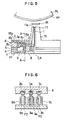
- Fig. 5 is a side view, half in section, showing the mechanical structure of a general spring-charge type wire-dot print head.
- a plate spring unit 3 comprises an annular support part 3b and radial parts 3a extending from the annular part 3b radially inward, i.e., toward the central axis CA of the disk-shaped rear yoke 7.
- Each of the radial parts 3a is also called a "plate spring”.
- Fixed to the free end of each plate spring radial part 3a is an armature 2.
- the annular part 3b of the plate spring 3 is rigidly clamped between the annular part 6b of the front yoke 6 and the intermediate yoke 5.
- the front yoke 6 also has a second annular part 6c continuous with the first annular part 6b and extending from the first annular part 6b to be positioned in front of the armatures 2, and radial parts 6a extending from the second annular part 6c rearwardly (downwardly as seen in Fig. 5) to be positioned between adjacent armatures 2.
- the armature 2 has a free end to which a rear end (base part) of a print wire 1 is rigidly attached.
- the tip (front end) of print wire 1 is arranged so that it can project through a guide aperture 11a of a wire guide 11 forming in the front end of the center of a front cover 15.
- the print wires 1 of the respective print elements are collected in the guide apertures 11a so that they are in a predetermined arrangement.
- the front cover 15 has an annular part 15b stacked on and fixed to the annular part 6b of the front yoke 6.
- cores 8 Located in the central portion of the rear yoke 7 are cores 8 on which coils 9 are wound, to form electromagnets.
- the cores 8 confront the rear surfaces of the armatures 1.
- Fig. 5 depicts only one of each for simplicity of illustration.
- the print wires 1, the armatures 2, the plate springs 3, the permanent magnet 4, the intermediate yoke 5, the front yoke 6, the rear yoke 7, the cores 8 and the coils 9 form print elements.
- the permanent magnet 4, the intermediate yoke 5, the front yoke 6, and the rear yoke 7 are common constituent parts, while the movable parts consisting of the print wires 1, the armatures 2 and the plate springs 3, and the electromagnets consisting of the cores 8 and the coils 9 are arranged in a ring on the rear yoke 7, to form a plurality of print elements.
- Fig. 6 is a section along line A-A of Fig. 5.
- reference marks 2a to 2c denote armatures
- reference marks 8a to 8c are cores
- reference marks 9a to 9c denote coils.
- the armatures 9a and the core 8a; the armature 9b and the core 8b; and the armature 9c and the core 8c respectively form electromagnets.
- Fig. 6 shows three electromagnets physically adjacent to each other in Fig. 5 and the corresponding armatures 2.
- each printing element in the print head is as follows:
- the magnetic flux from the permanent magnet 4 passes through a magnetic path consisting of the intermediate yoke 5, the front yoke 6, the armature 2, the core 8 and the rear yoke 7, along a loop indicated by arrow P1.
- the armature 2 is attracted to the core 8 because the distance between the armature 2 and the core 8 is shorter than the distance between the armature 2 and the rearwardly (downwardly, as seen in Fig. 5 and Fig.
- the coil 9 If, in this state, the coil 9 is energized, the magnetic flux developed in the core 8 by the coil 9 will cancel the magnetic flux developed by the permanent magnet 4. Therefore, the armature 2 will be released from the core 8. As a result, the plate spring 3a will restore its natural state, and the armature 2 and the print wire 1 are driven forward, and the tip of the print wire 1 will be ejected in the forward (upward as seen in the figure) direction through the guide aperture 11a in the front cover and will print a dot forming part of a character or other print output onto a printing paper PP through an ink ribbon IR placed between the tip of the wire 1 and the printing paper PP on a platen PL.
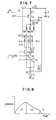
- Fig. 7 is a diagram of a drive circuit for the coils 9 in the prior-art wire-dot print head. Three electromagnets, shown in Fig. 6, are made to form a block for control of energization.
- first ends of the coils 9a to 9c are connected to the collector of a PNP transistor T-d for controlling the energization of the coils 9a to 9c.
- the emitter of the trasistor T-d is connected to a first, or positive terminal of a power supply E supplying electric energy to the coils 9a to 9c.
- Second ends of the coils 9a to 9c are connected to collectors of NPN transistors T-a, T-b and T-c which control the energization of the coils 9a to 9c individually and the anodes of diodes D-a, D-b and D-c.
- the cathodes of the diodes D-a, D-b and D-c are connected to the first terminal of the power supply E.
- the emitters of the transistors T-a, T-b and T-c are connected to the first ends of the coils 9a to 9c through a diode D-d for conducting a circulating current.
- the emitters of the transistors T-a, T-b and T-c are also connected to the ground 6.
- the second, or negative terminal of the power supply is also grounded.
- circuit configuration in other blocks is similar.
- the printing of one dot, in one printing cycle can be divided into three stages.
- the first stage lasts from the commencement of excitation of the selected electromagnet and until about the commencement of forward movement of the associated armature and the print wire.
- the second stage lasts from about the commencement of the forward movement of the armature and the print wire and until about the impact of the print wire on the printing paper.
- the third stage lasts from about the impact of the print wire on the printing paper and until the current due to an electromotive force induced in the coil ceases.
- the commencement of the forward movement of the armature and the print wire, and the impact of the print wire on the printing paper can be detected by means not shown, or assumed to occur at predetermined timings, by use of timing elements.
- Fig. 8 is a diagram showing the waveforms of the currents flowing through the coil 9a in the first, second and third stages.
- the parts [1], [2] and [3] correspond to the first, second and third stages, respectively.
- a signal DT1 applied to the transistor T-d is High, so the transistor T-d is ON, and also a signal DT-2 applied to the transistor T-a is High so the transistor T-a is ON.
- the other transistors T-b and T-c are kept OFF.
- the current flows, as shown by arrow [1], i.e., from the first terminal of the power supply E, then through the transistor T-d, then the coil 9a, and then the transistor T-a, and then to the ground. Because of this current, the electromagnet is excited to generate a magnetic flux and the associated armature and the print wire begin to move.
- the signal DT1 is Low, while the signal DT2 is High, so the transistor T-a is kept ON, while the transistor T-d is OFF.
- the coil 9a is isolated from the power supply E, an electromotive force induced in the coil 9a causes a current to flow through the path shown by arrow [2], i.e., from the coil 9a, then through the transistor T-a, and then the diode D-d, and then back to the coil 9a.
- the signal DT2 applied to the transistor T-a also Low, so the transistor T-a is also OFF. Because of the electromotive force still induced in the coil 9a, a current flows through the path as shown by arrow [3], from the ground, then through the diode D-a, then the coil 9a, and then the diode D-a, and then to the first terminal of the power supply E. This current rapidly diminishes.
- a problem associated with the prior art described above is that, induced by the electromagnet having a coil being energized, a current also flows through a coil of an electromagnet which is physically adjacent to the electromagnet having the coil being energized.
- the canceling magnetic flux that is created when the coil 9a of the electromagnet is energized not only flows through the core 8a in a direction opposite to the attracting magnetic flux of the permanent magnet 4, but also flows through the adjacent armatures 2b and 2c and cores 8b and 8c, along loops P2 and P3, to cause a magnetic interference
- the present invention has been made to solve these problems, and its object is to provide a wire-dot print head with a low power consumption in which unwanted induction current through an electromagnet which is physically adjacent to the coil of the electromagnet that is energized is eliminated or reduced.
- the invention provides a wire-dot print head in which the electromagnets are divided into a plurality of blocks each having two or more electromagnets, a common current conduction control element is provided for each block and used to control the current through the coils of the electromagnets in the block, wherein the electromagnets having the coils energized by a current which is passed through said common current conduction control element of each of at least some of all the blocks are disposed so as not to be physically adjacent to each other.
- the invention is featured by the unique wiring of the coils of the electromagnets and the current conduction control elements.
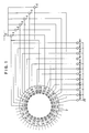
- Fig. 1 is a wiring diagram showing a first embodiment of the invention. More specifically, it is a diagram showing how the coils of the electromagnets and a transistor which is the common current conduction control element are connected.
- the positions of the coils 9-1 to 9-24 on the circle schematically representing the rear yoke 7 represent the physical positions of the electromagnets having the coils.
- reference marks 9-1 to 9-24 denote coils of the electromagnets corresponding to the those 9a to 9c in Fig. 7, and 12 odd-numbered coils 9-1 to 9-23 and 12 even-numbered coils 9-2 to 9-24 are disposed, being divided on the right side and left side of the rear yoke 7.
- the coils 9-1 to 9-24 are wound on the cores 8 (see Fig. 5), but the cores are not illustrated in Fig. 1.
- Reference marks T-1 to T-6 denote transistors which are common current conduction control elements corresponding to that T-d in Fig. 7.
- Reference marks T9-1 to T9-23 are transistors which are individual current conduction control elements corresponding to those T-a to T-c in Fig. 7.
- first ends of the coils 9-1 and 9-13 are connected together and connected through the transistor T1 to a first, positive terminal of a power supply E.
- first ends of the coils 9-3 and 9-15; first ends of the coils 9-5 and 9-17; first ends of the coils 9-7 and coils 9-19; first ends of the coils 9-9 and coils 9-21; and first ends of the coils 9-11 and 9-23 are connected together and through transistors T2 to T6 to the positive terminal of the power supply E.
- Second ends of the coils 9-1 to 9-23 are connected to the collectors of the transistors T9-1 to T9-23, respectively.
- two electromagnets are made to form a block, and the electromagnets belonging to the same block, i.e., having coils whose energization is controlled by a common current conduction control element, e.g., coils 9-1 and 9-13, are disposed so as not to be physically adjacent to each other on the rear yoke 7.
- a common current conduction control element e.g., coils 9-1 and 9-13
- the 12 even-numbered coils 9-2 to 9-24 are provided with transistors in a manner similar to that described with reference to the odd-numbered coils 9-1 to 9-23.
- the print elements in the print head are comprised of the print wire 1, the armatures 2, the plate spring 3, the permanent magnet 4, the intermediate yoke 5, the front yoke 6, the rear yoke 7, the cores 8 and the coils 9, as explained with reference to Fig. 5.
- the coils 9-3 and 9-15 of the electromagnets energized through a common current conduction control element are disposed so as not be physically adjacent to each other, as described above, so that when for example the coil 9-3 is energized and a magnetic flux passes through the cores of the adjacent electromagnets having coils 9-1 and 9-5, the current through the coils 9-1 and 9-5 of the adjacent electromagnets and the common current conduction control elements T-1 and T-3 for the adjacent electromagnets do not flow because the common current conduction control elements are OFF.
- the electromagnet whose coil 9-15 is connected to the same common current conduction control element T-2 is physically separated from the electromagnet having the coil 9-3, the magnetic flux from the electromagnet having the coil 9-3 is negligible so the current due to the magnetic interference is negligible.
- the wire-dot print head according to the present embodiment has the configuration shown in Fig. 1, while the prior-art wire-dot print head has the configuration shown in Fig. 4.
- the coils 9-1 and 9-3 of the electromagnets which are physically adjacent to each other are connected to a transistor T1.
- the coils 9-5 and 9-7 are connected to a transistor T2;
- the coils 9-9 and 9-11 are connected to a transistor T3;
- the coils 9-13 and 9-15 are connected to a transistor T4;
- the coils 9-17 and 9-19 are connected to a transistor T5; and
- the coils 9-21 and 9-23 are connected to a transistor T6.
- the two wire-dot print heads were used to print 100 characters arbitrarily selected.
- the average power consumption was as follows: Prior-art wire-dot print head: 212 watts
- Wire-dot print head of the present embodiment 201 watts
- wire-dot print head of the present embodiment is superior by about 5% to the prior-art wire-dot print head.
- the wire-dot print head of the present embodiment has a substantial advantage when the print pattern requires that several print wires adjacent to each other are driven simultaneously.
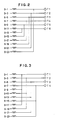
- Fig. 2 is a wiring diagram showing a second embodiment of the wire-dot print head according to the present invention.
- the coils are shown to be arranged along a line, but it should be understood that they are actually arranged along a circumference of a rear yoke.
- the coils 9-1 and 9-23 are connected to a transistor T1; the coils 9-3 and 9-21 are connected to a transistor T2; the coils 9-5 and 9-19 are connected to a transistor T3; the coils 9-7 and 9-17 are connected to a transistor T4; the coils 9-9 and 9-15 are connected to a transistor T5; the coils 9-11 and 9-13 are connected to a transistor T6.
- the coils 9-11 and 9-13 of the electromagnets positioned physically adjacent to each other are commonly controlled by the transistor T6.
- the coils 9-1 to 9-9 and 9-15 to 9-23 controlled by the transistors T1 to T-5 are not physically adjacent to each other. Accordingly, a result similar to that of the first embodiment is obtained.
- Fig. 3 is a wiring diagram showing a third embodiment of the wire-dot print head according to the invention.
- the coils are also shown to be arranged along a line, but it should be understood that they are actually arranged along a circumference of a rear yoke.
- the coils 9-1, 9-9, and 9-17 are connected to a transistor T1
- the coils 9-3, 9-11 and 9-19 are connected to a transistor T2
- the coils 9-5, 9-13 and 9-21 are connected to a transistor T3
- the coils 9-7, 9-15 and 9-23 are connected to a transistor T4.
- each block has three electromagnets, and each block is associated with transistors T1 to T4, and the electromagnets in each block are disposed so as not to be physically adjacent to each other.
- the present invention is not limited to the above-described embodiments, but various modifications can be made with respect to the wiring in view of the total number of electromagnets, and the number of the transistors which are the current conduction control elements.
- At least some of all the electromagnets having coils energized through a common current conduction control elements are disposed so as not to be physically adjacent to each other. As a result, the power consumption due to the magnetic interference between adjacent electromagnets is reduced.
- a wire-dot print head with a reduced power consumption can thereby be provided.
Landscapes
- Impact Printers (AREA)
Applications Claiming Priority (2)
| Application Number | Priority Date | Filing Date | Title |
|---|---|---|---|
| JP81241/88 | 1988-04-04 | ||
| JP63081241A JPH01253456A (ja) | 1988-04-04 | 1988-04-04 | ワイヤ印字ヘッド |
Publications (2)
| Publication Number | Publication Date |
|---|---|
| EP0339794A1 true EP0339794A1 (fr) | 1989-11-02 |
| EP0339794B1 EP0339794B1 (fr) | 1992-07-29 |
Family
ID=13740926
Family Applications (1)
| Application Number | Title | Priority Date | Filing Date |
|---|---|---|---|
| EP89303034A Expired - Lifetime EP0339794B1 (fr) | 1988-04-04 | 1989-03-28 | Tête d'impression par points à aiguilles |
Country Status (4)
| Country | Link |
|---|---|
| US (1) | US5071269A (fr) |
| EP (1) | EP0339794B1 (fr) |
| JP (1) | JPH01253456A (fr) |
| DE (1) | DE68902265T2 (fr) |
Cited By (1)
| Publication number | Priority date | Publication date | Assignee | Title |
|---|---|---|---|---|
| GB2235161B (en) * | 1989-08-09 | 1993-12-15 | Brother Ind Ltd | Driving circuit for solenoid head of a printer |
Citations (2)
| Publication number | Priority date | Publication date | Assignee | Title |
|---|---|---|---|---|
| US4286517A (en) * | 1979-07-12 | 1981-09-01 | Hitachi Koki Company Limited | Printer magnetic interference prevention system |
| US4473311A (en) * | 1982-03-31 | 1984-09-25 | Brother Kogyo Kabushiki Kaisha | Print wire drive assembly for dot-matrix printers |
Family Cites Families (3)
| Publication number | Priority date | Publication date | Assignee | Title |
|---|---|---|---|---|
| JPS58224762A (ja) * | 1982-06-23 | 1983-12-27 | Fujitsu Ltd | ワイヤドツト印字ヘツド |
| JPS60225768A (ja) * | 1984-04-25 | 1985-11-11 | Nec Corp | ドツト式シリアルプリンタのプリントヘツド駆動回路 |
| JPH0661941B2 (ja) * | 1985-11-13 | 1994-08-17 | 沖電気工業株式会社 | 印字ヘツド駆動方法 |
-
1988
- 1988-04-04 JP JP63081241A patent/JPH01253456A/ja active Pending
-
1989
- 1989-03-28 DE DE8989303034T patent/DE68902265T2/de not_active Expired - Fee Related
- 1989-03-28 EP EP89303034A patent/EP0339794B1/fr not_active Expired - Lifetime
- 1989-03-29 US US07/330,403 patent/US5071269A/en not_active Expired - Fee Related
Patent Citations (2)
| Publication number | Priority date | Publication date | Assignee | Title |
|---|---|---|---|---|
| US4286517A (en) * | 1979-07-12 | 1981-09-01 | Hitachi Koki Company Limited | Printer magnetic interference prevention system |
| US4473311A (en) * | 1982-03-31 | 1984-09-25 | Brother Kogyo Kabushiki Kaisha | Print wire drive assembly for dot-matrix printers |
Non-Patent Citations (2)
| Title |
|---|
| PATENT ABSTRACTS OF JAPAN vol. 11, no. 330 (M-636)(2777) 28 October 1987, & JP-A-62 113567 (SHUNICHI ITO ET AL) 25 May 1987, * |
| PATENT ABSTRACTS OF JAPAN, vol. 11, no. 330 (M-636)[2777], 28th October 1987; & JP-A-62 113 567 (OKI ELECTRIC IND. CO. LTD) 25-05-1987 * |
Cited By (1)
| Publication number | Priority date | Publication date | Assignee | Title |
|---|---|---|---|---|
| GB2235161B (en) * | 1989-08-09 | 1993-12-15 | Brother Ind Ltd | Driving circuit for solenoid head of a printer |
Also Published As
| Publication number | Publication date |
|---|---|
| EP0339794B1 (fr) | 1992-07-29 |
| DE68902265D1 (de) | 1992-09-03 |
| DE68902265T2 (de) | 1993-03-11 |
| JPH01253456A (ja) | 1989-10-09 |
| US5071269A (en) | 1991-12-10 |
Similar Documents
| Publication | Publication Date | Title |
|---|---|---|
| JPS63176157A (ja) | ドツト・マトリツクス・プリンタ用印刷ヘッド | |
| EP0339794B1 (fr) | Tête d'impression par points à aiguilles | |
| US4913569A (en) | Wire-type printing head | |
| US5241904A (en) | Dot like printer employing overlapped current applying sequence to coils of different groups | |
| US4472072A (en) | Printing apparatus | |
| EP0117145B1 (fr) | Tête d'impression à impact par points | |
| US5356228A (en) | Apparatus for driving adjacent elements in a wire-dot print head | |
| US5137380A (en) | Wire-dot print head | |
| JPH0661941B2 (ja) | 印字ヘツド駆動方法 | |
| JPS5836469A (ja) | ドット印字ヘッド | |
| JP3084338B2 (ja) | 印字ヘッドの印字制御方法 | |
| US5263782A (en) | Print hammer arrangement in dot line printer minimizing number of hammers simultaneously fired | |
| EP0365267B1 (fr) | Tête d'impression pour imprimante par points à impact | |
| EP0269959B1 (fr) | Tête d'impression de type à fils | |
| EP0366497A2 (fr) | Entraînement pour tête d'impression par points à aiguilles | |
| JP2881156B2 (ja) | ワイヤドット印字ヘッド | |
| JPS5919173A (ja) | ドツトラインプリンタにおける印字ヘツド | |
| JPS58168580A (ja) | 印字ヘツド | |
| JP3052526B2 (ja) | ドットインパクトハンマの駆動方式 | |
| JPH1044477A (ja) | ドットプリンタ | |
| JP2608182B2 (ja) | ワイヤドット印字ヘッド | |
| JP3678285B2 (ja) | ハンマ機構部 | |
| JP3857378B2 (ja) | インパクトプリンタ | |
| JP4300721B2 (ja) | 印刷装置の印刷密度制限方法 | |
| JPH06115115A (ja) | プリンタ |
Legal Events
| Date | Code | Title | Description |
|---|---|---|---|
| PUAI | Public reference made under article 153(3) epc to a published international application that has entered the european phase |
Free format text: ORIGINAL CODE: 0009012 |
|
| AK | Designated contracting states |
Kind code of ref document: A1 Designated state(s): DE FR GB |
|
| 17P | Request for examination filed |
Effective date: 19900118 |
|
| 17Q | First examination report despatched |
Effective date: 19910424 |
|
| GRAA | (expected) grant |
Free format text: ORIGINAL CODE: 0009210 |
|
| AK | Designated contracting states |
Kind code of ref document: B1 Designated state(s): DE FR GB |
|
| ET | Fr: translation filed | ||
| REF | Corresponds to: |
Ref document number: 68902265 Country of ref document: DE Date of ref document: 19920903 |
|
| PLBE | No opposition filed within time limit |
Free format text: ORIGINAL CODE: 0009261 |
|
| STAA | Information on the status of an ep patent application or granted ep patent |
Free format text: STATUS: NO OPPOSITION FILED WITHIN TIME LIMIT |
|
| 26N | No opposition filed | ||
| PGFP | Annual fee paid to national office [announced via postgrant information from national office to epo] |
Ref country code: FR Payment date: 19980310 Year of fee payment: 10 |
|
| PGFP | Annual fee paid to national office [announced via postgrant information from national office to epo] |
Ref country code: GB Payment date: 19980319 Year of fee payment: 10 |
|
| PGFP | Annual fee paid to national office [announced via postgrant information from national office to epo] |
Ref country code: DE Payment date: 19980403 Year of fee payment: 10 |
|
| PG25 | Lapsed in a contracting state [announced via postgrant information from national office to epo] |
Ref country code: GB Free format text: LAPSE BECAUSE OF NON-PAYMENT OF DUE FEES Effective date: 19990328 |
|
| GBPC | Gb: european patent ceased through non-payment of renewal fee |
Effective date: 19990328 |
|
| PG25 | Lapsed in a contracting state [announced via postgrant information from national office to epo] |
Ref country code: FR Free format text: LAPSE BECAUSE OF NON-PAYMENT OF DUE FEES Effective date: 19991130 |
|
| REG | Reference to a national code |
Ref country code: FR Ref legal event code: ST |
|
| PG25 | Lapsed in a contracting state [announced via postgrant information from national office to epo] |
Ref country code: DE Free format text: LAPSE BECAUSE OF NON-PAYMENT OF DUE FEES Effective date: 20000101 |