EP0339963A2 - Rectificateur synchrone - Google Patents
Rectificateur synchrone Download PDFInfo
- Publication number
- EP0339963A2 EP0339963A2 EP89304149A EP89304149A EP0339963A2 EP 0339963 A2 EP0339963 A2 EP 0339963A2 EP 89304149 A EP89304149 A EP 89304149A EP 89304149 A EP89304149 A EP 89304149A EP 0339963 A2 EP0339963 A2 EP 0339963A2
- Authority
- EP
- European Patent Office
- Prior art keywords
- voltage
- synchronous rectifier
- switching devices
- diode
- field effect
- Prior art date
- Legal status (The legal status is an assumption and is not a legal conclusion. Google has not performed a legal analysis and makes no representation as to the accuracy of the status listed.)
- Granted
Links
- 230000001360 synchronised effect Effects 0.000 title claims abstract description 58
- 239000004065 semiconductor Substances 0.000 claims abstract description 24
- 230000005669 field effect Effects 0.000 claims abstract description 17
- 239000000463 material Substances 0.000 claims abstract description 10
- 238000004804 winding Methods 0.000 claims description 22
- 230000002441 reversible effect Effects 0.000 claims description 8
- 238000011084 recovery Methods 0.000 claims description 5
- 230000001052 transient effect Effects 0.000 claims description 3
- 230000003071 parasitic effect Effects 0.000 abstract description 35
- 238000002955 isolation Methods 0.000 description 25
- 238000009825 accumulation Methods 0.000 description 10
- XUIMIQQOPSSXEZ-UHFFFAOYSA-N Silicon Chemical compound [Si] XUIMIQQOPSSXEZ-UHFFFAOYSA-N 0.000 description 9
- 210000000746 body region Anatomy 0.000 description 9
- 229910052710 silicon Inorganic materials 0.000 description 9
- 239000010703 silicon Substances 0.000 description 9
- 238000000034 method Methods 0.000 description 7
- 230000015556 catabolic process Effects 0.000 description 5
- 230000000694 effects Effects 0.000 description 5
- 239000000758 substrate Substances 0.000 description 5
- 230000008901 benefit Effects 0.000 description 4
- 230000007423 decrease Effects 0.000 description 4
- 238000009792 diffusion process Methods 0.000 description 4
- 238000004519 manufacturing process Methods 0.000 description 4
- 238000001020 plasma etching Methods 0.000 description 4
- 230000004044 response Effects 0.000 description 4
- 239000003990 capacitor Substances 0.000 description 3
- 238000006243 chemical reaction Methods 0.000 description 3
- 239000004020 conductor Substances 0.000 description 3
- 230000001627 detrimental effect Effects 0.000 description 3
- 230000015572 biosynthetic process Effects 0.000 description 2
- 230000006378 damage Effects 0.000 description 2
- 230000001419 dependent effect Effects 0.000 description 2
- 238000010586 diagram Methods 0.000 description 2
- 239000002019 doping agent Substances 0.000 description 2
- 239000007772 electrode material Substances 0.000 description 2
- 239000012212 insulator Substances 0.000 description 2
- 230000000670 limiting effect Effects 0.000 description 2
- 230000007246 mechanism Effects 0.000 description 2
- 230000004048 modification Effects 0.000 description 2
- 238000012986 modification Methods 0.000 description 2
- 230000008569 process Effects 0.000 description 2
- 230000002829 reductive effect Effects 0.000 description 2
- 230000003746 surface roughness Effects 0.000 description 2
- 230000002411 adverse Effects 0.000 description 1
- 238000010420 art technique Methods 0.000 description 1
- QVGXLLKOCUKJST-UHFFFAOYSA-N atomic oxygen Chemical compound [O] QVGXLLKOCUKJST-UHFFFAOYSA-N 0.000 description 1
- 230000004888 barrier function Effects 0.000 description 1
- 230000009286 beneficial effect Effects 0.000 description 1
- 230000000903 blocking effect Effects 0.000 description 1
- 239000000969 carrier Substances 0.000 description 1
- 230000008859 change Effects 0.000 description 1
- 239000002800 charge carrier Substances 0.000 description 1
- 238000001816 cooling Methods 0.000 description 1
- 239000011162 core material Substances 0.000 description 1
- 230000003247 decreasing effect Effects 0.000 description 1
- 230000001934 delay Effects 0.000 description 1
- 230000001747 exhibiting effect Effects 0.000 description 1
- 230000010354 integration Effects 0.000 description 1
- 239000002184 metal Substances 0.000 description 1
- 230000008520 organization Effects 0.000 description 1
- 238000013021 overheating Methods 0.000 description 1
- 229910052760 oxygen Inorganic materials 0.000 description 1
- 239000001301 oxygen Substances 0.000 description 1
- 229910021420 polycrystalline silicon Inorganic materials 0.000 description 1
- 229920005591 polysilicon Polymers 0.000 description 1
- 230000006798 recombination Effects 0.000 description 1
- 238000005215 recombination Methods 0.000 description 1
- 230000009467 reduction Effects 0.000 description 1
- 239000007787 solid Substances 0.000 description 1
Images


Classifications
-
- H—ELECTRICITY
- H10—SEMICONDUCTOR DEVICES; ELECTRIC SOLID-STATE DEVICES NOT OTHERWISE PROVIDED FOR
- H10D—INORGANIC ELECTRIC SEMICONDUCTOR DEVICES
- H10D30/00—Field-effect transistors [FET]
- H10D30/202—FETs having static field-induced regions, e.g. static-induction transistors [SIT] or permeable base transistors [PBT]
-
- H—ELECTRICITY
- H02—GENERATION; CONVERSION OR DISTRIBUTION OF ELECTRIC POWER
- H02M—APPARATUS FOR CONVERSION BETWEEN AC AND AC, BETWEEN AC AND DC, OR BETWEEN DC AND DC, AND FOR USE WITH MAINS OR SIMILAR POWER SUPPLY SYSTEMS; CONVERSION OF DC OR AC INPUT POWER INTO SURGE OUTPUT POWER; CONTROL OR REGULATION THEREOF
- H02M7/00—Conversion of AC power input into DC power output; Conversion of DC power input into AC power output
- H02M7/02—Conversion of AC power input into DC power output without possibility of reversal
- H02M7/04—Conversion of AC power input into DC power output without possibility of reversal by static converters
- H02M7/12—Conversion of AC power input into DC power output without possibility of reversal by static converters using discharge tubes with control electrode or semiconductor devices with control electrode
- H02M7/21—Conversion of AC power input into DC power output without possibility of reversal by static converters using discharge tubes with control electrode or semiconductor devices with control electrode using devices of a triode or transistor type requiring continuous application of a control signal
- H02M7/217—Conversion of AC power input into DC power output without possibility of reversal by static converters using discharge tubes with control electrode or semiconductor devices with control electrode using devices of a triode or transistor type requiring continuous application of a control signal using semiconductor devices only
-
- H—ELECTRICITY
- H10—SEMICONDUCTOR DEVICES; ELECTRIC SOLID-STATE DEVICES NOT OTHERWISE PROVIDED FOR
- H10D—INORGANIC ELECTRIC SEMICONDUCTOR DEVICES
- H10D30/00—Field-effect transistors [FET]
- H10D30/60—Insulated-gate field-effect transistors [IGFET]
- H10D30/63—Vertical IGFETs
- H10D30/635—Vertical IGFETs having no inversion channels, e.g. vertical accumulation channel FETs [ACCUFET] or normally-on vertical IGFETs
Definitions
- the present invention relates to the field of rectifier circuits and more particularly, to synchronous rectifier circuits.
- Rectifier means a device whose internal structure conducts current in one polarity, but blocks current flow in the opposing polarity. Rectifiers include diodes and SCRs. Such DC power supplies may employ either half-wave rectification in which a single rectifier is used or full-wave rectification in which a transformer, a bridge circuit and two discrete rectifiers are used in order to rectify both halves of an AC input voltage.
- Such DC power supplies in which the power supply DC output voltage is large compared to the ON-state voltage drop of the rectifier, provide fairly efficient conversion of an AC input voltage to a DC output voltage. However, as the power supply DC output voltage becomes a smaller multiple of the rectifier forward voltage drop, the power conversion efficiency of the power supply decreases because of an increase in the percentage of the AC input power which is dissipated in the rectifiers.
- One way of minimizing the power loss in the rectifying devices of a DC power supply is to use synchronous rectification rather than discrete rectifiers to convert the AC input voltage to a DC output voltage.
- the rectification is performed by semiconductor switching devices operating under the control of a synchronized timing circuit.
- the switching devices in a synchronous rectifier circuit are capable of conducting current in both directions and may be normally off until turned on by a control signal, or normally on until turned off by a control signal or may require a control signal for both turn on and turn off.
- rectifying device refers to a device which rectifies the AC current/voltage therethrough, independent of how it achieves that function.
- the term “rectifying device” includes the switching devices in a synchronous rectifier circuit as well as rectifiers per se.
- a control signal is provided to the switching device which causes it to be conductive when the voltage applied across it is of one polarity and to be non-conductive when the voltage applied across it is zero or of the opposite polarity.
- the rectifying device is a field effect transistor (FET) or another device whose forward voltage drop is less than that of a rectifier (diode)
- FET field effect transistor
- the portion of the applied power dissipated in the rectifying device of a synchronous rectifier circuit is reduced as compared to that dissipated in the rectifier for the same DC output voltage.
- Bipolar transistors, as well as FETs have been used as the rectifying devices in synchronous rectifier circuits.
- the rectifying devices used therein should have as small an inherent ON-state voltage drop as possible and should have as low an ON-resistance per unit area as possible.
- Prior art devices which have been used as rectifying devices in synchronous rectification either have an internal structure which limits the maximum frequency at which they can rectify high amplitude currents/voltages and/or include parasitic devices which prevent the synchronous rectifier from operating in an ideal manner.
- the maximum operating frequency of a FET synchronous rectifier circuit is limited by parasitic diodes and a parasitic bipolar transistor which are inherent in the FET.
- parasitic diodes within the FET becomes conductive at some stages in the operating cycle of a synchronous rectifier and cause switching noise which is present in the DC output voltage and may also interfere with the synchronous control system.
- the parasitic bipolar transistor in an FET can cause destruction of the FET under some circuit conditions.
- An embodiment of the present invention provides a synchronous rectifier circuit which is substantially free of parasitic bipolar transistor and diode devices.
- Another embodiment provides a synchronous rectifier system in which lossy parasitic diodes are prevented from becoming conductive.
- a further embodiment provides a synchronous rectifier system having fast diodes in place of slow diodes.
- Yet another embodiment of the present invention comprises a synchronous rectifier circuit in which the rectifying devices are field effect devices whose conductivity is controlled by an insulated gate and which are free of parasitic devices.
- These rectifying devices incorporate only a single conductivity type of semiconductor material and thus are free of PN junctions and parasitic bipolar and diode devices.
- High speed, low storage diodes such as Schottky diodes are connected in parallel with these rectifying devices to conduct transient currents with a minimal adverse effect on circuit performance.
- prior art FETs having an NPN or PNP internal structure may be used as the rectifying devices when Schottky diodes are connected in parallel to prevent the parasitic diodes in the FETs from becoming conductive.
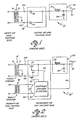
- FIG. 1 is a schematic diagram of the isolation transformer/rectifier stage 10 of a prior art full-wave rectifier power supply.
- This isolation transformer/rectifier stage comprises an isolation transformer 12, a DC output filter 20 and a rectification system 30.
- This portion of the power supply is also known as the rectifier stage.
- the transformer 12 has a primary winding 14 which is the input side of the transformer and which serves as the AC input for the isolation transformer/rectifier stage.
- Transformer 12 has a secondary winding 16 having a grounded center tap.
- a first diode rectifier 32 is connected between a first end 16a of the secondary winding and the output filter 20.
- a second diode rectifier 34 is connected between the second end 16b of the secondary winding and the output filter 20.
- Diodes 32 and 34 have their cathodes connected in common to the input of the output filter 20.
- the output filter 20 comprises an inductor 22 and a holding capacitor 24 which are connected in series between the common connection of the rectifiers and ground.
- the isolation/rectification stage output terminal 26 is connected to the common connection of the inductor 22 and the capacitor 24.
- each of the diodes dissipates power when it is conducting since it has an inherent, non-zero, ON-state voltage drop which is substantially independent of the current flow therethrough.
- the power dissipated in each diode is equal to the voltage drop across the diode when it is ON times the average current through the diode.
- this inherent ON-state voltage drop is about 0.7 volts, while for a silicon P-I-N diode it is about 0.9 volts and for a Schottky diode it is about 0.5 volts.
- the isolation transformer/rectification stage of a prior art synchronous rectifier circuit is shown in schematic form in Figure 2.
- the synchronous rectifier stage 10′ of Figure 2 is similar to the diode rectifier stage 10 of Figure 1 in having a transformer 12, an output filter 20, and a rectification section 40.
- the transformer 12 and the output filter 20 in the synchronous rectifier stage 10′ may be identical to those in the diode rectifier stage 10.
- the most significant structural differences between the synchronous rectifier stage 10′ and the diode rectifier stage 10 are in their rectification systems.
- the rectification system 40 of isolation/rectification stage 10′ replaces the diodes 32 and 34 of system 30 of isolation/rectification stage 10 with FETs 42 and 44, respectively.
- the connection of the FETs in the bridge circuit is similar to that of the diodes.
- FETs are active switches which in normal operation, are switched in response to control signals applied to them rather than in response to the voltage across them, an external control system 50 is required in order to produce rectification.
- the control system 50 has control lines 52 and 54 connected to the gate terminals of the field effect transistors 42 and 44, respectively, to control their conduction.
- control system 50 requires, as an input signal, either the AC signal applied to the primary winding 14 of the transformer 12 or a signal which provides the control system 50 with timing information as to the frequency of that AC signal and the timing of its zero crossings.
- this signal is provided through a small transformer 60 which has leads 62 connected to the control system 50.
- the turns ratio of the transformer 60 is determined in accordance with the input signal applied to ts primary side and the voltage range which is suitable for application to the control system 50.
- Control system 50 may also receive the output voltage E OUT of the isolation/rectification stage as an input signal on line 66.
- the design of the control system 50 may follow any of a number of well-known designs.
- the control system 50 applies a voltage to the control line 52 which renders the FET 42 conductive when the secondary terminal 16a is at a positive voltage. This enables current to flow from winding terminal 16a into the filter 20.
- an ON signal is applied to lead 52 during the period of time when the voltage at the secondary terminal 16a is positive.
- the signal on lead 52 is changed to an OFF signal to turn FET 42 OFF. What those control signals are is dependent on the particular type of FET employed.
- a conduction or ON signal is applied to the lead 54 to render the FET 44 conductive. That ON signal is maintained on the lead 54 until the voltage at terminal 16b of the secondary once again decreases to zero. Just before that voltage becomes zero, the signal on the lead 54 is changed back to a non-conduction or OFF signal to shut off FET 44.
- the ON-periods of the control signals on lines 52 and 54 for FETs 42 and 44, respectively are normally made slightly shorter than one half of the period of the input AC voltage in order to ensure that both FETs are not ON at the same time.
- the current through a diode and the voltage across it around the time of turn-off are shown in graphic form in Figure 8 for a reversal in the polarity of the voltage across it and the + and - convention for voltage shown adjacent to the diode symbol in Figure 8.
- the current is at a positive level while the diode is on and the voltage across the diode is equal to one forward voltage drop as shown to the left of the vertical axis.
- the voltage drops across these rectifying devices is significantly different.
- the voltage drop across the rectifying devices (FETs 42 and 44) in isolation/rectification stage 10′ is about the forward-biased-junction voltage of diodes 32 and 34 less than the voltage across the rectifying devices (diodes 32 and 34) in isolation/rectification stage 10.
- a structure which aids in reducing the FET ON-resistance is a trench or UMOSFET gate structure in which the channel runs vertically through the base region portion of the wafer and the gate electrode is located in trenches which extend into the semiconductor body from one surface.
- a similar structure is the vertical charge control FET (VCCFET) in which the channel of the device runs vertically through the thickness of a semiconductor wafer - this is the source of the word "vertical" in the device name. The conductivity of this FET is controlled by disposing the gate electrode in trenches extending into the wafer from one surface.
- Voltage applied to the gate electrode controls the conductivity of the semiconductor mesas which separate the gate electrode segments and for appropriate mesa structure enables the device to hold off a larger voltage than normal UMOSFETs. This is known as charge control and is the source of the words "charge control" in the device name.
- Further information on VCCFETs and thus fabrication is contained in JP-A-63/174373 corresponding to US Patent Application Serial No. 938,692 entitled “Semiconductor Devices Exhibiting Minimum On Resistance” and JP-A-63/155768 corresponding to US application Serial No. 938,666 entitled “Method of Fabricating a Semiconductor Device", and incorporated herein by reference in their entirety. The fabrication method described therein is easily adapted to produce devices as used in accordance with preferred embodiments of this invention.
- the AC input signal is often provided by an inverter operating from an input DC voltage which is different than the output voltage to be provided by the power supply. Consequently, the frequency of the AC signal which is applied to the transformer 12 can be selected by the designer in accordance with other requirements and is not dependent on the frequency of an externally available AC voltage. In order to minimize the size of the transformer 12 and, with appropriate core materials, its losses, high frequency operation is desirable.
- the frequency of operation increases, the time period availale for the parasitic diode to turn OFF is reduced.
- the maximum operating frequency of the synchronous rectifier is limited to between about 0.5 Mhz and about 2 Mhz by this diode turn-off time.
- FIG. 7 a prior art high voltage FET 110 is illustrated in cross section.
- the semiconductor portion of this FET comprises a drain region 112 which is heavily doped N type (N+), a drift region 114 which is lightly doped N type (N-), a body region 116 which is doped P type (P) and a source region 118 which is heavily doped N type (N+).
- the device illustrated is a vertical DMOSFET in which the drain region 112 forms the lower surface of the semiconductor wafer and the drift region, body region and source regions all extend to the upper surface of the wafer.
- a DMOSFET is a FET in which the length of the channel is determined by two successive diffusions (one P type and one N type) (known as double diffusion, thus the letter "D" in the device name) which are made through the same mask opening. The difference in lateral diffusion distance from the edge of the mask opening determines the channel length.
- a vertical DMOSFET is a DMOSFET in which the source and drain electrodes are on opposite surfaces of the semiconductor body which results in the main device current flowing vertically through the semiconductor wafer.
- a drain electrode 120 is disposed in ohmic contact with the drain region 112 along the lower surface of the wafer and has an external terminal marked D connected thereto.
- An insulated gate electrode 124 is spaced from the upper surface of the wafer by a gate insulating layer 122.
- the gate electrode 124 extends over the drift region where it extends to the upper surface, and over part of the source region and across the intervening portion of the body region 116. In this way, the potential of the gate electrode 124 relative to the body region 116 controls conduction through channels between the source regions 118 and the drift region 114.
- the gate electrode is indicated as having an external terminal G connected thereto.
- a source electrode 126 is disposed on the upper surface of the wafer, insulated from the gate electrode and in ohmic contact with the source region and the body region along the upper surface of the device and is illustrated as having an external terminal S connected thereto.
- the drain electrode D is held at a more positive voltage than the source electrode S.
- the PN junction 115 between the body region and the drift region is maintained in a reverse biased condition and the applied voltage tends to forward bias the PN junction 117 between the source region 118 and the body region 116.
- the source electrode 126 short circuits this diode and thereby under normal operating conditions prevents it from becoming forward biased. As a consequence, forward biasing of a diode does not occur during normal first quadrant operation of this device.
- This PN junction is not short circuited by any electrode, and is the parasitic diode which, in a synchronous rectification stage, turns ON to maintain current flow during the period that both FETs are OFF. Once turned ON, this diode injects holes into the drift region. This creates the stored charge in the "diode" which must be removed for the diode to turn OFF. Because of the high lifetime of carriers in the drift region, these stored holes take a long time to recombine and cause the long turn-off time for the diode, typically about 0.5 microseconds. This problem becomes significant as the operating frequency of the rectification stage is increased to more than about 0.5 Mhz or 1 MHz and limits the operating frequency to less than about 2 Mhz.
- the bipolar parasitic transistor of which the source region 118 and drift/drain region 114/112 are the emitter and collector, respectively, and of which the body region 116 is the base. Too rapid a change in the voltage (dv/dt) across the source and drain terminals of the device causes capacitance effects to provide a sufficient base current to turn ON that parasitic transistor before the FET can turn ON and short circuit that parasitic transistor.
- the effect of turning ON the parasitic bipolar transistor is similar to that of forward biasing the parasitic diode and can also result in a second breakdown of the FET, thereby limiting the safe operating area (SOA) of the device. This turn ON of the parasitic bipolar transistor can easily destroy the FET.
- the maximum dv/dt across the FET occurs near the zero-crossings of the AC voltage itself because that is the point in the AC voltage where dv/dt is a maximum.
- the maximum dv/dt increases with increasing frequency for a given AC voltage amplitude.
- the isolation/rectification stage of a synchronous rectifier circuit which overcomes the foregoing problems in accordance with the present invention is shown schematically in Figure 10.
- the output filter 20 has the input end of its inductor 22 connected to the common tap of the isolation transformer secondary winding.
- the first switching device 42′ is connected between a first outer end 16a of the secondary winding and ground.
- a Schottky diode 46 is connected in parallel with device 42′ with its anode connected to ground and its cathode connected to winding end 16a.
- a similar parallel connection between a second switching device 44′ and a second Schottky diode 48 is connected between a second outer end 16b of the secondary winding and ground.
- the two switching devices 42′ and 44′ there either are no internal parasitic diodes or else any parasitic diodes that may be present are prevented from turning on by the presence of the parallel Schottky diodes 46 and 48, respectively. Care must be exercised in selecting the Schottky diodes to be connected in parallel with a FET which includes a parasitic diode because the Schottky diode will only be effective to prevent the parasitic diode from turning ON if (1) the Schottky diode has a turn-on voltage which is less than the turn-on voltage of the parasitic diode and (2) the Schottky diode has an ON-state voltage drop which results in the voltage applied across the parasitic diode always being less than the parasitic diode's turn-on voltage.
- the diode which turns ON is either Schottky diode 46 or Schottky diode 48 depending on which portion of the secondary winding is conducting the current at that time. Since a Schottky diode has a recovery time which is in the range from a few nanoseconds up to about 50 nanoseconds, a number of benefits accrue. First, this synchronous rectifier circuit can be operated at much higher frequencies than synchronous rectifier circuits employing prior art field effect transistors as their switching devices because the turn-off time of the Schottky diodes does not limit circuit operating frequency unless that operating frequency is raised into the tens or hundreds of megahertz.
- the reverse current which flows in the secondary winding during the diode turn-off time is miniscule as compared to the current which flows when the parasitic diode in a prior art FET has to be turned OFF.
- switching devices 42′ and 44′ are shown as having separate Schottky diodes connected thereacross, these diodes are preferably integrated in the same chip with their associated respective devices 42′ and 44′, or even within the FET itself.
- Such integration provides the advantage of having a three terminal device (source, drain and gate) which can be directly substituted for a prior art FET in a synchronous rectifier and, more importantly for high frequency use, also minimizes inductances in the connection of the Schottky diodes. Any lead inductance between the Schottky diode and the FET results in delays at high frequencies with the result that the Schottky diode cannot act in an ideal manner. Thus, this minimization of inductance has a substantial beneficial effect on circuit operation.
- N-type field effect switching devices as the rectifying devices 42′ and 44′ in the isolation/rectification stage of a synchronous rectifier as shown in Figure 10 eliminates those parasitic devices which limit circuit operating frequencies.
- One such device 70 is illustrated in Figure 3.
- An orthogonal XYZ coordinate system is included in Figure 3 in order to provide an easy direction reference in the following description.
- the device 70 is an all N-type semiconductor device and contains no P-type semiconductor material.
- Device 70 comprises a body of semiconductor material 72 having a lower surface 74, an upper surface 76, and three layers 82, 84 and 86 of N type material having differing doping levels.
- the lowermost layer 82 is heavily doped N type (N+) and is referred to as the drain region of the device in accordance with normal FET terminology.
- Layer 82 should be doped to a donor dopant level of at least 1 x 10¹⁸ atoms/cm3. This layer may comprise the substrate portion of a semiconductor wafer on which the other layers are formed by epitaxial growth or other techniques.
- the layer 84 is disposed contiguous to the layer 82 and forms an interface 83 therewith.
- the layer 84 is referred to as the drift region of the device in accordance with common power FET terminology and is doped N type, but to a lesser conductivity level than the layer 82.
- the layer 84 in this embodiment may preferably have an N type doping level in the range from 5 x 10¹⁵ to 1 x 10¹⁷ atoms/cms, with a doping level of 4 x 10¹⁶ atoms/cm3 being preferred for a 50 volt device.
- the third layer 86 is disposed on top of and contiguous with the layer 84 in the drawings and forms an interface 85 therewith. Layer 86 is referred to as the source region and should be doped to at least 1 x 10¹⁸ donor dopant atoms/cm3.
- a trench structure 78 extends into the body 72 from the upper surface 76 in the drawing and defines or creates a mesa structure 79 which extends from the bottom of the trench to the upper surface 76 of the semiconductor body.
- the trenches have an X-direction trench width W T .
- the trench structure 78 extends through the source region 86 into the drift region 84 of the device.
- the trench 78 in this device does not extend entirely through the drift region 84 and thus is spaced from the drain region 82.
- the side wall surfaces of the mesa and the bottoms of the trenches 78 are oxidized or otherwise have a gate insulating layer formed thereon.
- the rest of the trench is filled with a gate electrode material 94, except for the very top of the trench just under the source electrode 96 where an insulating layer 95 is disposed to insulate the gate electrode from the source electrode.
- This is a normally ON device.
- the width W M of the mesas 79 in the X direction is made small enough that application of an appropriate bias voltage to the conductive portion of the insulated gate electrode 94 pinches off the drift layer segment of the mesa. This causes the device to be non-conductive between its source electrode 96 and its drain electrode 92.
- the width W M of the mesa in silicon may preferably be in the range of 1 to 5 microns. A value of about 1 microns is preferred.
- the non-conductive state is a first state of the device and is a result of the voltage on the gate electrode relative to the voltage in the drift region being sufficiently negative that depletion and pinch off of the drift region results.
- a second, conductive state of the device results from the gate electrode being at a less negative voltage which enables the drift region segment of the mesa to have many mobile charge carriers therein and hence to be highly conductive.
- a device of this type designed to withstand a voltage of 25 to 50 volts applied across its source and drain electrodes when it is being held in an OFF state without breaking down and becoming conductive should have a minimum specific ON-state resistance of about 0.1 milliohm-cm2 for source and drain doping levels of 1 x 10¹⁹ atoms/cm3, a drift region doping level of about 4 x 10¹⁶ atoms/cm3, an overall device thickness of 10 mils and a drift region thickness of 3 mils, with the width W M being 1 micron and the width W T of the trenches being 1 micron.
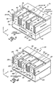
- a preferred all N-type FET 170 is shown in Figure 4 in a perspective cross-sectional view. Corresponding structures in the two devices 70 and 170 have been provided with corresponding reference numbers with the reference numerals in device 170 of Figure 4 increased by 100 relative to those of Figure 3.
- Device 170 is structurally and operationally very different from device 70 in that the doping level of the drift region 184 of device 170 is substantially lower than that of drift region 84 in device 70 of Figure 3 and for the same voltage rating the drift region 184 is substantially thinner than the drift region 84 of device 70.
- drift region 184 it is preferred to dope drift region 184 to between 1 x 10¹³ and 1 x 10¹⁷ donor atoms/cm3, with a doping level of 5 x 10¹³ atoms/cm3 being preferred for a 50 volt device.
- the trenches 178 in device 170 extend entirely through the drift region 184 into the drain region 182 so that the mesa 179 has its base in the drain region and the insulated gate electrode 194 extends the full vertical height of the drift region 184.
- the device 170 is rendered non-conductive through the depletion of the mesa segment of the drift region 184 in one state as a result of the relative voltage between the gate electrode 194 and the drift region 184 and in a second state is rendered conductive as a result of the relative potential between the gate electrode 194 and the drift region 184.
- it differs significantly from device 70 as a result of the low doping level of the drift region 184, which enables device 170 to be rendered non-conductive at a zero voltage differential between the drift region 184 and the gate electrode 194 by appropriate selection of the gate electrode material. This is a normally-OFF device.
- This potential difference can be applied between the source electrode and the gate electrode since the source and drift regions are in direct ohmic contact.
- This gate material may be a doped polysilicon, a metal or other appropriate conductive material. Alternatively, this device can be designed to be normally ON.
- the normally-OFF device is rendered conductive by applying a positive voltage to the gate electrode 194 relative to the drift region 184.
- This positive voltage causes an accumulation layer of electrons to form adjacent to the gate electrode along each of the vertical edges of the drift region 184 as shown by the dashed lines in Figure 4.
- this accumulation layer extends from the source region 186 to the drain region 182.
- This accumulation layer is highly conductive because it contains a high density of mobile electrons therein and because electrons have a high mobility in silicon. Further, because this gate-voltage-induced concentration of electrons is an accumulation layer, the electron mobility therein decreases only slightly as a result of surface roughness at the interface between the drift region 184 and the gate insulator 193.
- accumulation layer mobility is between three and four times larger than inversion layer mobility.
- the normally-ON device is made conductive at zero volts by a combination of selection of the drift region doping level and the gate electrode composition.
- the normally-ON device is rendered non-conductive by applying a negative voltage to the gate electrode 194 relative to the drift region.
- the resistance of this normally-ON device is not at its minimum value at a gate bias voltage of zero volts because of the low doping level in the drift region. Therefore, it is desirable to apply a positive gate bias voltage to obtain minimum ON-resistance.
- the gate electrodes In this accumulation mode device it is important, in order to obtain minimum ON-resistance, that the gate electrodes extend through the full thickness of the low-doping-level drift region so that the accumulation layer will extend from the source region to the drain region without any gap. A gap in the accumulation layer between the source and drain regions would reduce the overall conductivity of the device.
- An accumulation device in accordance with this embodiment having an overall thickness of 5 mils and a drift region thickness of 3 microns with a doping level of about 5 x 10¹³, with 3 micron wide trenches and 3 micron wide mesas, should have a specific ON-resistance of about 0.025 milliohm-cm2 under accumulation using a gate bias of 10 volts across a 500 Angstrom thick gate oxide. This is a factor of 8 better than the prior art 25 volt structure and is substantially better than is obtained with device 70 of Figure 3 or any prior art field effect transistor structure and is a substantial advantage in reducing the voltage drop across the switching devices of a synchronous rectifier.
- the device of Figure 4 is shown with the trenches and the gate electrodes arranged in parallel straight lines which extend in the Y-direction in the figures.
- This structure is presently preferred.
- the invention can alternatively be embodied in any desired trench configuration including, but not limited to, trenches which leave hexagonal, rectangular, circular or other shape mesas.
- FIG. 5 One example of an alternative mesa configuration is shown in Figure 5 where the device 170′ contains a plurality of spaced apart rectangular mesas 179′ in which the source region segment and the drift region segment of each mesa are spaced apart from all other source and drift region segments by the trenches 178′ and the gate electrode 194′ therein. This provides an interconnected gate electrode.
- the various mesa segments appear to be unconnected. However, they may be connected in a portion of the device which is not shown in this figure whereby there is only one, continuous mesa in the device.
- a structure is shown explicitly in Figure 6 where, in the device 170 ⁇ , the mesa structure 179 ⁇ includes a cross connecting portion and the trench structure 178 ⁇ comprises a plurality of separate trenches.
- care must be taken that the portion of the mesa at the crossing center (where the cross connection crosses one of the parallel Y direction segments) is close enough to the gate electrode segments 194 ⁇ that it becomes depleted when the depletion potential is applied to the gate electrode.
- each portion of the structure has the same reference numeral as it has in Figure 4. Those whose configuration is significantly changed have the same suffix (′ or ⁇ ) as the device number in that figure.
- the exceedingly low specific ON-resistance of the preferred devices makes the contact resistances between the source electrode and source region and the drain electrode and the drain region critical contributors to the overall ON-state voltage drop of the device. Consequently, to obtain the full benefit of the semiconductor structure of this device, very low resistance source and drain electrode contacts must be included in the device. To this end, silicided contacts are presently considered desirable.
- the device of Figure 4 can be designed to hold off maximum applied voltages of up to 50 volts. For higher voltages, device internal breakdown voltages become a significant concern because of the need for the gate dielectric to support the full source-to-drain voltage across the device in the OFF state. The breakdown voltage can be increased by using a thicker oxide layer near the bottom of the trenches. Special designs must be used if the maximum voltage is increased significantly in silicon devices.
- Devices with maximum voltage of 25 to 50 volts can meet all of the circuit requirements for properly designed synchronous rectification stages having DC output voltages ranging up to about 5 volts.
- devices may alternatively be designed as lateral devices if desired.
- lateral devices require care in their design in order to provide specific On-resistances as low as in the vertical versions of the device built with the same design rules.
- the devices are preferably fabricated by first forming the three layers (drain, drift and source) as a wafer having substantially planar surfaces. This may be done by epitaxial growth of the drift and source layers on a drain layer substrate or by diffusion of source and drain layers into a drift layer substrate.
- the substrate is the drain region
- the drift region is epitaxially grown on the drain region substrate and the source region is diffused into the drift region.
- the trenches are then formed by appropriate removal processes such as reactive ion etching (RIE). Thereafter the mesa side walls and trench bottoms are oxidized to form the gate insulator. A thicker oxide layer near the bottom of the trench and/or rounding the bottom of the trench is desirable where breakdown at the trench bottom is a concern.
- a thicker oxide may be provided on the bottom of the trenches by implanting oxygen into the silicon at the bottom of the trenches prior to growth of the gate oxide.
- the trenches are formed by RIE, it is desirable to grow and remove a layer of oxide prior to growing the gate oxide in order to remove some of the damage created by the RIE process.
- this is less necessary with this all N-type structure than it would be with an NPN structure.
- the gate conductor is deposited in the trenches and an insulating layer is formed over the gate conductor. Thereafter source and drain electrodes are formed on the source and drain regions, respectively. Other fabrication methods may alternatively be used. Further information on the formation of devices of this general structure may be found in the above-identified application JP-A-63/174373 and especially the method application JP-A-63/155768.
- While the devices of Figures 4-6 have each been shown as three layer devices having a source region, drift region and a drain region with each of these three regions having only one part, these devices may alternatively be fabricated with the drift region having two or more different segments, each having a different doping level in accordance with specific desired operating characteristics.
- the use of all N-type devices in accordance with this invention as the rectifying devices in a synchronous rectifier circuit increases its potential operating frequency to well in excess of 1 MHz and thereby eliminates the operating characteristics of the rectifying devices as the frequency limiting component of the synchronous rectifier circuit system.
Landscapes
- Engineering & Computer Science (AREA)
- Power Engineering (AREA)
- Rectifiers (AREA)
- Dc-Dc Converters (AREA)
- Electronic Switches (AREA)
Applications Claiming Priority (2)
| Application Number | Priority Date | Filing Date | Title |
|---|---|---|---|
| US07/186,983 US4903189A (en) | 1988-04-27 | 1988-04-27 | Low noise, high frequency synchronous rectifier |
| US186983 | 1988-04-27 |
Publications (3)
| Publication Number | Publication Date |
|---|---|
| EP0339963A2 true EP0339963A2 (fr) | 1989-11-02 |
| EP0339963A3 EP0339963A3 (en) | 1990-05-23 |
| EP0339963B1 EP0339963B1 (fr) | 1994-03-02 |
Family
ID=22687121
Family Applications (1)
| Application Number | Title | Priority Date | Filing Date |
|---|---|---|---|
| EP89304149A Expired - Lifetime EP0339963B1 (fr) | 1988-04-27 | 1989-04-26 | Rectificateur synchrone |
Country Status (4)
| Country | Link |
|---|---|
| US (1) | US4903189A (fr) |
| EP (1) | EP0339963B1 (fr) |
| JP (1) | JPH0213268A (fr) |
| DE (1) | DE68913334T2 (fr) |
Cited By (7)
| Publication number | Priority date | Publication date | Assignee | Title |
|---|---|---|---|---|
| EP0529180A1 (fr) * | 1991-08-30 | 1993-03-03 | Alcatel Bell-Sdt S.A. | Détecteur de courant alternatif et circuit d'alimentation en puissance |
| EP0616371A3 (fr) * | 1993-03-18 | 1995-08-02 | Canon Kk | Dispositif semiconducteur en Silicium sur isolant et méthode pour sa fabrication. |
| WO1998015011A1 (fr) * | 1996-09-30 | 1998-04-09 | Siemens Aktiengesellschaft | Transistor mos de puissance |
| EP0817361A3 (fr) * | 1996-06-24 | 1999-05-19 | Harris Corporation | Alimentation de puissance insensible à la charge |
| WO2001099266A1 (fr) * | 2000-06-23 | 2001-12-27 | Compact Dynamics Gmbh | Composants demi-pont |
| EP1659671A3 (fr) * | 1999-11-05 | 2006-05-31 | Nec Tokin Corporation | Accumulateur pourvu d'une commande d'énergie de cellules et procédé de commande de cette énergie |
| WO2020043766A1 (fr) * | 2018-08-29 | 2020-03-05 | Robert Bosch Gmbh | Transistor de puissance unipolaire en carbure de silicium |
Families Citing this family (94)
| Publication number | Priority date | Publication date | Assignee | Title |
|---|---|---|---|---|
| US4998151A (en) * | 1989-04-13 | 1991-03-05 | General Electric Company | Power field effect devices having small cell size and low contact resistance |
| US5111253A (en) * | 1989-05-09 | 1992-05-05 | General Electric Company | Multicellular FET having a Schottky diode merged therewith |
| US5183775A (en) * | 1990-01-23 | 1993-02-02 | Applied Materials, Inc. | Method for forming capacitor in trench of semiconductor wafer by implantation of trench surfaces with oxygen |
| JPH05211239A (ja) * | 1991-09-12 | 1993-08-20 | Texas Instr Inc <Ti> | 集積回路相互接続構造とそれを形成する方法 |
| US5179512A (en) * | 1991-09-18 | 1993-01-12 | General Electric Company | Gate drive for synchronous rectifiers in resonant converters |
| DE69312509T2 (de) | 1992-05-29 | 1998-02-26 | Minnesota Mining And Mfg. Co., Saint Paul, Minn. | Rückschlagventil |
| US5544038A (en) * | 1992-09-21 | 1996-08-06 | General Electric Company | Synchronous rectifier package for high-efficiency operation |
| US5303138A (en) * | 1993-04-29 | 1994-04-12 | At&T Bell Laboratories | Low loss synchronous rectifier for application to clamped-mode power converters |
| US5365102A (en) * | 1993-07-06 | 1994-11-15 | North Carolina State University | Schottky barrier rectifier with MOS trench |
| US5323040A (en) * | 1993-09-27 | 1994-06-21 | North Carolina State University At Raleigh | Silicon carbide field effect device |
| US5514604A (en) * | 1993-12-08 | 1996-05-07 | General Electric Company | Vertical channel silicon carbide metal-oxide-semiconductor field effect transistor with self-aligned gate for microwave and power applications, and method of making |
| US5396085A (en) * | 1993-12-28 | 1995-03-07 | North Carolina State University | Silicon carbide switching device with rectifying-gate |
| US5471075A (en) * | 1994-05-26 | 1995-11-28 | North Carolina State University | Dual-channel emitter switched thyristor with trench gate |
| US5488236A (en) * | 1994-05-26 | 1996-01-30 | North Carolina State University | Latch-up resistant bipolar transistor with trench IGFET and buried collector |
| EP0691729A3 (fr) * | 1994-06-30 | 1996-08-14 | Sgs Thomson Microelectronics | Circuit pompe de charge à commande asservi |
| US5581100A (en) * | 1994-08-30 | 1996-12-03 | International Rectifier Corporation | Trench depletion MOSFET |
| EP0729259B1 (fr) * | 1995-02-01 | 2003-06-04 | Advanced Micro Devices, Inc. | Génération d'un signal de sonnerie dans un circuit d'abonné (SLIC) |
| US5590032A (en) | 1995-05-25 | 1996-12-31 | Lucent Technologies Inc. | Self-synchronized drive circuit for a synchronous rectifier in a clamped-mode power converter |
| US5856692A (en) * | 1995-06-02 | 1999-01-05 | Siliconix Incorporated | Voltage-clamped power accumulation-mode MOSFET |
| US5661322A (en) * | 1995-06-02 | 1997-08-26 | Siliconix Incorporated | Bidirectional blocking accumulation-mode trench power MOSFET |
| US5679966A (en) * | 1995-10-05 | 1997-10-21 | North Carolina State University | Depleted base transistor with high forward voltage blocking capability |
| US5757038A (en) * | 1995-11-06 | 1998-05-26 | International Business Machines Corporation | Self-aligned dual gate MOSFET with an ultranarrow channel |
| US5637898A (en) * | 1995-12-22 | 1997-06-10 | North Carolina State University | Vertical field effect transistors having improved breakdown voltage capability and low on-state resistance |
| US5744994A (en) * | 1996-05-15 | 1998-04-28 | Siliconix Incorporated | Three-terminal power mosfet switch for use as synchronous rectifier or voltage clamp |
| US5825079A (en) * | 1997-01-23 | 1998-10-20 | Luminous Intent, Inc. | Semiconductor diodes having low forward conduction voltage drop and low reverse current leakage |
| US7269034B2 (en) | 1997-01-24 | 2007-09-11 | Synqor, Inc. | High efficiency power converter |
| JP2002514378A (ja) | 1997-01-24 | 2002-05-14 | シンクォール・インコーポレーテッド | 高効率電力変換装置 |
| US7272021B2 (en) * | 1997-01-24 | 2007-09-18 | Synqor, Inc. | Power converter with isolated and regulated stages |
| US5818704A (en) * | 1997-04-17 | 1998-10-06 | International Rectifier Corporation | Synchronizing/driving circuit for a forward synchronous rectifier |
| US5815384A (en) * | 1997-05-14 | 1998-09-29 | The United States Of American As Represented By The Secretary Of The Navy | Transformer which uses bi-directional synchronous rectification to transform the voltage of an input signal into an output signal having a different voltage and method for effectuating same |
| US5912497A (en) * | 1997-08-06 | 1999-06-15 | North Carolina State University | Semiconductor switching devices having buried gate electrodes and methods of forming same |
| US5907481A (en) * | 1997-10-31 | 1999-05-25 | Telefonaktiebolaget Lm Ericsson | Double ended isolated D.C.--D.C. converter |
| US6081432A (en) | 1998-05-26 | 2000-06-27 | Artesyn Technologies, Inc. | Active reset forward converter employing synchronous rectifiers |
| US6351018B1 (en) * | 1999-02-26 | 2002-02-26 | Fairchild Semiconductor Corporation | Monolithically integrated trench MOSFET and Schottky diode |
| US6694438B1 (en) * | 1999-07-02 | 2004-02-17 | Advanced Energy Industries, Inc. | System for controlling the delivery of power to DC computer components |
| US6331455B1 (en) * | 1999-04-01 | 2001-12-18 | Advanced Power Devices, Inc. | Power rectifier device and method of fabricating power rectifier devices |
| US6186408B1 (en) | 1999-05-28 | 2001-02-13 | Advanced Power Devices, Inc. | High cell density power rectifier |
| US6380569B1 (en) * | 1999-08-10 | 2002-04-30 | Rockwell Science Center, Llc | High power unipolar FET switch |
| US6420757B1 (en) | 1999-09-14 | 2002-07-16 | Vram Technologies, Llc | Semiconductor diodes having low forward conduction voltage drop, low reverse current leakage, and high avalanche energy capability |
| US6232752B1 (en) * | 1999-11-10 | 2001-05-15 | Stephen R. Bissell | DC/DC converter with synchronous switching regulation |
| US6285060B1 (en) * | 1999-12-30 | 2001-09-04 | Siliconix Incorporated | Barrier accumulation-mode MOSFET |
| US6433370B1 (en) | 2000-02-10 | 2002-08-13 | Vram Technologies, Llc | Method and apparatus for cylindrical semiconductor diodes |
| US6301139B1 (en) | 2000-04-06 | 2001-10-09 | Power-One, Inc. | Self-driven synchronous rectifier circuit for non-optimal reset secondary voltage |
| US6580150B1 (en) | 2000-11-13 | 2003-06-17 | Vram Technologies, Llc | Vertical junction field effect semiconductor diodes |
| US6537860B2 (en) | 2000-12-18 | 2003-03-25 | Apd Semiconductor, Inc. | Method of fabricating power VLSI diode devices |
| FI120310B (fi) * | 2001-02-13 | 2009-09-15 | Valtion Teknillinen | Parannettu menetelmä erittyvien proteiinien tuottamiseksi sienissä |
| US6385058B1 (en) * | 2001-05-17 | 2002-05-07 | Northrop Grumman | Active bleed voltage balancing circuit |
| US6537921B2 (en) | 2001-05-23 | 2003-03-25 | Vram Technologies, Llc | Vertical metal oxide silicon field effect semiconductor diodes |
| GB0120595D0 (en) * | 2001-08-24 | 2001-10-17 | Koninkl Philips Electronics Nv | A semiconductor rectifier |
| US6642738B2 (en) | 2001-10-23 | 2003-11-04 | Fairchild Semiconductor Corporation | Method and apparatus for field-effect transistor current sensing using the voltage drop across drain to source resistance that eliminates dependencies on temperature of the field-effect transistor and/or statistical distribution of the initial value of drain to source resistance |
| US7078296B2 (en) | 2002-01-16 | 2006-07-18 | Fairchild Semiconductor Corporation | Self-aligned trench MOSFETs and methods for making the same |
| US6958275B2 (en) * | 2003-03-11 | 2005-10-25 | Integrated Discrete Devices, Llc | MOSFET power transistors and methods |
| US6987305B2 (en) * | 2003-08-04 | 2006-01-17 | International Rectifier Corporation | Integrated FET and schottky device |
| US7368777B2 (en) * | 2003-12-30 | 2008-05-06 | Fairchild Semiconductor Corporation | Accumulation device with charge balance structure and method of forming the same |
| US20060073024A1 (en) * | 2004-09-17 | 2006-04-06 | Nanocoolers, Inc. | Series gated secondary loop power supply configuration for electromagnetic pump and integral combination thereof |
| US7339208B2 (en) * | 2005-05-13 | 2008-03-04 | Coldwatt, Inc. | Semiconductor device having multiple lateral channels and method of forming the same |
| US7675090B2 (en) * | 2005-05-13 | 2010-03-09 | Flextronics International Usa, Inc. | Semiconductor device having a contact on a buffer layer thereof and method of forming the same |
| DE102006009942B4 (de) * | 2006-03-03 | 2012-02-09 | Infineon Technologies Austria Ag | Laterales Halbleiterbauelement mit niedrigem Einschaltwiderstand |
| US8461648B2 (en) | 2005-07-27 | 2013-06-11 | Infineon Technologies Austria Ag | Semiconductor component with a drift region and a drift control region |
| US8110868B2 (en) * | 2005-07-27 | 2012-02-07 | Infineon Technologies Austria Ag | Power semiconductor component with a low on-state resistance |
| WO2007012490A2 (fr) | 2005-07-27 | 2007-02-01 | Infineon Technologies Austria Ag | Composant a semi-conducteurs comportant une zone de derive et une zone de commande de derive |
| US7285807B2 (en) * | 2005-08-25 | 2007-10-23 | Coldwatt, Inc. | Semiconductor device having substrate-driven field-effect transistor and Schottky diode and method of forming the same |
| DE102005043916B3 (de) * | 2005-09-14 | 2006-12-21 | Infineon Technologies Austria Ag | Leistungshalbleiterbauelement mit einer Feldelektrode und Verfahren zu dessen Herstellung |
| DE102005045910B4 (de) * | 2005-09-26 | 2010-11-11 | Infineon Technologies Austria Ag | Laterales SOI-Bauelement mit einem verringerten Einschaltwiderstand |
| DE102005047056B3 (de) * | 2005-09-30 | 2007-01-18 | Infineon Technologies Ag | Leistungshalbleiterbauelement mit einer Feldelektrodenstruktur und Verfahren zur Herstellung einer Feldelektrodenstruktur |
| US8368165B2 (en) | 2005-10-20 | 2013-02-05 | Siliconix Technology C. V. | Silicon carbide Schottky diode |
| JP2007142015A (ja) * | 2005-11-16 | 2007-06-07 | Hitachi Ltd | 半導体装置 |
| US7446374B2 (en) | 2006-03-24 | 2008-11-04 | Fairchild Semiconductor Corporation | High density trench FET with integrated Schottky diode and method of manufacture |
| US8415737B2 (en) * | 2006-06-21 | 2013-04-09 | Flextronics International Usa, Inc. | Semiconductor device with a pillar region and method of forming the same |
| US7663183B2 (en) * | 2006-06-21 | 2010-02-16 | Flextronics International Usa, Inc. | Vertical field-effect transistor and method of forming the same |
| US8154073B2 (en) | 2006-07-14 | 2012-04-10 | Denso Corporation | Semiconductor device |
| JP2008277324A (ja) * | 2007-04-25 | 2008-11-13 | Denso Corp | 縦型mosfetを有する半導体装置 |
| KR101193453B1 (ko) | 2006-07-31 | 2012-10-24 | 비쉐이-실리코닉스 | 실리콘 카바이드 쇼트키 다이오드를 위한 몰리브덴 장벽 금속 및 제조방법 |
| DE102006055742B4 (de) * | 2006-11-25 | 2011-07-14 | Infineon Technologies Austria Ag | Halbleiterbauelementanordnung mit mehreren zu einer Driftzone benachbart angeordneten Steuerelektroden |
| DE102007002965A1 (de) | 2007-01-19 | 2008-07-24 | Infineon Technologies Ag | Verfahren zur Herstellung einer kapazitiven Struktur oder Varistorstruktur in einem Graben eines Halbleiterkörper |
| DE102007004331B4 (de) | 2007-01-29 | 2014-08-21 | Infineon Technologies Austria Ag | Halbleiterbauelement mit reduziertem mechanischen Stress |
| DE102007004323A1 (de) * | 2007-01-29 | 2008-07-31 | Infineon Technologies Austria Ag | Bauelementanordnung mit einem eine Feldelektrode aufweisenden MOS-Transistor |
| US7888200B2 (en) * | 2007-01-31 | 2011-02-15 | Sandisk 3D Llc | Embedded memory in a CMOS circuit and methods of forming the same |
| US7868388B2 (en) * | 2007-01-31 | 2011-01-11 | Sandisk 3D Llc | Embedded memory in a CMOS circuit and methods of forming the same |
| US7564099B2 (en) * | 2007-03-12 | 2009-07-21 | International Rectifier Corporation | Monolithic MOSFET and Schottky diode device |
| DE102007042771C5 (de) * | 2007-09-07 | 2015-02-12 | Robert Bosch Gmbh | Verfahren zum Betrieb der Stromversorgung einer Widerstansschweißvorrichtung |
| EP2232559B1 (fr) | 2007-09-26 | 2019-05-15 | STMicroelectronics N.V. | Redresseur à effet de champ ajustable |
| US8148748B2 (en) * | 2007-09-26 | 2012-04-03 | Stmicroelectronics N.V. | Adjustable field effect rectifier |
| EP2384518B1 (fr) * | 2009-01-06 | 2019-09-04 | STMicroelectronics N.V. | Structures de diode à effet de champ à auto-amorçage et procédés correspondants |
| WO2010127370A2 (fr) * | 2009-05-01 | 2010-11-04 | Lakota Technologies, Inc. | Dispositif de limitation de courant série |
| US10205017B2 (en) * | 2009-06-17 | 2019-02-12 | Alpha And Omega Semiconductor Incorporated | Bottom source NMOS triggered Zener clamp for configuring an ultra-low voltage transient voltage suppressor (TVS) |
| US8969154B2 (en) | 2011-08-23 | 2015-03-03 | Micron Technology, Inc. | Methods for fabricating semiconductor device structures and arrays of vertical transistor devices |
| JP5472354B2 (ja) * | 2012-03-28 | 2014-04-16 | 株式会社村田製作所 | スイッチング電源装置 |
| DE102012025202A1 (de) | 2012-12-27 | 2014-07-03 | Robert Bosch Gmbh | Verfahren zum Betrieb einer Widerstandsschweißvorrichtung |
| DE102013018247A1 (de) | 2012-12-28 | 2014-07-03 | Robert Bosch Gmbh | Halbgesteuerte Brückenschaltung |
| US10199950B1 (en) | 2013-07-02 | 2019-02-05 | Vlt, Inc. | Power distribution architecture with series-connected bus converter |
| US9978861B2 (en) * | 2014-04-09 | 2018-05-22 | Vanguard International Semiconductor Corporation | Semiconductor device having gate in trenches |
| US9847233B2 (en) * | 2014-07-29 | 2017-12-19 | Taiwan Semiconductor Manufacturing Company Limited | Semiconductor device and formation thereof |
| US9837999B2 (en) * | 2016-04-06 | 2017-12-05 | Monolithic Power Systems, Inc. | Electronic device with substrate current management |
Family Cites Families (12)
| Publication number | Priority date | Publication date | Assignee | Title |
|---|---|---|---|---|
| FR1163274A (fr) * | 1956-12-12 | 1958-09-24 | Dispositif à semi-conducteurs pour le redressement et la limitation de forts courants électriques | |
| US3363153A (en) * | 1965-06-01 | 1968-01-09 | Gen Telephone & Elect | Solid state triode having gate electrode therein subtending a portion of the source electrode |
| US3855608A (en) * | 1972-10-24 | 1974-12-17 | Motorola Inc | Vertical channel junction field-effect transistors and method of manufacture |
| US3909700A (en) * | 1974-01-18 | 1975-09-30 | Gen Electric | Monolithic semiconductor rectifier circuit structure |
| JPS5368178A (en) * | 1976-11-30 | 1978-06-17 | Handotai Kenkyu Shinkokai | Fet transistor |
| JPS5598872A (en) * | 1979-01-22 | 1980-07-28 | Semiconductor Res Found | Semiconductor device |
| US4399499A (en) * | 1981-12-18 | 1983-08-16 | Gte Automatic Electric Labs Inc. | Bi-lateral four quadrant power converter |
| US4546375A (en) * | 1982-06-24 | 1985-10-08 | Rca Corporation | Vertical IGFET with internal gate and method for making same |
| US4519024A (en) * | 1983-09-02 | 1985-05-21 | At&T Bell Laboratories | Two-terminal transistor rectifier circuit arrangement |
| FR2555816B1 (fr) * | 1983-11-25 | 1986-04-11 | Thomson Csf | Transistor a effet de champ a structure verticale |
| US4685041A (en) * | 1985-03-11 | 1987-08-04 | American Telephone And Telegraph Company, At&T Bell Laboratories | Resonant rectifier circuit |
| US4791462A (en) * | 1987-09-10 | 1988-12-13 | Siliconix Incorporated | Dense vertical j-MOS transistor |
-
1988
- 1988-04-27 US US07/186,983 patent/US4903189A/en not_active Expired - Lifetime
-
1989
- 1989-04-26 DE DE68913334T patent/DE68913334T2/de not_active Expired - Lifetime
- 1989-04-26 EP EP89304149A patent/EP0339963B1/fr not_active Expired - Lifetime
- 1989-04-27 JP JP1106142A patent/JPH0213268A/ja active Pending
Cited By (9)
| Publication number | Priority date | Publication date | Assignee | Title |
|---|---|---|---|---|
| EP0529180A1 (fr) * | 1991-08-30 | 1993-03-03 | Alcatel Bell-Sdt S.A. | Détecteur de courant alternatif et circuit d'alimentation en puissance |
| US5453923A (en) * | 1991-08-30 | 1995-09-26 | Alcatel Bell-Sdt S.A. | AC current detector and power supply circuit |
| EP0616371A3 (fr) * | 1993-03-18 | 1995-08-02 | Canon Kk | Dispositif semiconducteur en Silicium sur isolant et méthode pour sa fabrication. |
| EP0817361A3 (fr) * | 1996-06-24 | 1999-05-19 | Harris Corporation | Alimentation de puissance insensible à la charge |
| WO1998015011A1 (fr) * | 1996-09-30 | 1998-04-09 | Siemens Aktiengesellschaft | Transistor mos de puissance |
| EP1659671A3 (fr) * | 1999-11-05 | 2006-05-31 | Nec Tokin Corporation | Accumulateur pourvu d'une commande d'énergie de cellules et procédé de commande de cette énergie |
| WO2001099266A1 (fr) * | 2000-06-23 | 2001-12-27 | Compact Dynamics Gmbh | Composants demi-pont |
| US6753674B2 (en) | 2000-06-23 | 2004-06-22 | Compact Dynamics Gmbh | Half-bridge subassembly |
| WO2020043766A1 (fr) * | 2018-08-29 | 2020-03-05 | Robert Bosch Gmbh | Transistor de puissance unipolaire en carbure de silicium |
Also Published As
| Publication number | Publication date |
|---|---|
| EP0339963B1 (fr) | 1994-03-02 |
| EP0339963A3 (en) | 1990-05-23 |
| JPH0213268A (ja) | 1990-01-17 |
| US4903189A (en) | 1990-02-20 |
| DE68913334T2 (de) | 1995-09-14 |
| DE68913334D1 (de) | 1994-04-07 |
Similar Documents
| Publication | Publication Date | Title |
|---|---|---|
| EP0339963B1 (fr) | Rectificateur synchrone | |
| US4961100A (en) | Bidirectional field effect semiconductor device and circuit | |
| EP0339962A2 (fr) | Dispositif semi-conducteur à effet de champ | |
| US6693322B2 (en) | Semiconductor construction with buried island region and contact region | |
| US6423986B1 (en) | Field-controlled high-power semiconductor devices | |
| US6051850A (en) | Insulated gate bipolar junction transistors having built-in freewheeling diodes therein | |
| EP0990268B1 (fr) | Transistor bipolaire mos de puissance sans verrouillage a l'etat passant | |
| Khanna | Insulated gate bipolar transistor IGBT theory and design | |
| US4967243A (en) | Power transistor structure with high speed integral antiparallel Schottky diode | |
| US6157049A (en) | Electronic device, in particular for switching electric currents, for high reverse voltages and with low on-state losses | |
| TWI499058B (zh) | 氮化鎵二極體及積體組件 | |
| US5323040A (en) | Silicon carbide field effect device | |
| US20110248286A1 (en) | Semiconductor device | |
| JP2003506903A (ja) | ハイパワー整流器 | |
| JPH08222728A (ja) | 絶縁ゲート型半導体装置 | |
| US9905558B1 (en) | Conductivity modulated drain extended MOSFET | |
| US12057496B2 (en) | Silicon carbide semiconductor device and power converter | |
| US4132996A (en) | Electric field-controlled semiconductor device | |
| EP0823125A2 (fr) | Technique d'auto-alignement pour isolement par jonction et puits | |
| US7615812B1 (en) | Field effect semiconductor diodes and processing techniques | |
| EP0526939A1 (fr) | Transistor semi-conducteur bipolaire latéral à grille isolée | |
| US8803191B2 (en) | Systems, devices, and methods with integrable FET-controlled lateral thyristors | |
| US5925900A (en) | Emitter-switched thyristor having a floating ohmic contact | |
| US5455442A (en) | COMFET switch and method | |
| US6734715B1 (en) | Two terminal rectifier using normally off JFET |
Legal Events
| Date | Code | Title | Description |
|---|---|---|---|
| PUAI | Public reference made under article 153(3) epc to a published international application that has entered the european phase |
Free format text: ORIGINAL CODE: 0009012 |
|
| AK | Designated contracting states |
Kind code of ref document: A2 Designated state(s): DE FR GB IT NL |
|
| PUAL | Search report despatched |
Free format text: ORIGINAL CODE: 0009013 |
|
| AK | Designated contracting states |
Kind code of ref document: A3 Designated state(s): DE FR GB IT NL |
|
| 17P | Request for examination filed |
Effective date: 19901025 |
|
| 17Q | First examination report despatched |
Effective date: 19921029 |
|
| GRAA | (expected) grant |
Free format text: ORIGINAL CODE: 0009210 |
|
| AK | Designated contracting states |
Kind code of ref document: B1 Designated state(s): DE FR GB IT NL |
|
| PG25 | Lapsed in a contracting state [announced via postgrant information from national office to epo] |
Ref country code: NL Effective date: 19940302 |
|
| REF | Corresponds to: |
Ref document number: 68913334 Country of ref document: DE Date of ref document: 19940407 |
|
| ITF | It: translation for a ep patent filed | ||
| ET | Fr: translation filed | ||
| NLV1 | Nl: lapsed or annulled due to failure to fulfill the requirements of art. 29p and 29m of the patents act | ||
| REG | Reference to a national code |
Ref country code: FR Ref legal event code: TP |
|
| PLBE | No opposition filed within time limit |
Free format text: ORIGINAL CODE: 0009261 |
|
| STAA | Information on the status of an ep patent application or granted ep patent |
Free format text: STATUS: NO OPPOSITION FILED WITHIN TIME LIMIT |
|
| 26N | No opposition filed | ||
| REG | Reference to a national code |
Ref country code: GB Ref legal event code: IF02 |
|
| PGFP | Annual fee paid to national office [announced via postgrant information from national office to epo] |
Ref country code: FR Payment date: 20020401 Year of fee payment: 14 |
|
| PGFP | Annual fee paid to national office [announced via postgrant information from national office to epo] |
Ref country code: GB Payment date: 20020417 Year of fee payment: 14 |
|
| PG25 | Lapsed in a contracting state [announced via postgrant information from national office to epo] |
Ref country code: GB Free format text: LAPSE BECAUSE OF NON-PAYMENT OF DUE FEES Effective date: 20030426 |
|
| GBPC | Gb: european patent ceased through non-payment of renewal fee | ||
| PG25 | Lapsed in a contracting state [announced via postgrant information from national office to epo] |
Ref country code: FR Free format text: LAPSE BECAUSE OF NON-PAYMENT OF DUE FEES Effective date: 20031231 |
|
| REG | Reference to a national code |
Ref country code: FR Ref legal event code: ST |
|
| PG25 | Lapsed in a contracting state [announced via postgrant information from national office to epo] |
Ref country code: IT Free format text: LAPSE BECAUSE OF NON-PAYMENT OF DUE FEES;WARNING: LAPSES OF ITALIAN PATENTS WITH EFFECTIVE DATE BEFORE 2007 MAY HAVE OCCURRED AT ANY TIME BEFORE 2007. THE CORRECT EFFECTIVE DATE MAY BE DIFFERENT FROM THE ONE RECORDED. Effective date: 20050426 |
|
| PGFP | Annual fee paid to national office [announced via postgrant information from national office to epo] |
Ref country code: DE Payment date: 20080602 Year of fee payment: 20 |