EP0340935A2 - Schnellaufendes Verfahren zur Beschichtung von Substraten - Google Patents
Schnellaufendes Verfahren zur Beschichtung von Substraten Download PDFInfo
- Publication number
- EP0340935A2 EP0340935A2 EP89303754A EP89303754A EP0340935A2 EP 0340935 A2 EP0340935 A2 EP 0340935A2 EP 89303754 A EP89303754 A EP 89303754A EP 89303754 A EP89303754 A EP 89303754A EP 0340935 A2 EP0340935 A2 EP 0340935A2
- Authority
- EP
- European Patent Office
- Prior art keywords
- substrate
- monomer
- vaporizer
- support
- movable support
- Prior art date
- Legal status (The legal status is an assumption and is not a legal conclusion. Google has not performed a legal analysis and makes no representation as to the accuracy of the status listed.)
- Withdrawn
Links
- 0 C=*O[N+](*=*)[O-] Chemical compound C=*O[N+](*=*)[O-] 0.000 description 1
Images



Classifications
-
- B—PERFORMING OPERATIONS; TRANSPORTING
- B05—SPRAYING OR ATOMISING IN GENERAL; APPLYING FLUENT MATERIALS TO SURFACES, IN GENERAL
- B05D—PROCESSES FOR APPLYING FLUENT MATERIALS TO SURFACES, IN GENERAL
- B05D1/00—Processes for applying liquids or other fluent materials
- B05D1/60—Deposition of organic layers from vapour phase
-
- B—PERFORMING OPERATIONS; TRANSPORTING
- B05—SPRAYING OR ATOMISING IN GENERAL; APPLYING FLUENT MATERIALS TO SURFACES, IN GENERAL
- B05D—PROCESSES FOR APPLYING FLUENT MATERIALS TO SURFACES, IN GENERAL
- B05D3/00—Pretreatment of surfaces to which liquids or other fluent materials are to be applied; After-treatment of applied coatings, e.g. intermediate treating of an applied coating preparatory to subsequent applications of liquids or other fluent materials
- B05D3/06—Pretreatment of surfaces to which liquids or other fluent materials are to be applied; After-treatment of applied coatings, e.g. intermediate treating of an applied coating preparatory to subsequent applications of liquids or other fluent materials by exposure to radiation
- B05D3/068—Pretreatment of surfaces to which liquids or other fluent materials are to be applied; After-treatment of applied coatings, e.g. intermediate treating of an applied coating preparatory to subsequent applications of liquids or other fluent materials by exposure to radiation using ionising radiations (gamma, X, electrons)
-
- B—PERFORMING OPERATIONS; TRANSPORTING
- B05—SPRAYING OR ATOMISING IN GENERAL; APPLYING FLUENT MATERIALS TO SURFACES, IN GENERAL
- B05D—PROCESSES FOR APPLYING FLUENT MATERIALS TO SURFACES, IN GENERAL
- B05D7/00—Processes, other than flocking, specially adapted for applying liquids or other fluent materials to particular surfaces or for applying particular liquids or other fluent materials
- B05D7/24—Processes, other than flocking, specially adapted for applying liquids or other fluent materials to particular surfaces or for applying particular liquids or other fluent materials for applying particular liquids or other fluent materials
-
- B—PERFORMING OPERATIONS; TRANSPORTING
- B05—SPRAYING OR ATOMISING IN GENERAL; APPLYING FLUENT MATERIALS TO SURFACES, IN GENERAL
- B05D—PROCESSES FOR APPLYING FLUENT MATERIALS TO SURFACES, IN GENERAL
- B05D7/00—Processes, other than flocking, specially adapted for applying liquids or other fluent materials to particular surfaces or for applying particular liquids or other fluent materials
- B05D7/50—Multilayers
- B05D7/56—Three layers or more
-
- C—CHEMISTRY; METALLURGY
- C23—COATING METALLIC MATERIAL; COATING MATERIAL WITH METALLIC MATERIAL; CHEMICAL SURFACE TREATMENT; DIFFUSION TREATMENT OF METALLIC MATERIAL; COATING BY VACUUM EVAPORATION, BY SPUTTERING, BY ION IMPLANTATION OR BY CHEMICAL VAPOUR DEPOSITION, IN GENERAL; INHIBITING CORROSION OF METALLIC MATERIAL OR INCRUSTATION IN GENERAL
- C23C—COATING METALLIC MATERIAL; COATING MATERIAL WITH METALLIC MATERIAL; SURFACE TREATMENT OF METALLIC MATERIAL BY DIFFUSION INTO THE SURFACE, BY CHEMICAL CONVERSION OR SUBSTITUTION; COATING BY VACUUM EVAPORATION, BY SPUTTERING, BY ION IMPLANTATION OR BY CHEMICAL VAPOUR DEPOSITION, IN GENERAL
- C23C14/00—Coating by vacuum evaporation, by sputtering or by ion implantation of the coating forming material
- C23C14/06—Coating by vacuum evaporation, by sputtering or by ion implantation of the coating forming material characterised by the coating material
- C23C14/12—Organic material
-
- C—CHEMISTRY; METALLURGY
- C23—COATING METALLIC MATERIAL; COATING MATERIAL WITH METALLIC MATERIAL; CHEMICAL SURFACE TREATMENT; DIFFUSION TREATMENT OF METALLIC MATERIAL; COATING BY VACUUM EVAPORATION, BY SPUTTERING, BY ION IMPLANTATION OR BY CHEMICAL VAPOUR DEPOSITION, IN GENERAL; INHIBITING CORROSION OF METALLIC MATERIAL OR INCRUSTATION IN GENERAL
- C23C—COATING METALLIC MATERIAL; COATING MATERIAL WITH METALLIC MATERIAL; SURFACE TREATMENT OF METALLIC MATERIAL BY DIFFUSION INTO THE SURFACE, BY CHEMICAL CONVERSION OR SUBSTITUTION; COATING BY VACUUM EVAPORATION, BY SPUTTERING, BY ION IMPLANTATION OR BY CHEMICAL VAPOUR DEPOSITION, IN GENERAL
- C23C14/00—Coating by vacuum evaporation, by sputtering or by ion implantation of the coating forming material
- C23C14/22—Coating by vacuum evaporation, by sputtering or by ion implantation of the coating forming material characterised by the process of coating
- C23C14/56—Apparatus specially adapted for continuous coating; Arrangements for maintaining the vacuum, e.g. vacuum locks
- C23C14/562—Apparatus specially adapted for continuous coating; Arrangements for maintaining the vacuum, e.g. vacuum locks for coating elongated substrates
-
- H—ELECTRICITY
- H01—ELECTRIC ELEMENTS
- H01G—CAPACITORS; CAPACITORS, RECTIFIERS, DETECTORS, SWITCHING DEVICES, LIGHT-SENSITIVE OR TEMPERATURE-SENSITIVE DEVICES OF THE ELECTROLYTIC TYPE
- H01G13/00—Apparatus specially adapted for manufacturing capacitors; Processes specially adapted for manufacturing capacitors not provided for in groups H01G4/00 - H01G11/00
-
- H—ELECTRICITY
- H01—ELECTRIC ELEMENTS
- H01G—CAPACITORS; CAPACITORS, RECTIFIERS, DETECTORS, SWITCHING DEVICES, LIGHT-SENSITIVE OR TEMPERATURE-SENSITIVE DEVICES OF THE ELECTROLYTIC TYPE
- H01G4/00—Fixed capacitors; Processes of their manufacture
- H01G4/30—Stacked capacitors
- H01G4/306—Stacked capacitors made by thin film techniques
-
- B—PERFORMING OPERATIONS; TRANSPORTING
- B05—SPRAYING OR ATOMISING IN GENERAL; APPLYING FLUENT MATERIALS TO SURFACES, IN GENERAL
- B05D—PROCESSES FOR APPLYING FLUENT MATERIALS TO SURFACES, IN GENERAL
- B05D3/00—Pretreatment of surfaces to which liquids or other fluent materials are to be applied; After-treatment of applied coatings, e.g. intermediate treating of an applied coating preparatory to subsequent applications of liquids or other fluent materials
- B05D3/14—Pretreatment of surfaces to which liquids or other fluent materials are to be applied; After-treatment of applied coatings, e.g. intermediate treating of an applied coating preparatory to subsequent applications of liquids or other fluent materials by electrical means
- B05D3/141—Plasma treatment
- B05D3/145—After-treatment
- B05D3/148—After-treatment affecting the surface properties of the coating
Definitions
- the present invention relates generally to a method for coating substrates with a uniform adherent coating. More particularly, the invention discloses a process for condensing vaporized, unsaturated monomers on a rapidly-moving substrate and curing the deposited monomer, in situ , by employing a radiation source such as electron beam, U.V. radiation, or the like.
- a radiation source such as electron beam, U.V. radiation, or the like.
- the resultant cured films are extremely thin--generally less than 4 microns thick-- but function as protective coatings for the underlying substrate or as a base for a subsequent coating.
- an economically produced thin film coating having particular properties can be used in food packaging or as a protective coating for metal or other substrates used in information display, medicine, instrumentation.
- coating systems are available in the art, unfortunately, systems presently available operate at speeds which are too slow to be economically justified or the coating produced is not satisfactory for the particular substrate to be coated or the environment in which the substrate exists.
- Illustrative of such systems is a coating process disclosed in British Patent Specification 1,168,641 published October 29, 1969. That process involves coating substrates by vaporizing a reactive material which is deposited (under vacuum) on the surface of a substrate. The coated substrate is then exposed to electron beam, X-rays, or gamma rays in order to cross-link or cure the deposited material.
- the British reference discloses a number of polymers and monomers which can be employed as reactive materials, including monomeric acrylates having a single, reactive double bond.
- the rate of deposition of curable materials is not satisfactory for many applications; the deposition rate being disclosed as one micron/second with the curing being accomplished in times varying from one second to one minute.
- the invention disclosed and claimed herein serves to achieve the desired objectives and to obviate problems associated with the prior art.
- the present invention provides for a method of coating a substrate with a cured coating at an extremely rapid rate.
- the coating is quite thin, and has the designed properties sought for many applications in that it is substantially continuous (i.e., pinhole and void free) as well as substantially delamination free.
- the process of the present invention operates optimally at a rate of 100 cm/sec - five orders of magnitude faster.
- the method of the present invention provides a process for coating a substrate with a continuous polymer film.
- the resultant films formed by the method of the present invention have a thickness of less than four microns, and preferably less than two microns. Continuous uniform films at least as thin as 0.1 microns can be fabricated.
- the films are formed by depositing a vapor of curable monomer, under vacuum, on a movable substrate which is mounted in thermal contact with a rotating drum which is maintained at a temperature below the boiling point of the vaporized monomer. As a result of this temperature differential, the monomer vapor condenses on the surface of the substrate.
- the monomeric materials utilized in the present invention are relatively low in molecular weight, between 150 and 1000, and preferably in the range 200 to 300.
- Polyfunctional acrylates or mixtures of monofunctional acrylates and polyfunctional acrylates are especially preferred.
- the monomers or monomer mixtures employed have an average of about two or more double bonds (i.e., a plurality of olefinic groups) and have vapor pressures between about 1 x 10 ⁇ 6 Torr and 1 x 10 ⁇ 1 Torr, most preferably a vapor pressure of approximately 10 ⁇ 2Torr at standard temperature and pressure, (i.e., relatively low boiling materials). These high-vapor pressure monomers can be flash vaporized at relatively low temperatures and thus are not degraded (cracked) by the heating process.
- the process of the invention is carried out in an vacuum chamber containing a movable support such as a rotating drum, the surface of which is maintained at a temperature sufficient to permit condensation of a material deposited thereon.
- a movable support such as a rotating drum
- the surface of which is maintained at a temperature sufficient to permit condensation of a material deposited thereon.
- the temperature will vary depending on the monomer (or monomer mixture) utilized, generally a temperature in the range of about 40°-70°C will be appropriate.
- a vapor outlet of a flash vaporizer is mounted adjacent to an upstream portion of the support and a curing means is mounted adjacent to a downstream portion of the support.
- the chamber is evacuated until the pressure is less than about 1 X 10 ⁇ 1 Torr and preferably 1 X 10 ⁇ 5 Torr.
- a curable monomer component with the properties mentioned above is metered to a heated flash vaporizer system where the material is atomized, vaporized and condensed on the surface of the movable support which travels at a speed of between 1 and 1000 cm/second.
- the condensed film is less than 4 microns thick.
- Curing is accomplished by opening the double bonds of the reactant molecules. This can be accomplished by means of an energy source such as apparatus which emits infra red, electron beam, thermionic or ultra violet radiation.
- an energy source such as apparatus which emits infra red, electron beam, thermionic or ultra violet radiation.
- the process of the present invention is particularly suitable for coating flexible substrates such as paper, fabrics, thin metal, plastics such as polyesters, polyethers, polyolefins, and the like, or virtually any flexible material.
- the film-covered substrate can be coated with additional materials, such as metals (e.g., aluminum) or other polymers.
- the products of the coating operation can be used, for example, in optical filters, coatings for window treatments, or coatings for packaging.
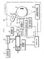
- FIG. 1 One form or embodiment for practicing the method of the present invention is illustrated in FIG. 1 which illustrates apparatus arranged within and around a chamber 30 which is either an vacuum chamber capable of maintaining a vacuum, or a housing divided into vacuum portions.
- a chamber 30 which is either an vacuum chamber capable of maintaining a vacuum, or a housing divided into vacuum portions.
- a movable support in the form of a movable support 31, a dielectric or monomer deposit system 32, a monomer curing system 33, and an optional metal material deposit system 34.
- a substantial vacuum is required, down to the order of 1 X 10 ⁇ 5 Torr.
- Movable support 31 is a water cooled drum 35 driven by a motor 36 whose outer cylindrical surface 37 defines a rapidly moving continuous surface passing through a dielectric or polymer layer forming zone and an optional metal forming zone.
- the regions in which the drum surface 37 and the systems 32, 33 are located constitute the dielectric or polymer layer forming zone, and the region in which the drum surface 37 and the system 34 are located constitute a metal forming zone.
- Drum rotation creates the machine direction 26, which is the direction the surface or support passes through the upstream dielectric forming zone and the downstream metal forming zone.
- the surface 37 should be smooth and true.
- a sheet or substrate 13 of a flexible material is firmly secured to the drum 35 and, when in place, the outer surface of the substrate defines the surface 37.
- the drum 35 is cooled to a temperature specific to the particular monomer being used and generally in the range of 20°C to 80°C to facilitate condensation of the vapor deposits, and the apparatus functions at drum surface speeds of 1 to 1000 cm/second.
- the optional metal/inorganic material deposit system 34 includes a conventional electron beam vaporization device 41 or a group of resistive evaporation sources (boats) such as those used for metallizing film within a vacuum environment or a sputtering target.
- the rate of vaporization can be sensed by a quartz monitoring device 42 providing feedback for controlling the rate at which aluminum is vaporized by the device 41.
- the pattern in which aluminum vapor is deposited can be controlled by a mask, in this case a shadow mask 43, having openings through which the vapor passes.
- the dielectric deposit system 32 flash vaporizes a dielectric in monomer form, and the smaller gaseous molecules are guided under moderate differential pressure through nozzles 64 onto the surface 37 of substrate 13.
- the monomeric materials employed in the process should provide an average of about two or more olefinic groups per molecule.
- a single diolefinic material, mixtures of two diolefins, or mixtures containing a polyolefin and a monolefin can be employed. If multiple components are utilized, the components can be metered into an evaporator individually or as a single mixture.
- the monomers (or monomer mixtures) utilized are highly reactive. As a result, the monomers can be deposited and cured at rapid speeds, viz, 1 to 1000 cm/sec.
- polyfunctional acrylates are particularly useful monomeric materials.
- the general formula for such polyfunctional acrylates is: wherein: R1 is an aliphatic, alicyclic or mixed aliphatic-alicyclic radical derived from a compound of the formula R1(OH) m ; R2 is hydrogen, methyl, ethyl, propyl, butyl or pentyl; n is from 2 to 4; m is 2 or more.
- Such polyfunctional acrylates may also be used in combination with various monoacrylates, such as those having the formula: wherein: R2, r and 2 are defined above; x1 is H or: X3 is CN or COOR3 wherein R3 is an alkyl radical containing 1-4 carbon atoms. Most often, X3 is CN or COOCH3.
- Diacrylates of the formula below are particularly preferred: wherein: r and s are each 7 or 8 and the sum of r and s is 15.
- the diacrylates and alkoxylated cyclohexane dimethanol diacrylates (wherein the alkoxy group contains 1 to 4 carbon atoms) are especially suitable.
- the monomer in liquid form is fed through a line 57 and control valve 56 to the open end of the horn 58 of an ultrasonic atomizer 59.
- the resulting micro droplets impinge on the inner walls of a vaporization tube 61 heated by band heaters 62 to an appropriate temperature, approximately 100- 400°C. for the acrylate resins referred to above.
- the liquid is thus instantaneously vaporized, i.e., flash vaporized, so as to minimize the opportunity for polymerization prior to being deposited on the substrate.
- Pressure in the tube 61 causes a monomer gas stream to flow through nozzles 55 for deposition and condensation.
- the nozzles 55 are heated by conduction from the tube 61 to minimize condensation before the gas stream leaves the nozzles.
- the thickness of the monomeric coating is dependent upon the time of deposit, i.e., the length of the nozzles 55 relative to the speed of the surface 37, and the rate of monomer flow through the valve 57.
- FIG. 6 An alternate arrangement for atomizing the liquid monomer is suggested in FIG. 6 wherein the monomer is directed through a capillary tube 68 to a point closely adjacent the horn 58 of the ultrasonic atomizer 59.
- a meniscus is formed between the end of the capillary tube 68 and the end of the horn 58, and the monomer is drawn uniformly through the tube.
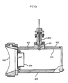
- FIG. 62 Another system which is preferred for atomizing the liquid monomer is shown in FIG. 62 in which monomer is directed through capillary tube 200 to a point closely adjacent ultrasonic atomizer 201.
- the monomer droplets are atomized ultrasonically and the droplets vaporized by the means of heating elements 203, 204 which heat the walls of atomization chamber 205.
- the vaporized monomer passes through a top hat shaped baffle 206, screen 207 and nozzle 208, where it condenses on the movable support, now shown.
- Nozzle 208 is shaped to conform substantially to the shape of the surface of the movable drum.
- the condensed liquid monomer is radiation cured by the second system 33 in the dielectric forming zone which includes a radiation source, preferably a gas discharge electron beam gun 70.
- the gun 70 directs a flow of electrons from a housing chamber 71 through an emitter window 72 onto the monomer, thereby curing the material to a polymerized cross linked form capable of withstanding high temperatures. Curing is controlled by matching the electron beam voltage to the dielectric thickness. For example, a 10 Kv electron voltage will penetrate about 1 micron of deposited monomer.
- the gun 70 includes a rectangular copper cathode 73 supported by a connector 74 in an insulator 75 mounted in a ground shield 76 that is fixed to the housing 71.
- a tungsten mesh extraction screen 77 is fixed across the window 72.
- a gas such as argon is fed to the housing chamber 71 through a line 78 and a control valve 79.
- An electrical potential is imposed between the cathode 73 and its connector 74, and the shield 76, housing 71 and screen 77, with the result, keeping in mind the vacuum environment, that a gaseous plasma is created in the housing, primarily between the cathode 73 and the screen 77.
- the cathode is preferably formed with grooves 81 on its face so that electrons are expelled in a non-linear beam to substantially fill the housing chamber 71. Because of the plasma created, other electrons are stripped from the ionized gas molecules in different portions of the chamber, a so-called field enhanced effect, with the result that electrons at widely varying energy levels are emitted from the window 72. The wide range of energy levels of the emitted electrons is believed to cause the observed effect that the monomer is cured with little surface charging.
- Other types of electronic guns i.e., thermionic guns
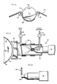
- FIG. 2 illustrates a second, preferred embodiment of apparatus which can be employed in the method of the present invention.
- a movable support in the form of a rotatable drum 100 having a cooled surface 101 driven by a motor, not shown.
- a liquid monomer delivery, metering and deposit system 102, a monomer curing system 104, and a metal or inorganic material deposit system 106 are also shown.
- the movable drum support 100, the vapor outlet of the monomer flash vaporizer, the curing means and optional inorganic material deposit apparatus 106 are disposed within the vacuum environment.
- Drum 100 continuously rotates the cooled drum surface 101 through an upstream polymer layer forming zone.
- the region in which surface 101 passes the monomer condensation and downstream curing systems 102, 104 constitutes the polymer layer forming zone, whereas the region in which the drum surface 101 passes the inorganic material deposit system 106 constitutes the inorganic or metal forming zone.
- Deposit system 106 is optional. If desired, inorganic material deposit system 106 could be eliminated if a single layer of organic coating is all that is desired. Alternatively, system 106 could be replaced by a second liquid monomer delivery, metering and deposit system (not shown) similar to system 102. This second monomer system could be used to deposit a second layer of the same or different monomer mixture on the substrate, if desired.
- a liquid monomer at room temperature is deposited in reservoir 112 where it passes to a deareator 113 where the monomer is stirred and degased at a temperature of about 25°C by pulling a vacuum to remove gases entrained in the monomer to preclude, insofar as possible, any pressure variation in the monomer evaporator.
- the monomer then passes through valve 114 to a conventional piston pump 116 which pumps the monomer under suitable pressure and temperature to a monomer metering means 118 which meters a desired amount of monomer to ultrasonic atomizer 120 through constricted conduit 121 which provides a positive back pressure for the monomer entering atomizer 120.
- the monomer is atomized and forms micro droplets which are heated to an appropriate temperature, approximately 100-400°C. for the acrylate resins referred to above.
- the droplets are instantaneously vaporized, i.e., flash vaporized, in evaporator 122 to minimize the opportunity for polymerization and the vaporized monomer condenses on the cooled drum surface 101.
- a flow rate of the monomer through the constriction 121 generally in the range 0.5 to 10 cc/min. has been found satisfactory with the flow rate being dependent upon the speed of the movable support, the desired layer thickness, and the width of the deposit.
- the monomer is metered in order that the amount of monomer entering atomizer 120 will be the optimum amount deposited on the movable support. It is important that the metered monomer material is deposited on the movable support, otherwise the monomer will polymerize on the walls of the evaporator.
- the condensed monomer liquid is subsequently radiation cured in the polymer or dielectric forming zone which includes a radiation source, preferably a gas discharge electron beam gun 124.
- a radiation source preferably a gas discharge electron beam gun 124.
- gun 124 in the manner previously described for the electron beam gun system of FIG. 1, causes a flow of electrons to be directed onto the monomer, thereby curing the material to a polymerized cross linked form.
- the gun is positioned to be aligned tangentially to the drum surface 101 in order that the flow of electrons contact the monomer tangentially as opposed to the 90° angle disclosed in FIG. 1. It has been found that by positioning the gun in the manner described for the embodiment of FIG. 2, the surface charge is reduced, charging defects are eliminated, and a more uniform cure from the top to the bottom of the monomer layer is achieved.
- An inorganic metal deposition system 126 is provided which is similar to the mask retraction and shifting system shown in FIG. 1, which comprises a controller 50, mask shifting motor 47, mask retractor motor 51 and removable shutter 52.
- a controller 128 is connected to the drum motor, not shown, for sensing drum revolution. Controller 128 serves to provide the appropriate signals to the monomer delivery system, flash vaporization retractor 130, which positions the vaporizer the desired distance relative to the drum surface, and the electron beam curing system for activating the curing system. The controller 128 can also supply the appropriate shifting to the mask retraction and shifting means, if a mask is employed.
- the rotatable drum shown in FIGS. 1 and 2 can be replaced with other types of movable supports.
- a rotatable disk 160 which could serve as a movable support with a cured adherent film 162 being formed on the surface of the disk.
- a disk 164 which is adapted to be rotated continuously or indexed intermittently at a desired speed, past deposition and curing stations heretofore described, to provide a number of coated substrates 166, 168.
- FIG. 4c shows a movable support which comprises a reciprocating plate 170 having a substrate 172 attached to a cooled surface 173. A cured monomer film 174 has been deposited on substrate 173.
- FIG. 4d shows a rotatable drum 176 with a water cooled surface 177.
- a moving web substrate passes over rollers 178, 179, the rollers serving to maintain the moving substrate in contact with the drum surface so that it can be cooled by the drum. While the substrate is in contact with the drum surface, a monomer coating 180 can be applied to the moving substrate and cured.
Landscapes
- Engineering & Computer Science (AREA)
- Chemical & Material Sciences (AREA)
- Power Engineering (AREA)
- Wood Science & Technology (AREA)
- Manufacturing & Machinery (AREA)
- Metallurgy (AREA)
- Organic Chemistry (AREA)
- Life Sciences & Earth Sciences (AREA)
- Materials Engineering (AREA)
- Chemical Kinetics & Catalysis (AREA)
- Mechanical Engineering (AREA)
- Microelectronics & Electronic Packaging (AREA)
- Health & Medical Sciences (AREA)
- General Health & Medical Sciences (AREA)
- Toxicology (AREA)
- Physics & Mathematics (AREA)
- Plasma & Fusion (AREA)
- Physical Vapour Deposition (AREA)
Applications Claiming Priority (2)
| Application Number | Priority Date | Filing Date | Title |
|---|---|---|---|
| US07/188,036 US4842893A (en) | 1983-12-19 | 1988-04-29 | High speed process for coating substrates |
| US188036 | 1998-11-06 |
Publications (2)
| Publication Number | Publication Date |
|---|---|
| EP0340935A2 true EP0340935A2 (de) | 1989-11-08 |
| EP0340935A3 EP0340935A3 (de) | 1991-01-16 |
Family
ID=22691525
Family Applications (1)
| Application Number | Title | Priority Date | Filing Date |
|---|---|---|---|
| EP19890303754 Withdrawn EP0340935A3 (de) | 1988-04-29 | 1989-04-17 | Schnellaufendes Verfahren zur Beschichtung von Substraten |
Country Status (3)
| Country | Link |
|---|---|
| US (1) | US4842893A (de) |
| EP (1) | EP0340935A3 (de) |
| JP (1) | JPH01316450A (de) |
Cited By (35)
| Publication number | Priority date | Publication date | Assignee | Title |
|---|---|---|---|---|
| EP0390540A3 (de) * | 1989-03-30 | 1991-12-27 | Sharp Kabushiki Kaisha | Herstellungsverfahren einer Dünnschicht aus organischem Material für eine optische Vorrichtung |
| WO1996031571A1 (en) * | 1995-04-06 | 1996-10-10 | Catalina Coatings, Inc. | RELEASE COATING, OBTAINED BY VAPOR DEPOSITION OF FLUORINATED OR SILICONE ACRYLATE COMPOUND, AND METHOD OF PRODUCTION THEREOf |
| WO1996031649A1 (en) * | 1995-04-06 | 1996-10-10 | Catalina Coatings, Inc. | Acrylate polymer coated sheet materials and method of production thereof |
| WO2000024558A1 (en) * | 1998-10-28 | 2000-05-04 | Matsushita Electric Industrial Co., Ltd. | Method of producing thin resin films |
| WO2000035604A1 (en) * | 1998-12-16 | 2000-06-22 | Battelle Memorial Institute | Plasma enhanced polymer deposition onto fixtures |
| WO2000035606A1 (en) * | 1998-12-16 | 2000-06-22 | Battelle Memorial Institute | Method of making non-linear optical polymer |
| WO2000035605A1 (en) * | 1998-12-16 | 2000-06-22 | Battelle Memorial Institute | Conformal coating of a microtextured surface |
| WO2000035602A1 (en) * | 1998-12-16 | 2000-06-22 | Battelle Memorial Institute | Plasma enhanced chemical deposition of conjugated polymer |
| WO2000035603A1 (en) * | 1998-12-16 | 2000-06-22 | Battelle Memorial Institute | Plasma enhanced chemical deposition for high and/or low index of refraction polymers |
| EP0938971A3 (de) * | 1998-02-27 | 2001-01-24 | Matsushita Electric Industrial Co., Ltd. | Verfahren zur Herstellung eines Mehrschichtstoffes |
| US6224948B1 (en) | 1997-09-29 | 2001-05-01 | Battelle Memorial Institute | Plasma enhanced chemical deposition with low vapor pressure compounds |
| US6228436B1 (en) | 1998-12-16 | 2001-05-08 | Battelle Memorial Institute | Method of making light emitting polymer composite material |
| US6268695B1 (en) | 1998-12-16 | 2001-07-31 | Battelle Memorial Institute | Environmental barrier material for organic light emitting device and method of making |
| WO2001066481A1 (fr) | 2000-03-08 | 2001-09-13 | Saint-Gobain Glass France | Substrat transparent revetu d'une couche polymere |
| US6358570B1 (en) | 1999-03-31 | 2002-03-19 | Battelle Memorial Institute | Vacuum deposition and curing of oligomers and resins |
| US6413645B1 (en) | 2000-04-20 | 2002-07-02 | Battelle Memorial Institute | Ultrabarrier substrates |
| US6492026B1 (en) | 2000-04-20 | 2002-12-10 | Battelle Memorial Institute | Smoothing and barrier layers on high Tg substrates |
| US6506461B2 (en) | 1999-03-31 | 2003-01-14 | Battelle Memorial Institute | Methods for making polyurethanes as thin films |
| US6548912B1 (en) | 1999-10-25 | 2003-04-15 | Battelle Memorial Institute | Semicoductor passivation using barrier coatings |
| US6570325B2 (en) | 1998-12-16 | 2003-05-27 | Battelle Memorial Institute | Environmental barrier material for organic light emitting device and method of making |
| US6573652B1 (en) | 1999-10-25 | 2003-06-03 | Battelle Memorial Institute | Encapsulated display devices |
| US6623861B2 (en) | 2001-04-16 | 2003-09-23 | Battelle Memorial Institute | Multilayer plastic substrates |
| US6866901B2 (en) | 1999-10-25 | 2005-03-15 | Vitex Systems, Inc. | Method for edge sealing barrier films |
| US7186465B2 (en) | 1998-11-02 | 2007-03-06 | 3M Innovative Properties Company | Transparent conductive oxides for plastic flat panel displays |
| US7510913B2 (en) | 2003-04-11 | 2009-03-31 | Vitex Systems, Inc. | Method of making an encapsulated plasma sensitive device |
| EP2073249A1 (de) * | 2007-12-21 | 2009-06-24 | Applied Materials, Inc. | Lineare Elektronenquelle, die lineare Elektronenquelle verwendender Verdampfer und Anwendungen von Elektronenquellen |
| US7648925B2 (en) | 2003-04-11 | 2010-01-19 | Vitex Systems, Inc. | Multilayer barrier stacks and methods of making multilayer barrier stacks |
| US7727601B2 (en) | 1999-10-25 | 2010-06-01 | Vitex Systems, Inc. | Method for edge sealing barrier films |
| US7767498B2 (en) | 2005-08-25 | 2010-08-03 | Vitex Systems, Inc. | Encapsulated devices and method of making |
| US8590338B2 (en) | 2009-12-31 | 2013-11-26 | Samsung Mobile Display Co., Ltd. | Evaporator with internal restriction |
| US8900366B2 (en) | 2002-04-15 | 2014-12-02 | Samsung Display Co., Ltd. | Apparatus for depositing a multilayer coating on discrete sheets |
| US9184410B2 (en) | 2008-12-22 | 2015-11-10 | Samsung Display Co., Ltd. | Encapsulated white OLEDs having enhanced optical output |
| US9337446B2 (en) | 2008-12-22 | 2016-05-10 | Samsung Display Co., Ltd. | Encapsulated RGB OLEDs having enhanced optical output |
| US9822454B2 (en) | 2006-12-28 | 2017-11-21 | 3M Innovative Properties Company | Nucleation layer for thin film metal layer formation |
| US9839940B2 (en) | 2002-04-15 | 2017-12-12 | Samsung Display Co., Ltd. | Apparatus for depositing a multilayer coating on discrete sheets |
Families Citing this family (211)
| Publication number | Priority date | Publication date | Assignee | Title |
|---|---|---|---|---|
| EP0420596B1 (de) * | 1989-09-26 | 1996-06-19 | Canon Kabushiki Kaisha | Gasversorgungsvorrichtung und ihre Verwendung für eine Filmabscheidungsanlage |
| US5204314A (en) * | 1990-07-06 | 1993-04-20 | Advanced Technology Materials, Inc. | Method for delivering an involatile reagent in vapor form to a CVD reactor |
| US5711816A (en) * | 1990-07-06 | 1998-01-27 | Advanced Technolgy Materials, Inc. | Source reagent liquid delivery apparatus, and chemical vapor deposition system comprising same |
| US7323581B1 (en) | 1990-07-06 | 2008-01-29 | Advanced Technology Materials, Inc. | Source reagent compositions and method for forming metal films on a substrate by chemical vapor deposition |
| US5362328A (en) * | 1990-07-06 | 1994-11-08 | Advanced Technology Materials, Inc. | Apparatus and method for delivering reagents in vapor form to a CVD reactor, incorporating a cleaning subsystem |
| JP3393135B2 (ja) * | 1991-12-13 | 2003-04-07 | アドバンスド テクノロジィ マテリアルズ,インコーポレイテッド | 不揮発性反応物を送り出す装置及び方法 |
| US5260095A (en) * | 1992-08-21 | 1993-11-09 | Battelle Memorial Institute | Vacuum deposition and curing of liquid monomers |
| GB2280864B (en) * | 1993-08-13 | 1996-09-25 | Komfort Systems Ltd | Method of coating elongate aluminium sections |
| US5814367A (en) * | 1993-08-13 | 1998-09-29 | General Atomics | Broadband infrared and signature control materials and methods of producing the same |
| US6033782A (en) * | 1993-08-13 | 2000-03-07 | General Atomics | Low volume lightweight magnetodielectric materials |
| ATE233939T1 (de) | 1993-10-04 | 2003-03-15 | 3M Innovative Properties Co | Vernetztes acrylatbeschichtungsmaterial zur herstellung von kondensatordielektrika und sauerstoffbarrieren |
| US20040241454A1 (en) * | 1993-10-04 | 2004-12-02 | Shaw David G. | Barrier sheet and method of making same |
| US5440446A (en) * | 1993-10-04 | 1995-08-08 | Catalina Coatings, Inc. | Acrylate coating material |
| US5803976A (en) * | 1993-11-09 | 1998-09-08 | Imperial Chemical Industries Plc | Vacuum web coating |
| US5464710A (en) * | 1993-12-10 | 1995-11-07 | Deposition Technologies, Inc. | Enhancement of optically variable images |
| DE69518710T2 (de) | 1994-09-27 | 2001-05-23 | Applied Materials Inc | Verfahren zum Behandeln eines Substrats in einer Vakuumbehandlungskammer |
| US5545375A (en) * | 1994-10-03 | 1996-08-13 | Becton, Dickinson And Company | Blood collection tube assembly |
| US5614259A (en) * | 1994-10-14 | 1997-03-25 | Deposition Technologies, Inc. | Microwave interactive susceptors and methods of producing the same |
| US6083628A (en) | 1994-11-04 | 2000-07-04 | Sigma Laboratories Of Arizona, Inc. | Hybrid polymer film |
| US6235105B1 (en) | 1994-12-06 | 2001-05-22 | General Atomics | Thin film pigmented optical coating compositions |
| US5681615A (en) * | 1995-07-27 | 1997-10-28 | Battelle Memorial Institute | Vacuum flash evaporated polymer composites |
| US5683771A (en) * | 1996-01-30 | 1997-11-04 | Becton, Dickinson And Company | Blood collection tube assembly |
| US5955161A (en) | 1996-01-30 | 1999-09-21 | Becton Dickinson And Company | Blood collection tube assembly |
| US5738920A (en) * | 1996-01-30 | 1998-04-14 | Becton, Dickinson And Company | Blood collection tube assembly |
| US5686157A (en) * | 1996-01-30 | 1997-11-11 | Becton, Dickinson And Company | Blood collection tube assembly |
| US5716683A (en) * | 1996-01-30 | 1998-02-10 | Becton, Dickinson And Company | Blood collection tube assembly |
| US5702770A (en) * | 1996-01-30 | 1997-12-30 | Becton, Dickinson And Company | Method for plasma processing |
| US5763033A (en) | 1996-01-30 | 1998-06-09 | Becton, Dickinson And Company | Blood collection tube assembly |
| US5731948A (en) * | 1996-04-04 | 1998-03-24 | Sigma Labs Inc. | High energy density capacitor |
| MY143286A (en) * | 1996-05-21 | 2011-04-15 | Panasonic Corp | Thin film, method and apparatus for forming the same, and electronic component incorporating the same |
| KR19980033213A (ko) * | 1996-10-31 | 1998-07-25 | 조셉제이.스위니 | 스퍼터링 챔버내의 미립자 물질 발생 감소 방법 |
| US5719417A (en) * | 1996-11-27 | 1998-02-17 | Advanced Technology Materials, Inc. | Ferroelectric integrated circuit structure |
| US5876503A (en) * | 1996-11-27 | 1999-03-02 | Advanced Technology Materials, Inc. | Multiple vaporizer reagent supply system for chemical vapor deposition utilizing dissimilar precursor compositions |
| US5895531A (en) * | 1996-12-13 | 1999-04-20 | Compuvac Systems, Inc. | Apparatus and polymerization gun for coating objects by vacuum deposit |
| US5912069A (en) * | 1996-12-19 | 1999-06-15 | Sigma Laboratories Of Arizona | Metal nanolaminate composite |
| US5882416A (en) * | 1997-06-19 | 1999-03-16 | Advanced Technology Materials, Inc. | Liquid delivery system, heater apparatus for liquid delivery system, and vaporizer |
| US5923970A (en) * | 1997-11-20 | 1999-07-13 | Advanced Technology Materials, Inc. | Method of fabricating a ferrolelectric capacitor with a graded barrier layer structure |
| US6045864A (en) * | 1997-12-01 | 2000-04-04 | 3M Innovative Properties Company | Vapor coating method |
| US6012647A (en) * | 1997-12-01 | 2000-01-11 | 3M Innovative Properties Company | Apparatus and method of atomizing and vaporizing |
| US5970908A (en) * | 1997-12-13 | 1999-10-26 | Compuvac Systems, Inc. | Apparatus and improved polymerization gun for coating objects by vacuum deposit |
| US6030671A (en) * | 1998-01-09 | 2000-02-29 | Msc Specialty Films, Inc. | Low emissivity window films |
| US6309508B1 (en) * | 1998-01-15 | 2001-10-30 | 3M Innovative Properties Company | Spinning disk evaporator |
| US5904958A (en) * | 1998-03-20 | 1999-05-18 | Rexam Industries Corp. | Adjustable nozzle for evaporation or organic monomers |
| US6251334B1 (en) * | 1998-03-23 | 2001-06-26 | Presstek, Inc. | Composite constructions having mixed organic/inorganic layers |
| EP0984859B1 (de) | 1998-03-23 | 2003-05-28 | Presstek, Inc. | Lithographisches verfahren mit anorganisch-organischen mischungen enthaltenden schichten |
| US6146462A (en) * | 1998-05-08 | 2000-11-14 | Astenjohnson, Inc. | Structures and components thereof having a desired surface characteristic together with methods and apparatuses for producing the same |
| US6105501A (en) * | 1998-06-10 | 2000-08-22 | Flex Products, Inc. | High resolution lithographic printing plate suitable for imaging with laser-discharge article and method |
| US6232365B1 (en) | 1998-07-17 | 2001-05-15 | 3M Innovative Properties Company | Low temperature electron beam polymerization |
| US6146225A (en) * | 1998-07-30 | 2000-11-14 | Agilent Technologies, Inc. | Transparent, flexible permeability barrier for organic electroluminescent devices |
| US6863851B2 (en) * | 1998-10-23 | 2005-03-08 | Avery Dennison Corporation | Process for making angstrom scale and high aspect functional platelets |
| US20030178734A1 (en) * | 1998-10-23 | 2003-09-25 | Karl Josephy | Process for making angstrom scale and high aspect functional platelets |
| ES2212645T3 (es) | 1998-10-23 | 2004-07-16 | Avery Dennison Corporation | Procedimiento para la fabricacion de laminillas metalicas. |
| US6503564B1 (en) * | 1999-02-26 | 2003-01-07 | 3M Innovative Properties Company | Method of coating microstructured substrates with polymeric layer(s), allowing preservation of surface feature profile |
| US6172810B1 (en) | 1999-02-26 | 2001-01-09 | 3M Innovative Properties Company | Retroreflective articles having polymer multilayer reflective coatings |
| AU6931200A (en) | 1999-08-24 | 2001-03-19 | Procter & Gamble Company, The | Durably wettable liquid pervious webs prepared using a radiation curing process |
| US6322665B1 (en) | 1999-10-25 | 2001-11-27 | Kimberly-Clark Corporation | Reactive compounds to fibrous webs |
| US6264791B1 (en) | 1999-10-25 | 2001-07-24 | Kimberly-Clark Worldwide, Inc. | Flash curing of fibrous webs treated with polymeric reactive compounds |
| US20100330748A1 (en) | 1999-10-25 | 2010-12-30 | Xi Chu | Method of encapsulating an environmentally sensitive device |
| US6521324B1 (en) | 1999-11-30 | 2003-02-18 | 3M Innovative Properties Company | Thermal transfer of microstructured layers |
| DE19960465A1 (de) * | 1999-12-15 | 2001-06-21 | Alcatel Sa | Flachleiter-Bandleitung |
| WO2001045930A1 (fr) * | 1999-12-22 | 2001-06-28 | Toray Industries, Inc. | Film multicouche et son procede de fabrication |
| US6237529B1 (en) * | 2000-03-03 | 2001-05-29 | Eastman Kodak Company | Source for thermal physical vapor deposition of organic electroluminescent layers |
| WO2002004552A1 (en) * | 2000-07-06 | 2002-01-17 | Commonwealth Scientific And Industrial Research Organisation | A process for modifying the surface of a substrate containing a polymeric material by means of vaporising the surface modifying agent |
| AUPQ859000A0 (en) * | 2000-07-06 | 2000-07-27 | Commonwealth Scientific And Industrial Research Organisation | Apparatus for surface engineering |
| US7195797B2 (en) * | 2000-07-10 | 2007-03-27 | Atomic Telecom | High throughput high-yield vacuum deposition system |
| US20030072689A1 (en) * | 2001-08-15 | 2003-04-17 | Third Wave Technologies, Inc. | Polymer synthesizer |
| US6706449B2 (en) | 2000-12-21 | 2004-03-16 | Moltech Corporation | Lithium anodes for electrochemical cells |
| US6468595B1 (en) * | 2001-02-13 | 2002-10-22 | Sigma Technologies International, Inc. | Vaccum deposition of cationic polymer systems |
| US6802315B2 (en) | 2001-03-21 | 2004-10-12 | Hollingsorth & Vose Company | Vapor deposition treated electret filter media |
| US6612356B2 (en) | 2001-04-10 | 2003-09-02 | Exxonmobil Oil Corporation | Apparatus for improving film machinability during film sealing |
| WO2002091064A2 (en) * | 2001-05-04 | 2002-11-14 | General Atomics | O2 and h2o barrier material |
| US20030031802A1 (en) * | 2001-05-11 | 2003-02-13 | 3M Innovative Properties Company | Pulsed electron beam polymerization |
| US6888305B2 (en) * | 2001-11-06 | 2005-05-03 | Universal Display Corporation | Encapsulation structure that acts as a multilayer mirror |
| US6597111B2 (en) | 2001-11-27 | 2003-07-22 | Universal Display Corporation | Protected organic optoelectronic devices |
| US6765351B2 (en) * | 2001-12-20 | 2004-07-20 | The Trustees Of Princeton University | Organic optoelectronic device structures |
| US7012363B2 (en) * | 2002-01-10 | 2006-03-14 | Universal Display Corporation | OLEDs having increased external electroluminescence quantum efficiencies |
| US20030157000A1 (en) * | 2002-02-15 | 2003-08-21 | Kimberly-Clark Worldwide, Inc. | Fluidized bed activated by excimer plasma and materials produced therefrom |
| US7112351B2 (en) * | 2002-02-26 | 2006-09-26 | Sion Power Corporation | Methods and apparatus for vacuum thin film deposition |
| US6897474B2 (en) * | 2002-04-12 | 2005-05-24 | Universal Display Corporation | Protected organic electronic devices and methods for making the same |
| US6835950B2 (en) | 2002-04-12 | 2004-12-28 | Universal Display Corporation | Organic electronic devices with pressure sensitive adhesive layer |
| US20090041936A1 (en) * | 2002-06-26 | 2009-02-12 | Sigma Laboratories Of Arizona, Llc. | Composite reflective barrier |
| US20040028931A1 (en) * | 2002-06-26 | 2004-02-12 | Bletsos Ioannis V. | Coated sheet materials and packages made therewith |
| EP1717018B1 (de) * | 2002-06-26 | 2009-04-01 | E.I. du Pont de Nemours and Company | Beschichtete Faserstoffbahn |
| DE60226718D1 (de) * | 2002-07-08 | 2008-07-03 | Galileo Vacuum Systems S R L | Vorrichtung zur chargenweisen Vakuumbeschichtung von Gegenständen |
| US6929864B2 (en) * | 2002-08-17 | 2005-08-16 | 3M Innovative Properties Company | Extensible, visible light-transmissive and infrared-reflective film and methods of making and using the film |
| US6818291B2 (en) * | 2002-08-17 | 2004-11-16 | 3M Innovative Properties Company | Durable transparent EMI shielding film |
| US6933051B2 (en) * | 2002-08-17 | 2005-08-23 | 3M Innovative Properties Company | Flexible electrically conductive film |
| US7215473B2 (en) * | 2002-08-17 | 2007-05-08 | 3M Innovative Properties Company | Enhanced heat mirror films |
| US6994933B1 (en) | 2002-09-16 | 2006-02-07 | Oak Ridge Micro-Energy, Inc. | Long life thin film battery and method therefor |
| CN1176565C (zh) * | 2002-11-25 | 2004-11-17 | 清华大学 | 一种有机电致发光器件的封装层及其制备方法和应用 |
| US20040180162A1 (en) * | 2003-03-14 | 2004-09-16 | Gringoire Bruno R.L. | Reduced blocking metallized film |
| US6797397B1 (en) * | 2003-03-20 | 2004-09-28 | Exxonmobil Oil Corporation | Lamination structure with a starch to plastic bond |
| US7018713B2 (en) * | 2003-04-02 | 2006-03-28 | 3M Innovative Properties Company | Flexible high-temperature ultrabarrier |
| US20040202708A1 (en) * | 2003-04-14 | 2004-10-14 | 3M Innovative Properties Company | Transdermal drug delivery device with translucent inorganic barrier layer |
| US7051282B2 (en) * | 2003-06-13 | 2006-05-23 | Microsoft Corporation | Multi-layer graphical user interface |
| US7052772B2 (en) * | 2003-08-14 | 2006-05-30 | 3M Innovative Properties Company | Material for packaging electronic components |
| US6998648B2 (en) * | 2003-08-25 | 2006-02-14 | Universal Display Corporation | Protected organic electronic device structures incorporating pressure sensitive adhesive and desiccant |
| US7140741B2 (en) * | 2003-12-30 | 2006-11-28 | 3M Innovative Properties Company | Color shifting retroreflector and method of making same |
| EP1771257A4 (de) * | 2004-05-27 | 2009-10-21 | Sigma Lab Arizona Inc | Grossflächige elektrolumineszente lichtemittierende vorrichtungen |
| US20050269943A1 (en) * | 2004-06-04 | 2005-12-08 | Michael Hack | Protected organic electronic devices and methods for making the same |
| US20060040091A1 (en) * | 2004-08-23 | 2006-02-23 | Bletsos Ioannis V | Breathable low-emissivity metalized sheets |
| CN100526917C (zh) * | 2004-12-28 | 2009-08-12 | 3M创新有限公司 | 具有含氟或含硅的棱镜的棱镜式逆向反射制品 |
| US7195360B2 (en) * | 2004-12-28 | 2007-03-27 | 3M Innovative Properties Company | Prismatic retroreflective article and method |
| US20060141244A1 (en) * | 2004-12-29 | 2006-06-29 | Toray Industries, Inc. | Multilayer film and process for producing the same |
| US20060153997A1 (en) * | 2005-01-07 | 2006-07-13 | Eastman Kodak Company | Method of varying wavelengths of liquid crystals |
| US20070020451A1 (en) * | 2005-07-20 | 2007-01-25 | 3M Innovative Properties Company | Moisture barrier coatings |
| US8658248B2 (en) * | 2005-12-29 | 2014-02-25 | 3M Innovative Properties Company | Method for atomizing material for coating processes |
| US8323801B2 (en) * | 2006-01-18 | 2012-12-04 | E I Du Pont De Nemours And Company | Process for forming a durable low emissivity moisture vapor permeable metallized sheet including a protective metal oxide layer |
| US8417474B2 (en) * | 2006-02-10 | 2013-04-09 | The Procter & Gamble Company | Methods of use of substrate having properties of keratinous tissue |
| JP4954574B2 (ja) * | 2006-03-02 | 2012-06-20 | 日東電工株式会社 | 透明ガスバリア性フィルムの製造方法および透明ガスバリア性フィルムの製造装置 |
| US20100136865A1 (en) * | 2006-04-06 | 2010-06-03 | Bletsos Ioannis V | Nonwoven web of polymer-coated nanofibers |
| CN101460555B (zh) * | 2006-06-05 | 2013-12-11 | 亨凯尔公司 | 用于塑料膜和金属箔基材的可甑馏的辐射固化涂层 |
| US20080006819A1 (en) * | 2006-06-19 | 2008-01-10 | 3M Innovative Properties Company | Moisture barrier coatings for organic light emitting diode devices |
| BRPI0715565A2 (pt) | 2006-10-19 | 2013-07-02 | Univ Arkansas Board Of Regents | mÉtodos e aparelho para fazer revestimentos usando pulverizaÇço eletrostÁtica |
| MX349614B (es) * | 2006-10-19 | 2017-07-26 | Nanomech Inc | Metodos y aparatos para elaborar recubrimientos utilizando deposicion de rocio ultrasonico. |
| US8120854B2 (en) * | 2006-12-28 | 2012-02-21 | 3M Innovative Properties Company | Interference films having acrylamide layer and method of making same |
| CN101573471A (zh) * | 2006-12-29 | 2009-11-04 | 3M创新有限公司 | 固化含有金属烷氧化物的膜的方法 |
| BRPI0720867A2 (pt) * | 2006-12-29 | 2014-03-04 | 3M Innovative Properties Company. | Método para fabricação de filmes inorgânicos ou híbridos inorgânicos/orgânicos |
| US8084102B2 (en) * | 2007-02-06 | 2011-12-27 | Sion Power Corporation | Methods for co-flash evaporation of polymerizable monomers and non-polymerizable carrier solvent/salt mixtures/solutions |
| JP4922148B2 (ja) * | 2007-02-15 | 2012-04-25 | 富士フイルム株式会社 | バリア性積層体、バリア性フィルム基板、それらの製造方法、およびデバイス |
| EP1958981B1 (de) | 2007-02-15 | 2018-04-25 | FUJIFILM Corporation | Sperrschichtlaminat, sperrfoliensubstrat, herstellungsverfahren dafür und vorrichtung |
| JP4995137B2 (ja) | 2007-06-11 | 2012-08-08 | 富士フイルム株式会社 | ガスバリアフィルムおよびこれを用いた有機デバイス |
| US20090015142A1 (en) * | 2007-07-13 | 2009-01-15 | 3M Innovative Properties Company | Light extraction film for organic light emitting diode display devices |
| US8179034B2 (en) * | 2007-07-13 | 2012-05-15 | 3M Innovative Properties Company | Light extraction film for organic light emitting diode display and lighting devices |
| JP2009028949A (ja) | 2007-07-25 | 2009-02-12 | Fujifilm Corp | バリア性フィルム基板とその製造方法、および有機デバイス |
| US8586189B2 (en) | 2007-09-19 | 2013-11-19 | Fujifilm Corporation | Gas-barrier film and organic device comprising same |
| CN101939669A (zh) * | 2007-10-30 | 2011-01-05 | 3M创新有限公司 | 用于光学显示滤光片的带电磁干扰屏蔽的多层堆叠光学带通膜 |
| US20090162667A1 (en) * | 2007-12-20 | 2009-06-25 | Lumination Llc | Lighting device having backlighting, illumination and display applications |
| EP2231395A4 (de) * | 2007-12-28 | 2014-01-29 | 3M Innovative Properties Co | Infrarotreflektierende filme für solarsteuerung und andere verwendungen |
| BRPI0819548A2 (pt) * | 2007-12-28 | 2015-05-19 | 3M Innovative Properties Co | "sistemas de filme de encapsulação flexível" |
| JP5255856B2 (ja) | 2008-01-31 | 2013-08-07 | 富士フイルム株式会社 | 機能性フィルムの製造方法 |
| JP4536784B2 (ja) | 2008-01-31 | 2010-09-01 | 富士フイルム株式会社 | 機能性フィルムの製造方法 |
| JP4912344B2 (ja) | 2008-03-21 | 2012-04-11 | 富士フイルム株式会社 | バリア性積層体とその製造方法、バリア性フィルム基板、デバイスおよび光学部材 |
| JP5081712B2 (ja) * | 2008-05-02 | 2012-11-28 | 富士フイルム株式会社 | 成膜装置 |
| US8350451B2 (en) * | 2008-06-05 | 2013-01-08 | 3M Innovative Properties Company | Ultrathin transparent EMI shielding film comprising a polymer basecoat and crosslinked polymer transparent dielectric layer |
| US9481927B2 (en) * | 2008-06-30 | 2016-11-01 | 3M Innovative Properties Company | Method of making inorganic or inorganic/organic hybrid barrier films |
| US20100110551A1 (en) * | 2008-10-31 | 2010-05-06 | 3M Innovative Properties Company | Light extraction film with high index backfill layer and passivation layer |
| EP2358529A4 (de) * | 2008-11-17 | 2013-08-28 | 3M Innovative Properties Co | Barriere mit gradientenförmiger zusammensetzung |
| JP5658452B2 (ja) | 2008-12-16 | 2015-01-28 | 富士フイルム株式会社 | 積層体の製造方法 |
| US7957621B2 (en) * | 2008-12-17 | 2011-06-07 | 3M Innovative Properties Company | Light extraction film with nanoparticle coatings |
| US9464179B2 (en) | 2009-04-15 | 2016-10-11 | 3M Innovative Properties Company | Process and apparatus for a nanovoided article |
| US9291752B2 (en) | 2013-08-19 | 2016-03-22 | 3M Innovative Properties Company | Retroreflecting optical construction |
| TWI491930B (zh) | 2009-04-15 | 2015-07-11 | 3M新設資產公司 | 光學膜 |
| JP5671003B2 (ja) | 2009-04-15 | 2015-02-18 | スリーエム イノベイティブ プロパティズ カンパニー | ナノ中空物品用プロセス及び装置 |
| BRPI1006654A2 (pt) | 2009-04-15 | 2016-02-10 | 3M Innovative Properties Co | construções ópticas retrorrefletoras e filmes ópticos |
| CN102474999B (zh) | 2009-08-03 | 2016-09-07 | 3M创新有限公司 | 用于形成光学透明的导电金属或金属合金薄膜的方法以及由其制成的膜 |
| US9472783B2 (en) * | 2009-10-12 | 2016-10-18 | General Electric Company | Barrier coating with reduced process time |
| JP5341704B2 (ja) * | 2009-10-15 | 2013-11-13 | 小島プレス工業株式会社 | 積層シートの製造装置及び製造方法 |
| JP5940980B2 (ja) | 2009-11-18 | 2016-06-29 | スリーエム イノベイティブ プロパティズ カンパニー | 多層光学フィルム |
| US10544502B2 (en) | 2009-11-30 | 2020-01-28 | Xefco Pty Ltd | Functional composite garment materials |
| WO2011068695A1 (en) * | 2009-12-02 | 2011-06-09 | 3M Innovative Properties Company | Multilayer emi shielding thin film with high rf permeability |
| EP2558289B1 (de) | 2010-04-15 | 2018-12-26 | 3M Innovative Properties Company | Rückstrahlende artikel mit optisch aktiven bereichen und optisch inaktiven bereichen |
| WO2011129831A1 (en) | 2010-04-15 | 2011-10-20 | 3M Innovative Properties Company | Retroreflective articles including optically active areas and optically inactive areas |
| US9618663B2 (en) | 2010-04-15 | 2017-04-11 | 3M Innovative Properties Company | Retroreflective articles including optically active areas and optically inactive areas |
| US9254506B2 (en) | 2010-07-02 | 2016-02-09 | 3M Innovative Properties Company | Moisture resistant coating for barrier films |
| EP2588314B1 (de) | 2010-07-02 | 2020-08-19 | 3M Innovative Properties Company | Sperranordnung mit verkapselung und photovoltaischer zelle |
| JP5595190B2 (ja) | 2010-08-31 | 2014-09-24 | 富士フイルム株式会社 | 機能性フィルムおよび機能性フィルムの製造方法 |
| JP6247533B2 (ja) | 2010-10-06 | 2017-12-13 | スリーエム イノベイティブ プロパティズ カンパニー | ナノシリカ系コーティング及びバリア層を有する反射防止物品 |
| WO2012047422A1 (en) | 2010-10-06 | 2012-04-12 | 3M Innovative Properties Company | Anti-reflective articles with nanosilica-based coatings |
| JP5560208B2 (ja) * | 2011-01-06 | 2014-07-23 | 株式会社アルバック | 基板の接着方法及び基板積層体の製造方法 |
| WO2013019695A2 (en) | 2011-08-04 | 2013-02-07 | 3M Innovative Properties Company | Edge protected barrier assemblies |
| BR112014002320A2 (pt) * | 2011-08-05 | 2017-03-01 | 3M Innovative Properties Co | sistemas e métodos para processar vapor |
| US9777365B2 (en) | 2011-11-29 | 2017-10-03 | Itn Energy Systems, Inc. | Multi-zone modular coater |
| US9165717B1 (en) * | 2012-02-01 | 2015-10-20 | Sigma Laboratories Of Arizona, Llc | High-Surface Capacitor Electrode |
| US11058161B2 (en) | 2012-02-16 | 2021-07-13 | Xefco Pty Ltd | Heat reflecting composites with knitted insulation |
| US20150114297A1 (en) * | 2012-06-08 | 2015-04-30 | Sharp Kabushiki Kaisha | Vapor deposition device |
| SG11201500934RA (en) | 2012-08-08 | 2015-03-30 | 3M Innovative Properties Co | Barrier film constructions and methods of making same |
| TWI610806B (zh) | 2012-08-08 | 2018-01-11 | 3M新設資產公司 | 障壁膜,製造該障壁膜之方法,及包含該障壁膜之物件 |
| WO2014025383A1 (en) | 2012-08-08 | 2014-02-13 | 3M Innovative Properties Company | Photovoltaic devices with encapsulating barrier film |
| JP6268175B2 (ja) | 2012-08-08 | 2018-01-24 | スリーエム イノベイティブ プロパティズ カンパニー | 尿素(マルチ)−(メタ)アクリレート(マルチ)−シラン化合物及びそれを含む物品 |
| US10784455B2 (en) | 2012-08-08 | 2020-09-22 | 3M Innovative Properties Company | Coatings for barrier films and methods of making and using the same |
| WO2014081918A2 (en) | 2012-11-21 | 2014-05-30 | 3M Innovative Properties Company | Multilayer film including first and second dielectric layers |
| CN104903982B (zh) | 2012-11-21 | 2018-08-17 | 3M创新有限公司 | 包括第一介电层和第二介电层的多层膜 |
| JP6632378B2 (ja) | 2012-12-20 | 2020-01-22 | スリーエム イノベイティブ プロパティズ カンパニー | 紫外線吸収基を有するオリゴマーを含むフルオロポリマー組成物 |
| EP2935373A4 (de) | 2012-12-20 | 2016-07-27 | 3M Innovative Properties Co | Copolymere mit ultraviolettlicht-absorbierenden gruppen und fluorpolymerzusammensetzungen damit |
| US10160184B2 (en) | 2013-06-03 | 2018-12-25 | Xefco Pty Ltd | Insulated radiant barriers in apparel |
| WO2015013225A1 (en) | 2013-07-24 | 2015-01-29 | 3M Innovative Properties Company | Adhesive barrier film construction |
| WO2015047572A1 (en) | 2013-09-24 | 2015-04-02 | 3M Innovative Properties Company | Transferable transparent conductive patterns and display stack materials |
| JP6656154B2 (ja) | 2013-12-19 | 2020-03-04 | スリーエム イノベイティブ プロパティズ カンパニー | バリアフィルム及びバリアフィルムを用いる真空断熱パネル |
| WO2015200669A1 (en) | 2014-06-25 | 2015-12-30 | 3M Innovative Properties Company | Pressure sensitive adhesive composition including ultraviolet light-absorbing oligomer |
| US11110689B2 (en) | 2014-06-25 | 2021-09-07 | 3M Innovative Properties Company | Pressure sensitive adhesive composition including ultraviolet light-absorbing oligomer |
| JP6294513B2 (ja) | 2014-06-25 | 2018-03-14 | スリーエム イノベイティブ プロパティズ カンパニー | 少なくとも1つのオリゴマーを含むフルオロポリマー組成物 |
| EP3313906B1 (de) | 2015-06-25 | 2020-08-05 | 3M Innovative Properties Company | Copolymer mit gruppe, die ultraviolettes licht absorbiert, und zusammensetzungen damit |
| CN107922805B (zh) | 2015-08-17 | 2020-09-15 | 3M创新有限公司 | 纳米粘土填充的阻挡粘合剂组合物 |
| US10581015B2 (en) | 2015-08-17 | 2020-03-03 | 3M Innovative Properties Company | Barrier film constructions |
| WO2017031294A1 (en) | 2015-08-19 | 2017-02-23 | 3M Innovative Properties Company | Composite article including a multilayer barrier assembly and methods of making the same |
| US11584113B2 (en) | 2015-08-19 | 2023-02-21 | 3M Innovative Properties Company | Composite article including a multilayer barrier assembly and methods of making the same |
| KR101909426B1 (ko) | 2015-08-19 | 2018-10-17 | 쓰리엠 이노베이티브 프로퍼티즈 캄파니 | 복합 물품 및 그의 제조 방법 |
| CN108698369B (zh) | 2016-03-04 | 2021-03-09 | 3M创新有限公司 | 磁性多层片材 |
| WO2017165522A1 (en) | 2016-03-25 | 2017-09-28 | 3M Innovative Properties Company | Multilayer barrier films |
| US11034865B2 (en) | 2016-06-16 | 2021-06-15 | 3M Innovative Properties Company | Nanoparticle filled barrier adhesive compositions |
| KR102406867B1 (ko) | 2016-06-16 | 2022-06-13 | 쓰리엠 이노베이티브 프로퍼티즈 컴파니 | 나노입자 충전된 배리어 접착제 조성물 |
| JP2018063989A (ja) | 2016-10-11 | 2018-04-19 | Tdk株式会社 | 薄膜キャパシタ |
| JP6805702B2 (ja) | 2016-10-11 | 2020-12-23 | Tdk株式会社 | 薄膜コンデンサ |
| JP6737118B2 (ja) | 2016-10-11 | 2020-08-05 | Tdk株式会社 | 薄膜コンデンサ |
| US10756306B2 (en) | 2016-10-28 | 2020-08-25 | 3M Innovative Properties Company | Nanostructured article |
| US20200123419A1 (en) | 2017-04-21 | 2020-04-23 | 3M Innovative Properties Company | Barrier adhesive compositions and articles |
| CN111465669B (zh) | 2017-12-06 | 2022-12-16 | 3M创新有限公司 | 阻隔性粘合剂组合物和制品 |
| DE102018215102A1 (de) * | 2018-05-28 | 2019-11-28 | Sms Group Gmbh | Vakuumbeschichtungsanlage, und Verfahren zum Beschichten eines bandförmigen Materials |
| EP4150404A4 (de) | 2020-05-14 | 2024-05-29 | 3M Innovative Properties Company | Fluorierte photoinitiatoren und damit hergestellte fluorierte (co)polymerschichten |
| EP4150011B1 (de) | 2020-05-14 | 2026-06-24 | 3M Innovative Properties Company | Fluorierte kupplungsmittel und damit hergestellte fluorierte (co)polymerschichten |
| CN115701282A (zh) | 2020-05-14 | 2023-02-07 | 3M创新有限公司 | 包含至少一个使用氟化光引发剂制备的氟化(共)聚合物层的多层光学膜及其制备和使用方法 |
| US20240023350A1 (en) | 2020-12-09 | 2024-01-18 | 3M Innovative Properties Company | Barrier assembly for solar cells |
| US12157941B2 (en) | 2021-05-17 | 2024-12-03 | 3M Innovative Properties Company | Ultraviolet radiation and atomic oxygen barrier films and methods of making and using the same |
| EP4341086A1 (de) | 2021-05-19 | 2024-03-27 | 3M Innovative Properties Company | Verpackte schleifartikel |
| WO2022243772A1 (en) | 2021-05-20 | 2022-11-24 | 3M Innovative Properties Company | Micro-cut patterned article and method of making same |
| DE112023003019T5 (de) * | 2022-07-11 | 2025-05-22 | Rubycon Corporation | Dünnschichtpolymerlaminierter kondensator und herstellungsverfahren für diesen |
| EP4619797A1 (de) | 2022-11-17 | 2025-09-24 | 3M Innovative Properties Company | Strukturierte ultraviolettlichtabschirmungsartikel und solaranordnungen damit |
| US12666753B2 (en) | 2023-03-24 | 2026-06-23 | 3M Innovative Properties Company | Ultraviolet light shielding articles and solar cell covers including the same |
| WO2025037210A1 (en) | 2023-08-11 | 2025-02-20 | 3M Innovative Properties Company | Packaged abrasive articles |
| CN120174330A (zh) * | 2025-05-20 | 2025-06-20 | 合肥东昇智能装备股份有限公司 | 一种复合薄膜成形生产设备及其生产方法 |
Family Cites Families (64)
| Publication number | Priority date | Publication date | Assignee | Title |
|---|---|---|---|---|
| CA789746A (en) * | 1968-07-09 | General Electric Company | Electrical capacitor | |
| BE660489A (de) * | ||||
| BE516556A (de) * | ||||
| US1873548A (en) * | 1930-01-29 | 1932-08-23 | Aerovox Wireless Corp | Condenser |
| GB550419A (en) * | 1941-07-01 | 1943-01-07 | William Dubilier | Improvements in or relating to electrical condensers and the manufacture thereof |
| US2389420A (en) * | 1943-10-04 | 1945-11-20 | Du Pont | Manufacture of capacttors |
| US2614524A (en) * | 1946-08-22 | 1952-10-21 | Rca Corp | Capacitor manufacturing evaporation apparatus |
| US2590906A (en) * | 1946-11-22 | 1952-04-01 | Farrand Optical Co Inc | Reflection interference filter |
| BE520401A (de) * | 1952-06-03 | |||
| CH313676A (de) * | 1952-07-26 | 1956-04-30 | Bosch Gmbh Robert | Elektrischer Kondensator |
| US2820934A (en) * | 1954-08-18 | 1958-01-21 | Acf Ind Inc | Capacitor assembly |
| US3081201A (en) * | 1957-05-15 | 1963-03-12 | Gen Electric | Method of forming an electric capacitor |
| US3024394A (en) * | 1958-01-27 | 1962-03-06 | Zenith Radio Corp | Low inductance condenser |
| US3252830A (en) * | 1958-03-05 | 1966-05-24 | Gen Electric | Electric capacitor and method for making the same |
| GB970865A (en) * | 1959-12-14 | 1964-09-23 | Philco Corp | Improvements in and relating to electrical capacitors |
| US3068510A (en) * | 1959-12-14 | 1962-12-18 | Radiation Res Corp | Polymerizing method and apparatus |
| NL277968A (de) * | 1961-05-04 | |||
| US3237273A (en) * | 1962-08-17 | 1966-03-01 | Sangamo Electric Co | Method of making a capacitor |
| US3326718A (en) * | 1963-12-30 | 1967-06-20 | Hughes Aircraft Co | Method for making an electrical capacitor |
| US3457614A (en) * | 1964-09-29 | 1969-07-29 | Gen Instrument Corp | Process and apparatus for making thin film capacitors |
| FR1466995A (fr) * | 1965-02-04 | 1967-01-20 | Continental Can Co | Appareil et procédé pour condenser des vapeurs de monomères pour une polymérisation dans une décharge électrique |
| US3244953A (en) * | 1965-02-08 | 1966-04-05 | Erie Technological Prod Inc | Wound capacitor having hermetically sealed terminals |
| GB1104172A (en) * | 1965-03-30 | 1968-02-21 | Metal Containers Ltd | Glow discharge polymerization process |
| GB1168641A (en) * | 1966-05-19 | 1969-10-29 | British Iron Steel Research | Formation of Polymer Coatings on Substrates. |
| US3466719A (en) * | 1967-01-11 | 1969-09-16 | Texas Instruments Inc | Method of fabricating thin film capacitors |
| US3520987A (en) * | 1968-08-05 | 1970-07-21 | Eldre Components | High capacity bus bar |
| GB1253124A (de) * | 1969-02-28 | 1971-11-10 | ||
| US3743532A (en) * | 1969-12-29 | 1973-07-03 | Gen Electric | Coated substrate formed from photopolymerized gas |
| US3654532A (en) * | 1970-05-25 | 1972-04-04 | Illinois Tool Works | Multilayer plastic chip capacitor |
| US3617834A (en) * | 1970-08-31 | 1971-11-02 | Illinois Tool Works | Monolithic capacitor components and process for producing same |
| JPS4870855A (de) * | 1971-12-29 | 1973-09-26 | ||
| US4076866A (en) * | 1975-03-30 | 1978-02-28 | Massachusetts Institute Of Technology | Method of growing films by flash vaporization |
| JPS52113379A (en) * | 1976-03-19 | 1977-09-22 | Hitachi Ltd | Vacuum evaporation |
| DE2641232C2 (de) * | 1976-09-14 | 1982-10-21 | Robert Bosch Gmbh, 7000 Stuttgart | Schichtaufbau und Verfahren zu seiner Herstellung |
| FR2379889A1 (fr) * | 1977-02-08 | 1978-09-01 | Thomson Csf | Dielectrique constitue par un polymere en couche mince, procede de fabrication de ladite couche, et condensateurs electriques comportant un tel dielectrique |
| US4301580A (en) * | 1977-04-16 | 1981-11-24 | Wallace Clarence L | Manufacture of multi-layered electrical assemblies |
| US4207836A (en) * | 1977-07-01 | 1980-06-17 | Hitachi, Ltd. | Vacuum vapor-deposition apparatus |
| DE2737509A1 (de) * | 1977-08-19 | 1979-03-01 | Gilbert James Elderbaum | Verfahren zur herstellung von keramik-kondensatoren |
| DE2759118A1 (de) * | 1977-12-30 | 1979-07-12 | Siemens Ag | Verfahren zur herstellung eines stapelkondensators |
| JPS5527455A (en) * | 1978-08-17 | 1980-02-27 | Mitsubishi Electric Corp | Riveting method |
| DE2843581C2 (de) * | 1978-10-05 | 1986-03-27 | Siemens AG, 1000 Berlin und 8000 München | Elektrischer Schichtkondensator und Verfahren zu seiner Herstellung |
| DE2847620C2 (de) * | 1978-11-02 | 1984-10-18 | Siemens AG, 1000 Berlin und 8000 München | Vorrichtung zur Herstellung von elektrischen Bauelementen, insbesondere Schichtkondensatoren |
| US4301765A (en) * | 1979-01-10 | 1981-11-24 | Siemens Aktiengesellschaft | Apparatus for generating layers on a carrier foil |
| CA1129876A (en) * | 1979-01-10 | 1982-08-17 | Richard G. Palmer | Method of purifying readily polymerisable vinyl monomers |
| DE2900772C2 (de) * | 1979-01-10 | 1984-08-30 | Siemens AG, 1000 Berlin und 8000 München | Verfahren zur Erzeugung von Schichten auf einer bandförmigen Trägerfolie |
| DE2908467A1 (de) * | 1979-03-05 | 1980-09-11 | Siemens Ag | Regenerierfaehiger elektrischer schichtkondensator |
| DE2940337A1 (de) * | 1979-10-04 | 1981-04-09 | Siemens AG, 1000 Berlin und 8000 München | Verfahren zur herstellung von schichtkondensatoren |
| US4290384A (en) * | 1979-10-18 | 1981-09-22 | The Perkin-Elmer Corporation | Coating apparatus |
| JPS56101732A (en) * | 1980-01-18 | 1981-08-14 | Matsushita Electric Industrial Co Ltd | Metallized film condenser |
| DE3017507C2 (de) * | 1980-05-07 | 1982-06-03 | Siemens AG, 1000 Berlin und 8000 München | Verfahren zur Herstellung von Schichtkondensatoren |
| DE3021786A1 (de) * | 1980-06-10 | 1981-12-17 | Siemens AG, 1000 Berlin und 8000 München | Verfahren zur herstelung von elektrishen bauelementen, insbesondere schichtkondensatoren |
| DE3028123A1 (de) * | 1980-07-24 | 1982-02-25 | Siemens AG, 1000 Berlin und 8000 München | Verfahren und vorrichtung zur herstellung von schichtkondensatoren |
| WO1982000542A1 (en) * | 1980-08-04 | 1982-02-18 | Behn R | Device for making superposed metal layers and micaceous polymer layers,laterally off set relative to one another |
| US4329419A (en) * | 1980-09-03 | 1982-05-11 | E. I. Du Pont De Nemours And Company | Polymeric heat resistant photopolymerizable composition for semiconductors and capacitors |
| US4363162A (en) * | 1980-11-03 | 1982-12-14 | Price Rick A | Infrared heat treatment of plastic film capacitors |
| JPS57134558A (en) * | 1981-02-16 | 1982-08-19 | Fuji Photo Film Co Ltd | Production of organic vapor deposited thin film |
| DE3110351A1 (de) * | 1981-03-17 | 1982-09-30 | Siemens AG, 1000 Berlin und 8000 München | Verfahren zur herstellung von elektrischen schichtkondensatoren mit glimmpolymerisatschichten als dielektrika |
| JPS5874701A (ja) * | 1981-10-29 | 1983-05-06 | Sekisui Chem Co Ltd | 高分子薄膜の形成方法 |
| DE3231576A1 (de) * | 1982-08-25 | 1984-03-01 | Siemens AG, 1000 Berlin und 8000 München | Regenerierfaehiger elektrischer schichtkondensator |
| JPS59177365A (ja) * | 1983-03-24 | 1984-10-08 | Matsushita Electric Ind Co Ltd | 蒸発方法とその装置 |
| US4453199A (en) * | 1983-06-17 | 1984-06-05 | Avx Corporation | Low cost thin film capacitor |
| US4490774A (en) * | 1983-12-19 | 1984-12-25 | General Electric Company | Capacitors containing polyfunctional acrylate polymers as dielectrics |
| US4533710A (en) * | 1983-12-19 | 1985-08-06 | General Electric Company | 1,2-Alkanediol diacrylate monomers and polymers thereof useful as capacitor dielectrics |
| EP0147696B1 (de) * | 1983-12-19 | 1991-07-10 | SPECTRUM CONTROL, INC. (a Pennsylvania corporation) | Miniaturisierter monolithischer Mehrschichtkondensator sowie Gerät und Verfahren zur Herstellung |
-
1988
- 1988-04-29 US US07/188,036 patent/US4842893A/en not_active Expired - Lifetime
-
1989
- 1989-04-17 EP EP19890303754 patent/EP0340935A3/de not_active Withdrawn
- 1989-05-01 JP JP1113539A patent/JPH01316450A/ja active Pending
Cited By (70)
| Publication number | Priority date | Publication date | Assignee | Title |
|---|---|---|---|---|
| EP0390540A3 (de) * | 1989-03-30 | 1991-12-27 | Sharp Kabushiki Kaisha | Herstellungsverfahren einer Dünnschicht aus organischem Material für eine optische Vorrichtung |
| CN1095904C (zh) * | 1995-04-06 | 2002-12-11 | 普莱斯泰克公司 | 涂敷丙烯酸酯聚合物的板材及其生产方法 |
| WO1996031571A1 (en) * | 1995-04-06 | 1996-10-10 | Catalina Coatings, Inc. | RELEASE COATING, OBTAINED BY VAPOR DEPOSITION OF FLUORINATED OR SILICONE ACRYLATE COMPOUND, AND METHOD OF PRODUCTION THEREOf |
| WO1996031649A1 (en) * | 1995-04-06 | 1996-10-10 | Catalina Coatings, Inc. | Acrylate polymer coated sheet materials and method of production thereof |
| US5811183A (en) * | 1995-04-06 | 1998-09-22 | Shaw; David G. | Acrylate polymer release coated sheet materials and method of production thereof |
| US5945174A (en) * | 1995-04-06 | 1999-08-31 | Delta V Technologies, Inc. | Acrylate polymer release coated sheet materials and method of production thereof |
| AU709829B2 (en) * | 1995-04-06 | 1999-09-09 | 3M Innovative Properties Company | Acrylate polymer coated sheet materials and method of production thereof |
| US6218004B1 (en) | 1995-04-06 | 2001-04-17 | David G. Shaw | Acrylate polymer coated sheet materials and method of production thereof |
| KR100412777B1 (de) * | 1995-04-06 | 2005-05-03 | ||
| US6224948B1 (en) | 1997-09-29 | 2001-05-01 | Battelle Memorial Institute | Plasma enhanced chemical deposition with low vapor pressure compounds |
| US6656537B2 (en) | 1997-09-29 | 2003-12-02 | Battelle Memorial Institute | Plasma enhanced chemical deposition with low vapor pressure compounds |
| US6627267B2 (en) | 1997-09-29 | 2003-09-30 | Battelle Memorial Institute | Plasma enhanced chemical deposition with low vapor pressure compounds |
| EP0938971A3 (de) * | 1998-02-27 | 2001-01-24 | Matsushita Electric Industrial Co., Ltd. | Verfahren zur Herstellung eines Mehrschichtstoffes |
| CN1103685C (zh) * | 1998-02-27 | 2003-03-26 | 松下电器产业株式会社 | 层压体的制造方法 |
| US6270832B2 (en) | 1998-02-27 | 2001-08-07 | Matsushita Electric Industrial Co., Ltd. | Method for manufacturing a layered product |
| WO2000024558A1 (en) * | 1998-10-28 | 2000-05-04 | Matsushita Electric Industrial Co., Ltd. | Method of producing thin resin films |
| US6475571B1 (en) | 1998-10-28 | 2002-11-05 | Matsushita Electric Industrial Co., Ltd. | Method of producing thin resin films |
| US7186465B2 (en) | 1998-11-02 | 2007-03-06 | 3M Innovative Properties Company | Transparent conductive oxides for plastic flat panel displays |
| US7276291B2 (en) | 1998-11-02 | 2007-10-02 | 3M Innovative Properties Company | Transparent conductive articles and methods of making same |
| US6217947B1 (en) | 1998-12-16 | 2001-04-17 | Battelle Memorial Institute | Plasma enhanced polymer deposition onto fixtures |
| US6858259B2 (en) | 1998-12-16 | 2005-02-22 | Battelle Memorial Institute | Plasma enhanced chemical deposition for high and/or low index of refraction polymers |
| US6228436B1 (en) | 1998-12-16 | 2001-05-08 | Battelle Memorial Institute | Method of making light emitting polymer composite material |
| US6274204B1 (en) | 1998-12-16 | 2001-08-14 | Battelle Memorial Institute | Method of making non-linear optical polymer |
| WO2000035604A1 (en) * | 1998-12-16 | 2000-06-22 | Battelle Memorial Institute | Plasma enhanced polymer deposition onto fixtures |
| WO2000035606A1 (en) * | 1998-12-16 | 2000-06-22 | Battelle Memorial Institute | Method of making non-linear optical polymer |
| US6909230B2 (en) | 1998-12-16 | 2005-06-21 | Battelle Memorial Institute | Method of making molecularly doped composite polymer material |
| US6228434B1 (en) | 1998-12-16 | 2001-05-08 | Battelle Memorial Institute | Method of making a conformal coating of a microtextured surface |
| WO2000035605A1 (en) * | 1998-12-16 | 2000-06-22 | Battelle Memorial Institute | Conformal coating of a microtextured surface |
| US6207238B1 (en) | 1998-12-16 | 2001-03-27 | Battelle Memorial Institute | Plasma enhanced chemical deposition for high and/or low index of refraction polymers |
| US6497924B2 (en) | 1998-12-16 | 2002-12-24 | Battelle Memorial Institute | Method of making non-linear optical polymer |
| US6497598B2 (en) | 1998-12-16 | 2002-12-24 | Battelle Memorial Institute | Environmental barrier material for organic light emitting device and method of making |
| US6268695B1 (en) | 1998-12-16 | 2001-07-31 | Battelle Memorial Institute | Environmental barrier material for organic light emitting device and method of making |
| US6509065B2 (en) | 1998-12-16 | 2003-01-21 | Battelle Memorial Institute | Plasma enhanced chemical deposition of conjugated polymer |
| US6522067B1 (en) | 1998-12-16 | 2003-02-18 | Battelle Memorial Institute | Environmental barrier material for organic light emitting device and method of making |
| US6207239B1 (en) | 1998-12-16 | 2001-03-27 | Battelle Memorial Institute | Plasma enhanced chemical deposition of conjugated polymer |
| US6544600B2 (en) | 1998-12-16 | 2003-04-08 | Battelle Memorial Institute | Plasma enhanced chemical deposition of conjugated polymer |
| US6811829B2 (en) | 1998-12-16 | 2004-11-02 | Battelle Memorial Institute | Method of making a coating of a microtextured surface |
| US6570325B2 (en) | 1998-12-16 | 2003-05-27 | Battelle Memorial Institute | Environmental barrier material for organic light emitting device and method of making |
| WO2000035602A1 (en) * | 1998-12-16 | 2000-06-22 | Battelle Memorial Institute | Plasma enhanced chemical deposition of conjugated polymer |
| US6613395B2 (en) | 1998-12-16 | 2003-09-02 | Battelle Memorial Institute | Method of making molecularly doped composite polymer material |
| WO2000035603A1 (en) * | 1998-12-16 | 2000-06-22 | Battelle Memorial Institute | Plasma enhanced chemical deposition for high and/or low index of refraction polymers |
| US6506461B2 (en) | 1999-03-31 | 2003-01-14 | Battelle Memorial Institute | Methods for making polyurethanes as thin films |
| US6358570B1 (en) | 1999-03-31 | 2002-03-19 | Battelle Memorial Institute | Vacuum deposition and curing of oligomers and resins |
| USRE40531E1 (en) * | 1999-10-25 | 2008-10-07 | Battelle Memorial Institute | Ultrabarrier substrates |
| US6573652B1 (en) | 1999-10-25 | 2003-06-03 | Battelle Memorial Institute | Encapsulated display devices |
| US6548912B1 (en) | 1999-10-25 | 2003-04-15 | Battelle Memorial Institute | Semicoductor passivation using barrier coatings |
| US7727601B2 (en) | 1999-10-25 | 2010-06-01 | Vitex Systems, Inc. | Method for edge sealing barrier films |
| US6866901B2 (en) | 1999-10-25 | 2005-03-15 | Vitex Systems, Inc. | Method for edge sealing barrier films |
| USRE40787E1 (en) | 1999-10-25 | 2009-06-23 | Battelle Memorial Institute | Multilayer plastic substrates |
| US8955217B2 (en) | 1999-10-25 | 2015-02-17 | Samsung Display Co., Ltd. | Method for edge sealing barrier films |
| US6923702B2 (en) | 1999-10-25 | 2005-08-02 | Battelle Memorial Institute | Method of making encapsulated display devices |
| US6852393B2 (en) | 2000-03-08 | 2005-02-08 | Saint-Gobain Glass France | Transparent substrate coated with a polymer layer |
| WO2001066481A1 (fr) | 2000-03-08 | 2001-09-13 | Saint-Gobain Glass France | Substrat transparent revetu d'une couche polymere |
| US6413645B1 (en) | 2000-04-20 | 2002-07-02 | Battelle Memorial Institute | Ultrabarrier substrates |
| US6492026B1 (en) | 2000-04-20 | 2002-12-10 | Battelle Memorial Institute | Smoothing and barrier layers on high Tg substrates |
| US6623861B2 (en) | 2001-04-16 | 2003-09-23 | Battelle Memorial Institute | Multilayer plastic substrates |
| US8900366B2 (en) | 2002-04-15 | 2014-12-02 | Samsung Display Co., Ltd. | Apparatus for depositing a multilayer coating on discrete sheets |
| US9839940B2 (en) | 2002-04-15 | 2017-12-12 | Samsung Display Co., Ltd. | Apparatus for depositing a multilayer coating on discrete sheets |
| US7648925B2 (en) | 2003-04-11 | 2010-01-19 | Vitex Systems, Inc. | Multilayer barrier stacks and methods of making multilayer barrier stacks |
| US7510913B2 (en) | 2003-04-11 | 2009-03-31 | Vitex Systems, Inc. | Method of making an encapsulated plasma sensitive device |
| US7767498B2 (en) | 2005-08-25 | 2010-08-03 | Vitex Systems, Inc. | Encapsulated devices and method of making |
| US9822454B2 (en) | 2006-12-28 | 2017-11-21 | 3M Innovative Properties Company | Nucleation layer for thin film metal layer formation |
| WO2009080430A1 (en) * | 2007-12-21 | 2009-07-02 | Applied Materials, Inc. | Linear electron source, evaporator using linear electron source, and appliccations of electron sources |
| US7928411B2 (en) | 2007-12-21 | 2011-04-19 | Applied Materials, Inc. | Linear electron source, evaporator using linear electron source, and applications of electron sources |
| EP2073249A1 (de) * | 2007-12-21 | 2009-06-24 | Applied Materials, Inc. | Lineare Elektronenquelle, die lineare Elektronenquelle verwendender Verdampfer und Anwendungen von Elektronenquellen |
| US9337446B2 (en) | 2008-12-22 | 2016-05-10 | Samsung Display Co., Ltd. | Encapsulated RGB OLEDs having enhanced optical output |
| US9184410B2 (en) | 2008-12-22 | 2015-11-10 | Samsung Display Co., Ltd. | Encapsulated white OLEDs having enhanced optical output |
| US9362530B2 (en) | 2008-12-22 | 2016-06-07 | Samsung Display Co., Ltd. | Encapsulated white OLEDs having enhanced optical output |
| US8904819B2 (en) | 2009-12-31 | 2014-12-09 | Samsung Display Co., Ltd. | Evaporator with internal restriction |
| US8590338B2 (en) | 2009-12-31 | 2013-11-26 | Samsung Mobile Display Co., Ltd. | Evaporator with internal restriction |
Also Published As
| Publication number | Publication date |
|---|---|
| US4842893A (en) | 1989-06-27 |
| EP0340935A3 (de) | 1991-01-16 |
| JPH01316450A (ja) | 1989-12-21 |
Similar Documents
| Publication | Publication Date | Title |
|---|---|---|
| US4842893A (en) | High speed process for coating substrates | |
| US5032461A (en) | Method of making a multi-layered article | |
| JP2530350B2 (ja) | モノマ―流体のフラッシュ蒸発 | |
| US4954371A (en) | Flash evaporation of monomer fluids | |
| US4722515A (en) | Atomizing device for vaporization | |
| JP3560914B2 (ja) | 低蒸気圧化合物を用いたプラズマ加速化学蒸着 | |
| US20020076506A1 (en) | Plasma enhanced polymer deposition onto fixtures | |
| US6228434B1 (en) | Method of making a conformal coating of a microtextured surface | |
| EP1144131B1 (de) | Plasmaunterstützte gasphasenausscheidung von konjugierten polymeren | |
| JP2002532575A (ja) | 発光性高分子複合体を製造する方法 | |
| KR20010093841A (ko) | 고굴절률 중합체 및/또는 저굴절률 중합체용의 플라즈마증강 화학 증착법 | |
| US6475571B1 (en) | Method of producing thin resin films | |
| EP1035553B1 (de) | Verfahren zur herstellung von laminat | |
| EP1144135B1 (de) | Verfahren zum herstellen von polymeren mit nichtlinearen optischen eigenschaften | |
| EP0339844A2 (de) | Mehrschichtstruktur und Verfahren zu deren Herstellung | |
| CN104040017A (zh) | 直接液体淀积 | |
| Affinito et al. | Ultrahigh rate, wide area, plasma polymerized films from high molecular weight/low vapor pressure liquid or solid monomer precursors | |
| CN1285760C (zh) | 低蒸汽压化合物的等离子体增强化学沉积方法及其设备 | |
| Shaw et al. | Use of A New High Speed Acrylate Deposition Process to Make Novel Multilayer Structures | |
| JP2000195751A (ja) | 有機薄膜コンデンサ用積層シ―トの製造方法 | |
| MXPA00003090A (en) | Plasma enhanced chemical deposition with low vapor pressure compounds | |
| JPH0565627A (ja) | 蒸着重合装置 |
Legal Events
| Date | Code | Title | Description |
|---|---|---|---|
| PUAI | Public reference made under article 153(3) epc to a published international application that has entered the european phase |
Free format text: ORIGINAL CODE: 0009012 |
|
| AK | Designated contracting states |
Kind code of ref document: A2 Designated state(s): DE FR GB IT NL SE |
|
| PUAL | Search report despatched |
Free format text: ORIGINAL CODE: 0009013 |
|
| AK | Designated contracting states |
Kind code of ref document: A3 Designated state(s): DE FR GB IT NL SE |
|
| 17P | Request for examination filed |
Effective date: 19910711 |
|
| 17Q | First examination report despatched |
Effective date: 19920622 |
|
| STAA | Information on the status of an ep patent application or granted ep patent |
Free format text: STATUS: THE APPLICATION HAS BEEN WITHDRAWN |
|
| 18W | Application withdrawn |
Withdrawal date: 19921128 |