EP0341929B1 - Circuit multiplex - Google Patents
Circuit multiplex Download PDFInfo
- Publication number
- EP0341929B1 EP0341929B1 EP89304573A EP89304573A EP0341929B1 EP 0341929 B1 EP0341929 B1 EP 0341929B1 EP 89304573 A EP89304573 A EP 89304573A EP 89304573 A EP89304573 A EP 89304573A EP 0341929 B1 EP0341929 B1 EP 0341929B1
- Authority
- EP
- European Patent Office
- Prior art keywords
- path
- capacitors
- switching means
- channels
- devices
- Prior art date
- Legal status (The legal status is an assumption and is not a legal conclusion. Google has not performed a legal analysis and makes no representation as to the accuracy of the status listed.)
- Expired - Lifetime
Links
- 239000003990 capacitor Substances 0.000 claims abstract description 68
- 230000005669 field effect Effects 0.000 claims description 21
- 238000000151 deposition Methods 0.000 claims description 12
- 230000008021 deposition Effects 0.000 claims description 10
- 230000000694 effects Effects 0.000 claims description 10
- XUIMIQQOPSSXEZ-UHFFFAOYSA-N Silicon Chemical compound [Si] XUIMIQQOPSSXEZ-UHFFFAOYSA-N 0.000 claims description 9
- 229910052710 silicon Inorganic materials 0.000 claims description 9
- 239000010703 silicon Substances 0.000 claims description 9
- 238000007599 discharging Methods 0.000 claims description 5
- 230000001419 dependent effect Effects 0.000 claims description 4
- 239000007788 liquid Substances 0.000 claims description 4
- 239000011149 active material Substances 0.000 claims description 2
- 238000006073 displacement reaction Methods 0.000 claims description 2
- 108091006146 Channels Proteins 0.000 description 113
- 230000004913 activation Effects 0.000 description 2
- 238000010304 firing Methods 0.000 description 2
- 238000009877 rendering Methods 0.000 description 2
- 230000001154 acute effect Effects 0.000 description 1
- 239000000919 ceramic Substances 0.000 description 1
- 239000011248 coating agent Substances 0.000 description 1
- 238000000576 coating method Methods 0.000 description 1
- 238000010276 construction Methods 0.000 description 1
- 230000005288 electromagnetic effect Effects 0.000 description 1
- 239000012634 fragment Substances 0.000 description 1
- 238000010438 heat treatment Methods 0.000 description 1
- 230000000977 initiatory effect Effects 0.000 description 1
- 230000005855 radiation Effects 0.000 description 1
- 239000004065 semiconductor Substances 0.000 description 1
Images


Classifications
-
- B—PERFORMING OPERATIONS; TRANSPORTING
- B41—PRINTING; LINING MACHINES; TYPEWRITERS; STAMPS
- B41J—TYPEWRITERS; SELECTIVE PRINTING MECHANISMS, i.e. MECHANISMS PRINTING OTHERWISE THAN FROM A FORME; CORRECTION OF TYPOGRAPHICAL ERRORS
- B41J2/00—Typewriters or selective printing mechanisms characterised by the printing or marking process for which they are designed
- B41J2/005—Typewriters or selective printing mechanisms characterised by the printing or marking process for which they are designed characterised by bringing liquid or particles selectively into contact with a printing material
- B41J2/01—Ink jet
- B41J2/07—Ink jet characterised by jet control
- B41J2/075—Ink jet characterised by jet control for many-valued deflection
- B41J2/08—Ink jet characterised by jet control for many-valued deflection charge-control type
- B41J2/085—Charge means, e.g. electrodes
-
- B—PERFORMING OPERATIONS; TRANSPORTING
- B41—PRINTING; LINING MACHINES; TYPEWRITERS; STAMPS
- B41J—TYPEWRITERS; SELECTIVE PRINTING MECHANISMS, i.e. MECHANISMS PRINTING OTHERWISE THAN FROM A FORME; CORRECTION OF TYPOGRAPHICAL ERRORS
- B41J2202/00—Embodiments of or processes related to ink-jet or thermal heads
- B41J2202/01—Embodiments of or processes related to ink-jet heads
- B41J2202/10—Finger type piezoelectric elements
Definitions
- This invention relates to multiplexer circuits for effecting in successive phases of operation thereof actuation of selected devices of respective groups of devices of a series of capacitance actuated devices.
- a multiplexer circuit is a pulsed droplet deposition apparatus, such as a drop-on-demand ink jet printer having a multi-channel array from the channels of which the droplets are ejected and in which the channels are arranged in groups, channels from the respective groups being selected for printing droplets in successive phases of operation of the multiplexer circuit.
- a pulsed droplet deposition apparatus such as a drop-on-demand ink jet printer having a multi-channel array from the channels of which the droplets are ejected and in which the channels are arranged in groups, channels from the respective groups being selected for printing droplets in successive phases of operation of the multiplexer circuit.
- circuits to handle substantial actuating currents have to be constructed and such currents give rise to risk of burn-out failure.
- One object of the present invention is to provide a multiplexer circuit for such an application which is called upon to handle only relatively low power. Further, in known forms of pulsed droplet ink jet printer the switching of the substantial actuating currents gives rise to radio fre
- GB-A-2 104 005 discloses a circuit for operating a single capitance actuated device using two parallel electrical paths, each comprising first and second switching means.
- the present invention consists in a multiplexer circuit for effecting in successive phases of operation thereof actuation of selected devices of respective groups of devices of a series of capacitance actuated devices, characterised in that said circuit comprises a series of parallel connected electrical paths to which the respective devices are adapted to be connected, said paths being adapted for connection in parallel with a signal generator, with two capacitors of each device connected between the path of the associated device and the respective paths on opposite sides of said path of said associated device and first and second switching means disposed in each path and adapted to be closed by respective logic signals applied thereto so that when the first and second switching means of one path are respectively closed and open and the first and second switching means of each of the paths on respective opposite sides of said one path are respectively open and closed, charging of the capacitors connected to said one path takes place and when thereafter the first and second switching means of said one path are respectively open and closed discharge of the capacitors connected to said one path takes place.
- a diode device is connected across the second switching means of each path and provides a conductive path for discharging capacitors connected between the path in which said diode is connected and the paths on respective opposite sides thereof.
- the first and second switching means are provided on a silicon chip integrated circuit, said switching means comprising transistor switches.
- the transistor means comprise field effect transistors.
- the second switching means of each path comprises first and second switching components of which the first switching component provides a by-pass path in parallel with the second switching component during charging of the capacitors connected between the path containing said second switching means and the paths on opposite sides thereof by way of the first switching means of said paths on opposite sides of the path containing said second switching means, whilst the second switching component provides a conductive path for discharging the capacitors connected to the path containing said second switching component after charging thereof by way of the first switching means contained in the same path as said second switching component.
- the first and second switching means are provided on a silicon chip integrated circuit, the first switching means comprising a field effect transistor and the first and second switching components of the second switching means comprising respectively a field effect transistor and a field effect transistor controlling conduction of a bipolar transistor.
- the capacitors of devices selected for actuation are charged in an initial part of a voltage waveform-supplied from the signal generator after which the signal generator is disconnected from the circuit for a further interval of said waveform prior to discharge of the charged capacitors.
- the signal generator and the parallel electrical paths and the first and second switching means thereof are formed in a silicon chip integrated circuit.
- the logic signal applying means are adapted to apply signals to the first and second switching means to enable charging of the capacitors of each of the devices selected for actuation for a period dependent upon the actuated or non-actuated status of devices adjacent each of said selected devices.
- the invention further consists in a multi-channel array, electrically pulsed droplet deposition apparatus for depositing liquid droplets upon a surface, comprising a droplet deposition head formed from electrically active material, a multiplicity of channels for liquid formed in said head and arranged in a plurality of groups, nozzles communicating with the respective channels, longitudinal side walls each serving to divide one channel from the next and electrically actuable means for effecting transverse displacement in opposite senses of said longitudinal side-walls of each channel, said electrically actuable means comprising electrodes in each channel on respective facing surfaces of the longitudinal channel side-walls, conductive means connecting the electrodes in each channel, said electrodes forming a series of capacitors each consisting of one of said longitudinal channel side walls and the electrodes on opposite sides thereof and a multiplexer circuit for effecting in successive phases of operation actuation of said longitudinal walls of selected channels in the respective channel groups, said circuit comprising a series of parallel electrical paths, said capacitors being connected respectively between successive paths of said electrical paths, a signal generator connected across said parallel
- the logic signal applying means are adapted to apply signals to the first and second switching means in each of said parallel paths to which the capacitors of selected channels are connected to enable charging of the capacitors of each selected channel for a period to provide a voltage level thereon dependent upon the selected or non-selected status of adjacent channels of the group containing the selected channels.
- the signal generator is adapted during charging of said capacitors to apply a signal to the capacitors of the selected channels which is of relatively slowly increasing voltage and the logic signal applying means are adapted to effect disconnection of the signal generator from the capacitors of said selected channels when a predetermined charge voltage is reached and after an interval to actuate the switching means to effect rapid discharge of the charged capacitors whereby during charging of the capacitors of the selected channels the longitudinal side walls of the said channel are displaced outwardly relatively slowly and during discharge of the capacitors the channel walls are rapidly returned.
- Figure 1 illustrates a module part 10 of an ink jet printhead 12 in which a multiplicity of closely spaced drop-on-demand ink drop ejectors are disposed side by side in an array.
- the ejectors consist of extended parallel channels 20-28 filled with ink and separated by piezo-electric shear mode wall actuators 30-39, such as are disclosed in EP-A-0 278 590.
- the ink channels 20-28 have electrodes 40-48 coating the walls of each channel, which provide actuating electrodes for the wall actuators and which, together with the wall actuators effectively form capacitors 50 to 58.
- the electrodes are connected via tracks 70-78 to terminals 60-68 of a silicon chip integrated circuit hereinafter referred to.
- the ink ejectors are divided separately into two groups of odd and even numbered channels and selected channels in the odd and even numbered groups are actuated in alternating cycles.
- operation is performed by holding the electrodes of one group (e.g. the even numbered channels) at earth potential and applying a voltage waveform to those channels due to print in the odd group of channels.
- FIG. 2 shows a signal generator 100 provided in a silicon chip integrated circuit 101 and connected across internal buses 102 and 103 thereof, bus 102 being connected to the positive output terminal of the signal generator and bus 103 to the negative output terminal thereof which is held at ground potential. Between the buses 102 and 103, there are provided parallel electrical paths respectively associated with the actuator channels and of which only paths 113 to 117 are illustrated and these respectively include terminals 63 to 67.
- the paths 113 to 117 respectively include the collector emitter paths of n-p-n bipolar transistor devices 133 to 137.
- the base emitter paths of these devices respectively include field effect devices 143 to 147 to the gate electrodes of which are applicable internally generated logic signals to render these devices conductive.
- the collector emitter paths of devices 133 to 137 are shunted by respective field effect devices 153 to 157 the gate electrodes of which are connected to the gate electrodes of devices 143 to 147 so that these devices are rendered conductive by the same logic signals as activate the devices 143 to 147.
- the devices 153 to 157 are themselves respectively shunted by diodes 163 to 167 which provide capacitor discharge paths as hereinafter referred to.
- the logic signals for effecting and terminating conduction of the transistors 123-127, 143-147 and 153-157 are supplied from registers 173-177 of logic block 178 to which is supplied print pattern data on a line 179 and relatively high frequency clock pulses on a line 180 which connects also with the signal generator 100 to which is also connected a clock line 181 on which are supplied relatively low frequency clock pulses.
- the data stream supplied on line 179 consists of an N bit print pattern applied to each chip of the printhead where N is the number of channels to which the chip is connected.
- the N bits determine in one cycle which of the channels of the even numbered channel group are to be actuated and in a following cycle which of the channels of the odd numbered channel group are to be actuated.
- the N bit data stream additionally contains subsets n of data relating to the print status of channels of the same group as those selected for actuation on opposite sides of each of the selected channels which are to be actuated.
- the data sets n may be four bit words in which case they give the print status of two channels of the same group as the selected channels on each side of each channel selected for actuation. If the data sets n are in the form of six bit words they give the print status of three channels on each side of each channel which is to be actuated.
- the data N with its subsets n is loaded into the registers 173 to 177 at the rate set by the clock pulses on line 180, suitably about 10MHertz and the data sets n are sent to a look-up table in a ROM (not shown) which sends digital signals respectively determined by the data sets n to the registers 173-177 which signals are stored in the registers and employed to afford a count of pulses on line 180 which determines the level of charging of the capacitors of each actuated channel.
- the voltage cycles applied by the signal generator 100 across the buses 102 and 103 are initiated by the pulses on the clock line 181 and upon initiation of one such cycle the data stored in the registers 171 to 177 selects for printing the channels of one of the channel groups which have their transistors 123-127 switched on and their transistors 143 to 147 switched off so that charging of the capacitors of the selected channels commences and is terminated by switching off of the transistors 123-127 of the selected channels when the voltage level thereon reaches a value determined by the digital signals stored in the registers 173-179 and supplied thereto from the look-up table referred to.
- FIG 4 illustrates the waveform provided by the signal generator 100 to energise the actuators 30 to 39 during successive phases of the two phase multiplexer circuit circuit of Figure 2.
- the waveform consists of a charge period ⁇ 1 during which the charge on the capacitors 52 to 57 belonging to one of the channel groups gradually rises to predetermined values for each channel of that group selected for actuation at which the capacitors are disconnected from the signal generator and remain at or substantially at their charged voltage level for a further period, the "hold" period, ⁇ 2, during which the signal voltage is kept at least at the level of the charge voltage.
- the signal voltage is allowed in this period first to rise above and at the end of the period return to the charge voltage.
- the signal voltage proceeds to zero to enable reconnection of the signal generator to the capacitors for the next phase of operation. Before that commences a rapid discharge of the capacitors, as hereinafter described, is effected.
- the wall actuator electrodes of selected channels of say the odd numbered channels 21 to 27 are energised to cause the wall actuators to deform outwards from the channels into a chevron or cantilever form as described in the co-pending European patent application referred to due to the charge voltage and the direction of polarisation of the wall actuators.
- the rate of rise of voltage is however gradual so that the magnitude of the acoustic waves formed in the ink channels only mildly disturbs the ink menisci in the ejection nozzles of the channels and is not sufficient to eject drops of ink from the nozzles of the even numbered channels adjacent the activated even numbered channels.
- the charge period ⁇ 1 exceeds the time of travel of acoustic waves in the activated channels so that ⁇ 1 ⁇ L/C where L is the channel length and C is the acoustic wave velocity in the channels.
- the hold period ⁇ 2 further ink is drawn into the activated odd numbered channels by the action of the acoustic waves and this causes the channel wall actuators to relax outwardly as the ink quantity in the channels increases.
- the pressure of ink in the selected channels is a maximum and the capacitors of those channels are then rapidly discharged to cause rapid inward movement of the channel actuator walls which generates pressure waves in the selected channels causing ejection of an ink drop from the nozzles of those channels.
- the next phase of operation is effected on selected even numbered channels by a further signal phase of the signal generator.
- the capacitors 54 and 55 therefore, relatively slowly, charge to a predetermined voltage during the period ⁇ 1, by way of, in the case of capacitor 54, the field effect devices 125 and 154, and, in the case of capacitor 55, by way of field effect devices 125 and 156, the predetermined voltage being determined by the signal from the ROM stored in register 175.
- the actuator walls of channel 25 accordingly move outwards allowing flow of ink into that channel and, because of the slow rate of charge, no ink drops are expelled from the adjoining channels.
- the logic signals to the field effect devices 125 are removed so disconnecting the actuators from the drive circuit signal.
- Firing that is to say discharge of the capacitor 54 and 55 is effected by applying a signal from the register 175 after a predetermined count of pulses on line 180 to the gate electrodes of the field effect devices 145 and 155 rendering bipolar transistor 135 conducting.
- This establishes a discharge for capacitor 54 by way of transistor 135 and diode 164 and for capacitor 55 by way of transistor 135 and diode 166.
- both field effect devices 145 and 155 are conducting, because of the relative resistances of bi-polar transistor 135 and field effect device 155 most of the discharge current flows through transistor 135.
- capacitors 54 and 55 flow through transistor 135 and divide equally between diodes 164 and 166 and these relatively high discharge currents flow respectively in clockwise and anti-clockwise paths so that the electromagnetic effects thereof effectively cancel out thus minimising radio frequency interference.
- the heating effect of current in the circuit 101 is largely confined to the capacitor discharge currents and therefore to the turn on time of the bi-polar transistors which lasts, typically 30 n. seconds.
- discharge of capacitors 54 and 55 takes place in 2» seconds causing currents typically of the order of 100mA and resulting in rapid return of the actuator walls of channel 25 to their relaxed positions thereby developing ink drop ejection pressure in channel 25.
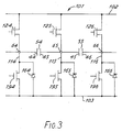
- Figure 3 shows a fragment of an alternative design of two phase multiplexer circuit to that of Figure 2 and which is of C-Mos design. It will be seen that in the parallel paths 114,115,116, the diodes now shunt respective field effect transistors 194,195,196. The requisite logic signals for effecting operation of the circuit are the same as for the circuit of Figure 2 and are not shown.
- devices 124 to 126 are in a non-conducting condition and devices 194 to 196 are held in a conducting state by a logic signal applied to their gate electrodes.
- capacitors 54 and 55 are charged during period ⁇ 1 by reason of a logic signal being applied to the gate electrode of field effect devices 125 from the associated register, such as register 175 of Figure 2 and the signal at the gate electrode of device 195 is removed.
- switch devices of the integrated circuit could include instead of field effect and bi-polar transistors, silicon controlled rectifiers, four layer diodes or other forms of semi-conductor switch devices.
Landscapes
- Electronic Switches (AREA)
- Particle Formation And Scattering Control In Inkjet Printers (AREA)
- Time-Division Multiplex Systems (AREA)
- Circuits Of Receivers In General (AREA)
- Ink Jet (AREA)
- Input Circuits Of Receivers And Coupling Of Receivers And Audio Equipment (AREA)
- Arrangements For Transmission Of Measured Signals (AREA)
Claims (17)
- Circuit multiplexeur pour effectuer la mise en oeuvre, lors de phases successives de fonctionnement de ce circuit, de dispositifs sélectionnés parmi des groupes respectifs de dispositifs d'une série de dispositifs mis en oeuvre par capacité (23 à 27), caractérisé en ce que ledit circuit comprend une série de trajets électriques parallèles reliés (113 à 117) auxquels les dispositifs respectifs (23 à 27) sont conçus pour être reliés, lesdits trajets étant conçus pour se connecter en parallèle à un générateur de signal (100), deux condensateurs (54, 55) de chaque dispositif (25) étant reliés entre le trajet du dispositif associé (115) et les trajets respectifs (114, 116) sur les côtés opposés dudit trajet dudit dispositif associé, et comprend un premier (125) et un second (135) moyens de commutation disposés dans chaque trajet (115) et conçus pour être fermés par des signaux logiques respectifs qui leur sont appliqués de façon que lorsque le premier (125) et le second (135) moyens de commutation d'un trajet (115) particulier sont respectivement fermé et ouvert et lorsque le premier (124, 126) et le second (134, 136) moyens de commutation de chacun des trajets (114, 116) sur les côtés opposés respectifs dudit trajet (115) particulier sont respectivement ouvert et fermé, il se produit la charge des condensateurs (54, 55) reliés audit trajet (115) particulier et lorsque, après cela, le premier (125) et le second (135) moyens de commutation dudit trajet (115) particulier sont respectivement ouvert et fermé, il se produit la décharge des condensateurs (54, 55) reliés audit trajet particulier.
- Circuit multiplexeur selon la revendication 1, caractérisé en ce que lesdits dispositifs (23 à 27) de ladite série de dispositifs sont agencés en deux groupes de dispositifs imbriqués.
- Circuit multiplexeur selon la revendication 2, caractérisé en ce que lesdits dispositifs (23 à 27) d'un premier desdits groupes alternent dans ladite série avec des dispositifs respectifs d'un second desdits groupes.
- Circuit selon l'une quelconque des revendications précédentes, caractérisé en ce qu'un dispositif à diode (165) est relié aux bornes du second moyen de commutation (135) de chaque trajet et réalise un trajet conducteur pour décharger les condensateurs (54, 55) reliés entre le trajet dans lequel ladite diode est connectée et les trajets sur les côtés opposés respectifs de ce dernier.
- Circuit selon l'une quelconque des revendications précédentes, caractérisé en ce que les premier et second moyens de commutation (125, 135) sont réalisés sur un circuit intégré à puces de silicium, lesdits moyens de commutation comprenant des commutateurs à transistors.
- Circuit selon la revendication 5, caractérisé en ce que les commutateurs à transistors comprennent des transistors à effet de champ (125, 195).
- Circuit selon l'une quelconque des revendications précédentes, caractérisé en ce que le second moyen de commutation (135, 145, 155) de chaque trajet comprend des premier et second composants de commutation à partir desquels le premier composant de commutation (155) réalise un trajet de dérivation en parallèle avec le second composant de commutation (135, 145) pendant la charge des condensateurs (54, 55) reliés entre le trajet (115) comportant ledit second moyen de commutation et les trajets (114, 116) sur les côtés opposés de ce dernier à l'aide du premier moyen de commutation (124, 126) desdits trajets sur les côtés opposés du trajet comportant ledit second moyen de commutation, tandis que le second composant de commutation (135, 145) réalise un trajet conducteur pour décharger les condensateurs (54, 55) reliés au trajet (115) comportant ledit second composant de commutation après avoir chargé ces derniers à l'aide du premier moyen de commutation (125) contenu dans le même trajet (115) que ledit second composant de commutation.
- Circuit selon la revendication 7, caractérisé en ce que les premier et second moyens de commutation sont réalisés sur un circuit intégré à puces de silicium, le premier moyen de commutation (125) comprenant un transistor à effet de champ et les premier et second composants de commutation du second moyen de commutation comprenant respectivement un transistor à effet de champ (155) et un transistor à effet de champ (145) commandant la conduction d'un transistor bipolaire (135).
- Circuit selon l'une quelconque des revendications précédentes, caractérisé en ce que dans chaque phase de fonctionnement, les condensateurs (52 à 57), reliés aux dispositifs sélectionnés à mettre en oeuvre, sont chargés dans une partie initiale d'une forme d'onde de tension fournie à partir du générateur de signal, après quoi le générateur de signal (100) est déconnecté du circuit pendant un intervalle supplémentaire de ladite forme d'onde avant de décharger les condensateurs chargés.
- Circuit selon l'une quelconque des revendications précédentes, caractérisé en ce que le générateur de signal (100) et les trajets électriques parallèles (113 à 117) et les premier et second moyens de commutation (125, 135, 145, 155) de ces derniers sont formés dans un circuit intégré à puces de silicium.
- Circuit selon l'une quelconque des revendications 1 à 10, caractérisé en ce que des moyens d'application de signaux logiques (173 à 177) sont prévus pour effectuer la mise en conduction et l'arrêt de celle-ci des premier et second moyens de commutation.
- Circuit selon la revendication 11, caractérisé en ce que les moyens d'application de signaux logiques sont conçus pour appliquer des signaux aux premier et second moyens de commutation pour permettre la charge des condensateurs de chacun des dispositifs sélectionnés à mettre en oeuvre pour une période dépendant de l'état actionné ou non actionné des dispositifs adjacents à chacun desdits dispositifs sélectionnés.
- Appareil de pulvérisation de gouttelettes électriquement pulsées, à groupement de canaux multiples pour pulvériser des gouttelettes de liquide sur une surface, comprenant une tête de pulvérisation de gouttelettes (12) formée avec une matière électriquement active, une multiplicité de canaux (20 à 28) à liquide formés dans ladite tête et agencés en une pluralité de groupes, des buses communiquant avec les canaux respectifs, des parois latérales de canal longitudinal (30 à 39), chacune servant à séparer un canal particulier du canal suivant et un moyen pouvant être mis en oeuvre électriquement pour effectuer un déplacement transversal dans des sens opposés desdites parois latérales longitudinales de chaque canal, ledit moyen pouvant être mis en oeuvre électriquement comprenant des électrodes (40 à 48) dans chaque canal sur les surfaces se faisant face respectives des parois latérales de canal longitudinal (30 à 39), des moyens conducteurs (70 à 78) reliant les électrodes dans chaque canal, lesdites électrodes et lesdites parois latérales de canal longitudinal formant une série de condensateurs (50 à 58), chacun étant constitué d'une desdites parois latérales de canal longitudinal et des électrodes sur les côtés opposés de ces dernières et un circuit multiplexeur pour effectuer la mise en oeuvre, lors de phases successives de fonctionnement, desdites parois de canal longitudinal des canaux sélectionnés dans chacun des groupes de canaux, ledit circuit comprenant une série de trajets électriques parallèles reliés (113 à 117), lesdits condensateurs (50 à 58) étant respectivement reliés entre des trajets successifs desdits trajets électriques, un générateur de signal (100) relié aux bornes desdits trajets électriques parallèles, un premier (125) et un second (135) moyens de commutation disposés dans chacun desdits trajets (115), et des moyens d'application de signaux logiques (173 à 177) pour effectuer la conduction desdits premier et second moyens de commutation, de façon que, lorsque le premier (125) et le second (135) moyens de commutation d'un trajet (115) particulier sont respectivement fermé et ouvert et lorsque le premier (124, 126) et second (134, 136) moyens de commutation de chacun des trajets (114, 116) sur les côtés opposés respectifs dudit trajet (115) particulier sont respectivement ouvert et fermé, il se produit la charge des condensateurs (54, 55) reliés audit trajet particulier et lorsque, après cela, le premier (125) et le second (135) moyens de commutation dudit trajet particulier sont respectivement ouvert et fermé, il se produit la décharge desdits condensateurs.
- Appareil de pulvérisation de gouttelettes pulsées selon la revendication 13, Caractérisé en ce que lesdits canaux (20 à 28) sont agencés en une pluralité de groupes de canaux imbriqués.
- Appareil de pulvérisation de gouttelettes pulsées selon la revendication 14, caractérisé en ce que lesdits canaux (20 à 28) sont disposés en deux groupes et en ce que les canaux d'un premier desdits deux groupes alternent avec des canaux respectifs d'un second desdits groupes.
- Appareil de pulvérisation de gouttelettes pulsées selon l'une quelconque des revendications 13 à 15, caractérisé en ce que le générateur de signal (100) est conçu, pendant la charge desdits condensateurs (50 à 58), pour appliquer un signal aux condensateurs des canaux sélectionnés, qui est une tension augmentant relativement lentement, et les moyens d'application de signaux logiques (173 à 177) sont conçus pour effectuer la déconnexion du générateur de signal des condensateurs desdits canaux sélectionnés quand une tension de charge prédéterminée est atteinte et après un certain intervalle pour mettre en oeuvre le moyen de commutation pour effectuer une décharge rapide des condensateurs chargés, de sorte que, pendant la charge des condensateurs des canaux sélectionnés, les parois latérales longitudinales dudit canal sont déplacées vers l'extérieur, relativement lentement, et pendant la décharge des condensateurs, les parois de canal reviennent rapidement à leur place.
- Appareil de pulvérisation de gouttelettes pulsées selon l'une quelconque des revendications 13 à 16, caractérisé en ce que les moyens d'application de signaux logiques (173 à 177) sont conçus pour appliquer des signaux aux premier et second moyens de commutation dans chacun desdits trajets parallèles auxquels les condensateurs des canaux sélectionnés sont reliés pour permettre la charge des condensateurs de chaque canal sélectionné pendant une période pour donner un niveau de tension sur ces derniers dépendant de l'état sélectionné ou non sélectionné des canaux adjacents et du groupe contenant les canaux sélectionnés.
Applications Claiming Priority (4)
| Application Number | Priority Date | Filing Date | Title |
|---|---|---|---|
| GB888811458A GB8811458D0 (en) | 1988-05-13 | 1988-05-13 | Two phase multiplexer circuit |
| GB8811458 | 1988-05-13 | ||
| GB888830397A GB8830397D0 (en) | 1988-12-30 | 1988-12-30 | Multiplexer circuit |
| GB8830397 | 1988-12-30 |
Publications (3)
| Publication Number | Publication Date |
|---|---|
| EP0341929A2 EP0341929A2 (fr) | 1989-11-15 |
| EP0341929A3 EP0341929A3 (fr) | 1991-08-14 |
| EP0341929B1 true EP0341929B1 (fr) | 1995-02-15 |
Family
ID=26293889
Family Applications (1)
| Application Number | Title | Priority Date | Filing Date |
|---|---|---|---|
| EP89304573A Expired - Lifetime EP0341929B1 (fr) | 1988-05-13 | 1989-05-05 | Circuit multiplex |
Country Status (7)
| Country | Link |
|---|---|
| EP (1) | EP0341929B1 (fr) |
| JP (1) | JP2666084B2 (fr) |
| AT (1) | ATE118404T1 (fr) |
| CA (1) | CA1321508C (fr) |
| DE (1) | DE68921091T2 (fr) |
| ES (1) | ES2067538T3 (fr) |
| GR (1) | GR3015062T3 (fr) |
Families Citing this family (5)
| Publication number | Priority date | Publication date | Assignee | Title |
|---|---|---|---|---|
| GB9113023D0 (en) * | 1991-06-17 | 1991-08-07 | Xaar Ltd | Multi-channel arrary droplet deposition apparatus and method of manufacture thereof |
| JPH04369861A (ja) * | 1991-06-19 | 1992-12-22 | Matsushita Electric Ind Co Ltd | 化合物半導体集積回路用容量素子の製造方法 |
| FR2705279B1 (fr) * | 1993-05-14 | 1995-08-11 | Toxot Science & Appl | Générateur de tensions de charges électriques des gouttes émises dans une imprimante à jet d'encre multibuse. |
| JP3369415B2 (ja) * | 1995-12-14 | 2003-01-20 | 東芝テック株式会社 | インクジェットプリンタのヘッド駆動装置 |
| JP3177897B2 (ja) * | 1996-04-23 | 2001-06-18 | ザール テクノロジー リミテッド | 液滴デポジット装置 |
Family Cites Families (2)
| Publication number | Priority date | Publication date | Assignee | Title |
|---|---|---|---|---|
| JPS55123476A (en) * | 1979-03-19 | 1980-09-22 | Hitachi Ltd | Multinozzle ink jetting recorder |
| JPS585269A (ja) * | 1981-07-02 | 1983-01-12 | Seiko Epson Corp | インクジエツト印刷装置 |
-
1989
- 1989-05-05 EP EP89304573A patent/EP0341929B1/fr not_active Expired - Lifetime
- 1989-05-05 DE DE68921091T patent/DE68921091T2/de not_active Expired - Lifetime
- 1989-05-05 ES ES89304573T patent/ES2067538T3/es not_active Expired - Lifetime
- 1989-05-05 AT AT89304573T patent/ATE118404T1/de not_active IP Right Cessation
- 1989-05-10 CA CA000599320A patent/CA1321508C/fr not_active Expired - Lifetime
- 1989-05-12 JP JP1117609A patent/JP2666084B2/ja not_active Expired - Lifetime
-
1995
- 1995-02-16 GR GR940403042T patent/GR3015062T3/el unknown
Also Published As
| Publication number | Publication date |
|---|---|
| GR3015062T3 (en) | 1995-05-31 |
| DE68921091T2 (de) | 1995-06-14 |
| EP0341929A2 (fr) | 1989-11-15 |
| EP0341929A3 (fr) | 1991-08-14 |
| CA1321508C (fr) | 1993-08-24 |
| ATE118404T1 (de) | 1995-03-15 |
| ES2067538T3 (es) | 1995-04-01 |
| DE68921091D1 (de) | 1995-03-23 |
| JPH0218054A (ja) | 1990-01-22 |
| JP2666084B2 (ja) | 1997-10-22 |
Similar Documents
| Publication | Publication Date | Title |
|---|---|---|
| US5028812A (en) | Multiplexer circuit | |
| KR101137186B1 (ko) | 개별 제트 전압 트리밍 회로 | |
| US6540333B2 (en) | Dynamic memory based firing cell for thermal ink jet printhead | |
| US20230202167A1 (en) | Fluidic die | |
| US7234788B2 (en) | Individual voltage trimming with waveforms | |
| KR100871542B1 (ko) | 잉크젯 프린트헤드 및 그 작동 방법 | |
| KR20080070603A (ko) | 잉크젯 프린트헤드 및 방울 발생기를 선택적으로활성화하는 방법 | |
| KR20070103343A (ko) | 잉크젯 프린트헤드 | |
| KR100236149B1 (ko) | 잉크젯 기록 장치 및 그 제조 방법(Ink jet recording device and method of producing the same) | |
| EP1814738A1 (fr) | Systemes d'impression et techniques associees | |
| JP3369415B2 (ja) | インクジェットプリンタのヘッド駆動装置 | |
| EP0341929A2 (fr) | Circuit multiplex | |
| JP3288482B2 (ja) | インクジェットヘッドの駆動方法 | |
| US7036914B1 (en) | Fluid ejection device with fire cells | |
| EP0376532A1 (fr) | Appareil à déposition de gouttelettes | |
| JP3283197B2 (ja) | インクジェットヘッドの駆動装置 | |
| KR20250022063A (ko) | 잉크젯 프린트헤드(inkjet printhead) | |
| JPH0623983A (ja) | インクジェット記録装置 | |
| JPH04369543A (ja) | 圧電素子駆動回路 | |
| JP2007125748A (ja) | インクジェット記録装置 | |
| JPH0664166A (ja) | インクジェットヘッドの駆動方法 | |
| JPH02239941A (ja) | インクジェットプリンタ |
Legal Events
| Date | Code | Title | Description |
|---|---|---|---|
| PUAI | Public reference made under article 153(3) epc to a published international application that has entered the european phase |
Free format text: ORIGINAL CODE: 0009012 |
|
| AK | Designated contracting states |
Kind code of ref document: A2 Designated state(s): AT CH DE ES FR GB GR IT LI NL SE |
|
| 17P | Request for examination filed |
Effective date: 19900125 |
|
| PUAL | Search report despatched |
Free format text: ORIGINAL CODE: 0009013 |
|
| RAP1 | Party data changed (applicant data changed or rights of an application transferred) |
Owner name: XAAR LIMITED |
|
| AK | Designated contracting states |
Kind code of ref document: A3 Designated state(s): AT CH DE ES FR GB GR IT LI NL SE |
|
| 17Q | First examination report despatched |
Effective date: 19930524 |
|
| GRAA | (expected) grant |
Free format text: ORIGINAL CODE: 0009210 |
|
| AK | Designated contracting states |
Kind code of ref document: B1 Designated state(s): AT CH DE ES FR GB GR IT LI NL SE |
|
| PG25 | Lapsed in a contracting state [announced via postgrant information from national office to epo] |
Ref country code: GR Free format text: LAPSE BECAUSE OF FAILURE TO SUBMIT A TRANSLATION OF THE DESCRIPTION OR TO PAY THE FEE WITHIN THE PRESCRIBED TIME-LIMIT Effective date: 19950215 |
|
| REF | Corresponds to: |
Ref document number: 118404 Country of ref document: AT Date of ref document: 19950315 Kind code of ref document: T |
|
| ITF | It: translation for a ep patent filed | ||
| REF | Corresponds to: |
Ref document number: 68921091 Country of ref document: DE Date of ref document: 19950323 |
|
| ET | Fr: translation filed | ||
| REG | Reference to a national code |
Ref country code: ES Ref legal event code: FG2A Ref document number: 2067538 Country of ref document: ES Kind code of ref document: T3 |
|
| REG | Reference to a national code |
Ref country code: GR Ref legal event code: FG4A Free format text: 3015062 |
|
| PLBE | No opposition filed within time limit |
Free format text: ORIGINAL CODE: 0009261 |
|
| STAA | Information on the status of an ep patent application or granted ep patent |
Free format text: STATUS: NO OPPOSITION FILED WITHIN TIME LIMIT |
|
| REG | Reference to a national code |
Ref country code: GR Ref legal event code: MM2A Free format text: 3015062 |
|
| 26N | No opposition filed | ||
| PGFP | Annual fee paid to national office [announced via postgrant information from national office to epo] |
Ref country code: AT Payment date: 19960514 Year of fee payment: 8 |
|
| PGFP | Annual fee paid to national office [announced via postgrant information from national office to epo] |
Ref country code: ES Payment date: 19960530 Year of fee payment: 8 |
|
| PG25 | Lapsed in a contracting state [announced via postgrant information from national office to epo] |
Ref country code: AT Effective date: 19970505 |
|
| PG25 | Lapsed in a contracting state [announced via postgrant information from national office to epo] |
Ref country code: ES Free format text: LAPSE BECAUSE OF NON-PAYMENT OF DUE FEES Effective date: 19970506 |
|
| REG | Reference to a national code |
Ref country code: ES Ref legal event code: FD2A Effective date: 19990405 |
|
| REG | Reference to a national code |
Ref country code: GB Ref legal event code: IF02 |
|
| PGFP | Annual fee paid to national office [announced via postgrant information from national office to epo] |
Ref country code: CH Payment date: 20030516 Year of fee payment: 15 |
|
| PG25 | Lapsed in a contracting state [announced via postgrant information from national office to epo] |
Ref country code: CH Free format text: LAPSE BECAUSE OF NON-PAYMENT OF DUE FEES Effective date: 20040531 Ref country code: LI Free format text: LAPSE BECAUSE OF NON-PAYMENT OF DUE FEES Effective date: 20040531 |
|
| REG | Reference to a national code |
Ref country code: CH Ref legal event code: PL |
|
| PGFP | Annual fee paid to national office [announced via postgrant information from national office to epo] |
Ref country code: NL Payment date: 20070503 Year of fee payment: 19 |
|
| PGFP | Annual fee paid to national office [announced via postgrant information from national office to epo] |
Ref country code: IT Payment date: 20070525 Year of fee payment: 19 |
|
| PGFP | Annual fee paid to national office [announced via postgrant information from national office to epo] |
Ref country code: DE Payment date: 20080508 Year of fee payment: 20 |
|
| PGFP | Annual fee paid to national office [announced via postgrant information from national office to epo] |
Ref country code: SE Payment date: 20080509 Year of fee payment: 20 |
|
| PGFP | Annual fee paid to national office [announced via postgrant information from national office to epo] |
Ref country code: GB Payment date: 20080507 Year of fee payment: 20 |
|
| PG25 | Lapsed in a contracting state [announced via postgrant information from national office to epo] |
Ref country code: NL Free format text: LAPSE BECAUSE OF NON-PAYMENT OF DUE FEES Effective date: 20081201 |
|
| REG | Reference to a national code |
Ref country code: GB Ref legal event code: PE20 Expiry date: 20090504 |
|
| EUG | Se: european patent has lapsed | ||
| PG25 | Lapsed in a contracting state [announced via postgrant information from national office to epo] |
Ref country code: IT Free format text: LAPSE BECAUSE OF NON-PAYMENT OF DUE FEES Effective date: 20080505 |
|
| PG25 | Lapsed in a contracting state [announced via postgrant information from national office to epo] |
Ref country code: GB Free format text: LAPSE BECAUSE OF EXPIRATION OF PROTECTION Effective date: 20090504 |
|
| PGFP | Annual fee paid to national office [announced via postgrant information from national office to epo] |
Ref country code: FR Payment date: 20080514 Year of fee payment: 20 |