EP0342243B1 - Tete d'impression thermique - Google Patents
Tete d'impression thermique Download PDFInfo
- Publication number
- EP0342243B1 EP0342243B1 EP88910095A EP88910095A EP0342243B1 EP 0342243 B1 EP0342243 B1 EP 0342243B1 EP 88910095 A EP88910095 A EP 88910095A EP 88910095 A EP88910095 A EP 88910095A EP 0342243 B1 EP0342243 B1 EP 0342243B1
- Authority
- EP
- European Patent Office
- Prior art keywords
- electrode
- portions
- individual
- thermal head
- base plate
- Prior art date
- Legal status (The legal status is an assumption and is not a legal conclusion. Google has not performed a legal analysis and makes no representation as to the accuracy of the status listed.)
- Expired - Lifetime
Links
- 238000009966 trimming Methods 0.000 claims abstract description 7
- 238000010438 heat treatment Methods 0.000 claims description 61
- 230000004044 response Effects 0.000 abstract description 9
- 230000020169 heat generation Effects 0.000 abstract 1
- 238000010276 construction Methods 0.000 description 22
- 239000012528 membrane Substances 0.000 description 17
- 239000006185 dispersion Substances 0.000 description 13
- 238000000034 method Methods 0.000 description 10
- PNEYBMLMFCGWSK-UHFFFAOYSA-N aluminium oxide Inorganic materials [O-2].[O-2].[O-2].[Al+3].[Al+3] PNEYBMLMFCGWSK-UHFFFAOYSA-N 0.000 description 6
- 230000015572 biosynthetic process Effects 0.000 description 6
- 239000004020 conductor Substances 0.000 description 6
- 229910052737 gold Inorganic materials 0.000 description 5
- 239000010931 gold Substances 0.000 description 5
- 239000011521 glass Substances 0.000 description 4
- 230000008569 process Effects 0.000 description 4
- 229910052709 silver Inorganic materials 0.000 description 4
- 230000000694 effects Effects 0.000 description 3
- 238000005530 etching Methods 0.000 description 3
- PCHJSUWPFVWCPO-UHFFFAOYSA-N gold Chemical compound [Au] PCHJSUWPFVWCPO-UHFFFAOYSA-N 0.000 description 3
- 239000000463 material Substances 0.000 description 3
- 238000005299 abrasion Methods 0.000 description 2
- 239000004035 construction material Substances 0.000 description 2
- 229910052802 copper Inorganic materials 0.000 description 2
- 210000003298 dental enamel Anatomy 0.000 description 2
- 238000001704 evaporation Methods 0.000 description 2
- 230000008020 evaporation Effects 0.000 description 2
- 239000002184 metal Substances 0.000 description 2
- 229910052751 metal Inorganic materials 0.000 description 2
- 238000012986 modification Methods 0.000 description 2
- 230000004048 modification Effects 0.000 description 2
- 229910052697 platinum Inorganic materials 0.000 description 2
- 239000011347 resin Substances 0.000 description 2
- 229920005989 resin Polymers 0.000 description 2
- 238000004544 sputter deposition Methods 0.000 description 2
- 238000010923 batch production Methods 0.000 description 1
- 229910052804 chromium Inorganic materials 0.000 description 1
- 238000010924 continuous production Methods 0.000 description 1
- 238000009413 insulation Methods 0.000 description 1
- 238000004519 manufacturing process Methods 0.000 description 1
- 150000002739 metals Chemical class 0.000 description 1
- 229910052759 nickel Inorganic materials 0.000 description 1
- 229910052763 palladium Inorganic materials 0.000 description 1
- 238000007747 plating Methods 0.000 description 1
- 230000007261 regionalization Effects 0.000 description 1
- 230000000630 rising effect Effects 0.000 description 1
- 238000000926 separation method Methods 0.000 description 1
Images
Classifications
-
- B—PERFORMING OPERATIONS; TRANSPORTING
- B41—PRINTING; LINING MACHINES; TYPEWRITERS; STAMPS
- B41J—TYPEWRITERS; SELECTIVE PRINTING MECHANISMS, i.e. MECHANISMS PRINTING OTHERWISE THAN FROM A FORME; CORRECTION OF TYPOGRAPHICAL ERRORS
- B41J2/00—Typewriters or selective printing mechanisms characterised by the printing or marking process for which they are designed
- B41J2/315—Typewriters or selective printing mechanisms characterised by the printing or marking process for which they are designed characterised by selective application of heat to a heat sensitive printing or impression-transfer material
-
- B—PERFORMING OPERATIONS; TRANSPORTING
- B41—PRINTING; LINING MACHINES; TYPEWRITERS; STAMPS
- B41J—TYPEWRITERS; SELECTIVE PRINTING MECHANISMS, i.e. MECHANISMS PRINTING OTHERWISE THAN FROM A FORME; CORRECTION OF TYPOGRAPHICAL ERRORS
- B41J2/00—Typewriters or selective printing mechanisms characterised by the printing or marking process for which they are designed
- B41J2/315—Typewriters or selective printing mechanisms characterised by the printing or marking process for which they are designed characterised by selective application of heat to a heat sensitive printing or impression-transfer material
- B41J2/32—Typewriters or selective printing mechanisms characterised by the printing or marking process for which they are designed characterised by selective application of heat to a heat sensitive printing or impression-transfer material using thermal heads
- B41J2/335—Structure of thermal heads
- B41J2/33505—Constructional details
- B41J2/3351—Electrode layers
-
- B—PERFORMING OPERATIONS; TRANSPORTING
- B41—PRINTING; LINING MACHINES; TYPEWRITERS; STAMPS
- B41J—TYPEWRITERS; SELECTIVE PRINTING MECHANISMS, i.e. MECHANISMS PRINTING OTHERWISE THAN FROM A FORME; CORRECTION OF TYPOGRAPHICAL ERRORS
- B41J2/00—Typewriters or selective printing mechanisms characterised by the printing or marking process for which they are designed
- B41J2/315—Typewriters or selective printing mechanisms characterised by the printing or marking process for which they are designed characterised by selective application of heat to a heat sensitive printing or impression-transfer material
- B41J2/32—Typewriters or selective printing mechanisms characterised by the printing or marking process for which they are designed characterised by selective application of heat to a heat sensitive printing or impression-transfer material using thermal heads
- B41J2/335—Structure of thermal heads
- B41J2/33555—Structure of thermal heads characterised by type
- B41J2/3357—Surface type resistors
-
- B—PERFORMING OPERATIONS; TRANSPORTING
- B41—PRINTING; LINING MACHINES; TYPEWRITERS; STAMPS
- B41J—TYPEWRITERS; SELECTIVE PRINTING MECHANISMS, i.e. MECHANISMS PRINTING OTHERWISE THAN FROM A FORME; CORRECTION OF TYPOGRAPHICAL ERRORS
- B41J2/00—Typewriters or selective printing mechanisms characterised by the printing or marking process for which they are designed
- B41J2/315—Typewriters or selective printing mechanisms characterised by the printing or marking process for which they are designed characterised by selective application of heat to a heat sensitive printing or impression-transfer material
- B41J2/32—Typewriters or selective printing mechanisms characterised by the printing or marking process for which they are designed characterised by selective application of heat to a heat sensitive printing or impression-transfer material using thermal heads
- B41J2/345—Typewriters or selective printing mechanisms characterised by the printing or marking process for which they are designed characterised by selective application of heat to a heat sensitive printing or impression-transfer material using thermal heads characterised by the arrangement of resistors or conductors
Definitions
- the present invention generally relates to a thermal head which is used in a thermal transfer recording apparatus, a heating sensitive recording apparatus, etc. for printers, facsimiles, etc.
- the thermal transfer recording apparatus and the heating sensitive recording apparatus for printers, facsimiles, etc. effect the heating sensitive recording with respect to a heating sensitive paper or an ordinary paper with an ink sheet superposed thereon by the use of a thermal head.
- the thermal head to be used in printing apparatuses such as the thermal transfer, thermally sensitive printing type of printers, etc. is two in type as follows.
- a first one is named so-called thin membrane type, wherein heating resistors, electrodes for energization use, abrasion-proof layers are formed by a vacuum thin membrane forming process such as evaporation, sputtering on a glaze- alumina base plate so as to form patterns by the use of a photolitho etching method.
- a second one is named so-called thick membrane type, wherein electrodes for energization use, heating resistors, abrasion-proof layers are respectively formed on a glaze-insulation base plate by the printing burning of the paste.
- thermal heads have advantages and disadvantages respectively. Namely, as the thin membrane type of thermal head is uniform in its resistor shape (area, thickness, etc.) among the respective dots, with its thermal capacity being uniform, the heat transfer into the paper is uniformly effected during the printing operation. Also, as the resistance values of the respective resistors are obtained uniform up to some extent, the thermal head is collectively superior in the print quality. As the thickness of the resistor is as thin as 100 to 500mm (1000 to 5000 A), the thermal capacity is smaller, with the constant becoming superior, the print heating efficiency becoming higher during the rising, falling operations of the resistor temperature at the on, off of the pulse application.
- the thick membrane type of thermal head has many advantages such as lower facility cost, easier continuous production, because it uses a print burning method.
- a thermal head comprising a base plate, a common electrode on the base plate which electrode has a plurality of electrode end portions extending therefrom, a group of individual electrodes on the base plate, which electrodes extend between respective electrode end portions of the common electrode, a heating resistor for energization by energization of the the individual electrodes together with respective electrode end portions, and electrode portions which substantially surround the entire periphery of an individual electrode.
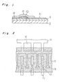
- Fig. 5 is a construction view of a conventional thick membrane type of thermal head.
- a glaze layer 2 is formed on the top face of the alumina base plate 1, a common electrode 3 and an individual electrode 4, a heating resistor 5 are formed on it, with an abrasion layer 6 being provided to cover the respective one portion of the heating resistor 5, the electrodes 3, 4.
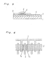
- Fig. 6 is a plan view showing an electrode shape of another conventional thick membrane type of thermal head.
- a a line-shaped common heating resistor 5 is provided, with the conductive electrodes for energization use 3, 4 having the common electrode 3 and the individual electrode 4 introduced, disposed, in a zigzag shape, alternately from both the sides of the heating resistor 5.
- one dot is constructed in one individual electrode 4, with two heating portions 7a, 7b being provided correspondingly. Namely, upon the application of voltage in pulse upon between one individual electrode 4 and a common electrode 3, a current flows at the same time to the heating portions 7a, 7b so as to form two color forming points.
- the resistor values of the heating member of the thick membrane type thermal head having the electrode shape of the zigzag type have the dispersion of ten-odd percent in a plurality of dots within the same head.
- the resistance value of the dot may be uniformly adjusted into approximately ⁇ 1 % through the trimming operation by the use of an energization overload trimming system (a method of using the resistance value variation through self-generating Joule heat to be caused when the power is fed into the heating resistor), but the calorific value per unit value of the heating resistor can not be made uniform.
- an essential object of the present invention is to provide a thermal head, which relates to an energization electrode shape of the thermal head, and is characterized in that the electrode shape is in construction of an approximately full periphery surrounding type of electrode un- precedentedly new, with an object of improving the heating efficiency in the printing to improve the thermal response property and to save the power. Namely, it is possible to correspond one heating portion with respect to one individual electrode without the separation and independence of the heating resistor.
- Another important object of the present invention is to provide a thermal head of the above-described type, which is characterized in that the approximately full periphery surrounding type of electrode portion is adapted to be completely covered by the heating resistor to remove the dispersion of the respective dot resistance values responsible for the dispersion of the printing width of the heating resistor, and to arrange it completely uniform by the energization overload trimming system.
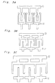
- a thermal head comprises a base plate, a common electrode on said base plate, said common electrode having a plurality of electrode end portions extending therefrom, a group of individual electrodes on said base plate, said individual electrodes extending between respective said electrode end portions of said common electrode, a heating resistor for energization by energization of said individual electrodes together with respective said electrode end portions, and electrode portions substantially surrounding the entire periphery of an end portion of said common electrode or the entire periphery of an individual electrode, and is characterized in that said electrode portions comprise swollen portions on two said end portions of said common electrode adjacent an individual electrode.
- the thermal head is characterized in that said electrode portions surround substantially the entire periphery of an individual electrode and comprise two end members extending from each said electrode end portion on either side of a respective individual electrode.
- the thermal head is characterized in that said electrode portions surround substantially the entire periphery of an individual electrode and comprise perpendicular portions extending substantially perpendicularly from an individual electrode at a position spaced from the end of an individual electrode.
- the thermal head is characterized in that said electrode portions form a part of an individual electrode and surround substantially the entire periphery of an electrode end portion.
- the invention provides a thermal head which is better in heating efficiency and thermal response property, is capable of high- qualtity printing by the improvements in toner recording property through the removal of uneven printing concentration of the respective dots, and is extremly reliable.
- a common electrode 10 and an individual electrode 11 made of a gold conductor are provided at an interval of dot pitch (16.7 /1.m) on the alumina base plate 8 with a glaze layer 9 provided thereon.
- the electrode construction at this time is one, wherein the power introduction portion of the common electrode 10 is disposed on approximately full periphery of the power introduction portion of the individual electrode 11 as shown in Fig. 2, namely, is an electrode construction of an approximately full periphery surrounding type.
- the heating resistor (4 through 8 /1.m in thickness) mainly made of Ru02 is print-burned in the line shape (350 /1.m in width), with the heating resistor 13 being formed on the opposite portion of the electrode group, then the glass layer is burned so as to cover one portion of the resistor and the electrode group, so that the abrasion-proof layer 12 (4 through 8 ⁇ m) in thickness is formed.
- the resistor values of the respective heating portions to be formed between the opposite common electrode 10 and the individual electrode 11 after the head formation are 1500 Q ⁇ 7 % although they are different in the electrode width of the opposite portion. It is to be noted that the end portion of the common electrode 10 is swollen into the common electrode swollen portion 14, with one portion of the individual electrode 11 being formed a narrow portion 15.
- the reference numeral 16 is a hollow portion disposed in one portion of the common electrode.
- the pulse voltage (5 through 150 V, several us) is energized for an optional time period onto the respective heating portion to be formed between the electrodes of a pair of opposite common electrode 10 and the individual electrode 11 so as to separately adjust the resistor values of the respective heating portions for the arrangement of the resistor values of all the heating portions within ⁇ 1 %.
- the conventional head with only the electrode pattern being supposed to be the conventional zigzag type of electrode pattern for comparison of the head is driven on the conditions of 0.4 W/Dot, 1/4 duty, 16 ms/cycle to print on the heat sensitive paper, according to the results of the concentration of the color forming point of the respective dot measured by a micro densitometer, the conventional head has the dispersion of ⁇ 5 % or more in the concentration of the color forming point, while the head of the present invention has the dispersion within ⁇ 2 %, thus allowing the extremely high quality of printing operation.
- the head with the construction of the end portion of the electrode of the electrode group for introducing the heating power into the heating member being in the construction of the electrode of approximately full periphery surrounding type is 1.2 time as high in the printing concentration as compared with the head of the conventional simple zigzag type of electrode pattern, and is superior in the thermal response property.
- the printing condition in the actual printing allows the extremely high quality of printing to be effected as compared with the conventional simple zigzag type of head, because the color formation of the first line is clear.
- the heating resistor (0.5 through 8 ⁇ m in thickness) including Ru02 on the alumina base plate with the glaze layer provided thereon is printed, burned in a line shape (400 ⁇ m in width) to form the heating resistor, then a common electrode and an individual electrode each being composed of a gold elect ⁇ rode (0.5 through 1.0 ⁇ m) is provided at an interval of the dot pitch (16.7 /1 .m).
- the electrode construction at this time is one, wherein the end portion of the common electrode was disposed on approximately full periphery of the end portion of the individual electrode as shown in Fig. 2, namely, the electrode construction of an approximately full periphery surrounding type.
- the glass layer is printed, burned so as to cover the one portion of the resistor and the electrode group to form the abrasion-proof layer (4 through 8 ⁇ m in thickness).
- the extremely high quality of printing is effected, with the dispersion within ⁇ 2 % in the printing concentration. Furthermore, it is found out that the printing concentration is 1.2 time as high as compared with the head of the conventional simple zigzag type of electrode pattern, with the head being superior in thermal response property. Also, from the printing condition in the actual printing operation, it is found out that the extremely high quality printing may be effected as compared with the conventional simple zigzag type of head, with the first line of color formation being clear.
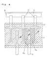
- Fig. 4 is a plan view for illustrating the thermal head in a different embodiment of the present invention.
- the electrodes 19a, 19b for energization use of the first group and the second group composed of the gold (0.5 through 1.0 ⁇ m) alternately introduced, disposed onto the alumina base plate 18 provided on the glaze layer are disposed at the interval of the dot pitch (167 /1 .m).
- the one conductor electrode 122 is connected with the individual electrode 20, and the conductor electrode 19 is connected with a common electrode 21.
- the electrode construction at this time is one, wherein the end portion of the first group of individual electrode 20 is disposed on the full periphery of the end portion of the electrode 19, the end portion for the common electrode use of the second group is disposed, namely, so as to provide the electrode construction of a full periphery surrounding type.
- the resistance material for heating use mainly composed Ru02 is printed, burned in a line shape (350 /1.m in width) on the opposite portion of the electrode group so as to form the heating resistor 22 (4 through 8 ⁇ m in thickness), then the glass layer is printed, burned so as to cover one portion of the resistor 22 and the electrode group to form the abrasion proof layer 23 (4 through 8 ⁇ m in thickness).
- the pulse voltages (5 through 200V, several us) is energized for an optional time separately into the respective heating portions, for example, 24a and 24b to be formed between the conductor 122 of the individual electrode 20 and a pair of adjacent conductor electrodes 19 for the common electrode 21 use so as to separately adjust the resistance value of the heating portion for arrangement of the resistance values of all the heating portions within ⁇ 1 %.
- the one portion of the electrodes of the second group is connected with the electrode group of the second group through printing, burning of the conductive material of a Cu - resin series as shown in a plan view showing the electrode shape of the thermal head in the drawing so as to form the common electrode 21.
- the resistance value of one dot is a composed value between the heating portions 24a and 24b to be formed between the end portions of a pair of electrodes 19 adjacent to the end portion of the individual electrode 20 as the second group of electrode groups is turned into the short condition by the common electrode 21.
- the composed resistance value of the heating portion is 1500 ⁇ 1 %.
- the conventional head with only the electrode pattern being the conventional zigzag type of electrode pattern for the comparison of the head is driven under the conditions of 0.4 W/dot, 1/4 duty, 16 ms/cycle to print on the heat sensitive paper, according to the results given about the concentration of the color forming point of the respective dot, the conventional head has the dispersion of ⁇ 10 % or more in the concentration of the color forming point, with the head of the present invention having the dispersion within ⁇ 1.5 %, with the printing being extremely high in quality.
- the head with the construction of the end portion of the electrodes of the electrode group to be introduced into the heating member being a full periphery surrounding electrode construction is 1.2 time as high in the printing concentration as compared with the head of the conventional simple zigzag type of electrode pattern, thus being superior in thermal response property.
- the first line color formation is clear and the extremely higher quality of printing may be effected as compared with the conventional simple zigzag head.
- the electrode shape is in the construction of the periphery surrounding type electrode with the common electrode end portion being provided on the periphery of the individual electrode end portion, the similar effected is obtained, and there is not, needless to say, any restriction to the embodiment.
- the thermal head may be an enamel one, and there is not, needless to say, any restriction even to the respective construction materials of the head.
- a resistor layer 1000 through 5000 ⁇
- Ta - Si is formed in a line shape (350 ⁇ m in width) on the electrode construction portion of the full periphery surrounding electrode by a vacuum thin membrane forming process
- an abrasion-proof layer 3 through 7 /1 .m
- SiC is formed to cover the resistor layer and the full periphery surrounding type electrode construction portion so as to manufacture the thin membrane type thermal head.
- the head of the present embodiment is found to be 1.1 time as high in the printing concentration as compared with the conventional thermal membrane type of thermal head and to be superior in thermal response property. Also, the similar effect is confirmed even in a case where the heating resistor and the electrode are formed upside down.
- the base plate of the thermal head may be an enamel base plate, and furthermore the particular limit is not given, needless to say, with respect to the respective construction materials of the head, the dot resistance value.
- the present invention relates to the electrode shape for energization use of the thermal head, and provides a thermal head, which is improved in the heating efficiency in the printing operation to increase the thermal response property and to save the power, and is improved in uneven printing concentration of the respective dots for better gradation recording property, is capable of high quality printing operation, is higher in reliability.
- the photolitho etching step of the resistor layer may be omitted even in the thin membrane type of thermal head, thus making it possible to have the lower cost.
Landscapes
- Electronic Switches (AREA)
Abstract
Claims (14)
caractérisée en ce que :
les parties d'électrode comprennent des parties élargies (14) formées sur deux parties d'extrémité de l'électrode commune (10 ; 21) près d'une électrode individuelle (11 ; 20).
les parties élargies (14) dépassent des extrémités des parties d'extrémité de l'électrode commune (10 ; 21) vers la partie rétrécie (15) d'une électrode individuelle (11 ; 20).
caractérisée en ce que :
les parties d'électrode entourent pratiquement toute la périphérie d'une électrode individuelle (11 ; 20) et comportent deux organes d'extrémité dépassant de chacune des parties d'extrémité d'électrode de part et d'autre d'une électrode individuelle respective (11 ; 20).
caractérisée en ce que :
les parties d'électrode entourent pratiquement toute la périphérie d'une électrode individuelle (11) et comportent des parties perpendiculaires qui sont sensiblement perpendiculaires à une électrode individuelle (11) à un emplacement distant de l'extrémité d'une électrode individuelle (11).
caractérisée en ce que :
les parties d'électrode font partie d'une électrode individuelle (11 ; 20) et entourent pratiquement toute la périphérie d'une partie d'extrémité d'électrode.
les parties d'électrode comportent en outre une partie élargie aux extrémités des organes d'extrémité de l'électrode individuelle, les parties élargies dépassant des organes d'extrémité vers la partie rétrécie de la partie d'extrémité d'électrode.
une couche (12 ; 23) résistant à l'abrasion est placée sur la résistance de chauffage (13 ; 22) et les parties d'extrémité d'électrode de l'électrode commune (10 ; 21) et des électrodes individuelles (11 ; 20).
Applications Claiming Priority (4)
| Application Number | Priority Date | Filing Date | Title |
|---|---|---|---|
| JP292327/87 | 1987-11-19 | ||
| JP62292327A JPH01133756A (ja) | 1987-11-19 | 1987-11-19 | サーマルヘッド |
| JP38951/88 | 1988-02-22 | ||
| JP63038951A JPH01214453A (ja) | 1988-02-22 | 1988-02-22 | サーマルヘッドおよびその製造法 |
Publications (3)
| Publication Number | Publication Date |
|---|---|
| EP0342243A1 EP0342243A1 (fr) | 1989-11-23 |
| EP0342243A4 EP0342243A4 (fr) | 1990-02-21 |
| EP0342243B1 true EP0342243B1 (fr) | 1993-07-28 |
Family
ID=26378261
Family Applications (1)
| Application Number | Title | Priority Date | Filing Date |
|---|---|---|---|
| EP88910095A Expired - Lifetime EP0342243B1 (fr) | 1987-11-19 | 1988-11-17 | Tete d'impression thermique |
Country Status (5)
| Country | Link |
|---|---|
| US (1) | US5003324A (fr) |
| EP (1) | EP0342243B1 (fr) |
| KR (1) | KR920004866B1 (fr) |
| DE (1) | DE3882698T2 (fr) |
| WO (1) | WO1989004767A1 (fr) |
Families Citing this family (8)
| Publication number | Priority date | Publication date | Assignee | Title |
|---|---|---|---|---|
| EP0454133A3 (en) * | 1990-04-26 | 1993-01-13 | Matsushita Electric Industrial Co., Ltd. | Thermal print head trimming apparatus and method for trimming resistance of a thermal print head |
| KR0147671B1 (ko) * | 1995-11-02 | 1998-08-17 | 김광호 | 감열 기록 소자 |
| DE69714381T2 (de) * | 1996-05-30 | 2003-03-20 | Rohm Co. Ltd., Kyoto | Kopfgerät mit treiber-ic's, auf die eine schutzbeschichtung aufgebracht ist, und verfahren zum bilden der schutzbeschichtung |
| GB2366764B (en) * | 1997-10-02 | 2002-05-01 | Asahi Optical Co Ltd | Thermal line head and ink transfer printer using same |
| CA2249234A1 (fr) | 1997-10-02 | 1999-04-02 | Asahi Kogaku Kogyo Kabushiki Kaisha | Tete d'impression thermique et imprimante a transfert d'encre utilisant celle-ci |
| JP3469461B2 (ja) * | 1998-05-08 | 2003-11-25 | ローム株式会社 | 厚膜型サーマルプリントヘッド |
| JP2007245667A (ja) * | 2006-03-17 | 2007-09-27 | Sony Corp | サーマルヘッド及びプリンタ装置 |
| WO2013121837A1 (fr) | 2012-02-13 | 2013-08-22 | 株式会社村田製作所 | Ventilateur piézoélectrique |
Family Cites Families (4)
| Publication number | Priority date | Publication date | Assignee | Title |
|---|---|---|---|---|
| JPS5968270A (ja) * | 1982-10-12 | 1984-04-18 | Nippon Kogaku Kk <Nikon> | サ−マルヘツド用発熱抵抗体の製造法 |
| JPS605842U (ja) * | 1983-06-13 | 1985-01-16 | ロ−ム株式会社 | サ−マルプリントヘツド |
| JPS605842A (ja) * | 1983-06-24 | 1985-01-12 | Tanaka Kikinzoku Kogyo Kk | 刷子用摺動接点材料 |
| JPH0647296B2 (ja) * | 1985-03-15 | 1994-06-22 | ロ−ム株式会社 | サ−マルプリントヘツド |
-
1988
- 1988-11-17 EP EP88910095A patent/EP0342243B1/fr not_active Expired - Lifetime
- 1988-11-17 WO PCT/JP1988/001160 patent/WO1989004767A1/fr not_active Ceased
- 1988-11-17 DE DE88910095T patent/DE3882698T2/de not_active Expired - Fee Related
- 1988-11-17 KR KR1019890701354A patent/KR920004866B1/ko not_active Expired
- 1988-11-17 US US07/391,611 patent/US5003324A/en not_active Expired - Lifetime
Also Published As
| Publication number | Publication date |
|---|---|
| DE3882698D1 (de) | 1993-09-02 |
| EP0342243A1 (fr) | 1989-11-23 |
| EP0342243A4 (fr) | 1990-02-21 |
| DE3882698T2 (de) | 1994-02-24 |
| KR920004866B1 (ko) | 1992-06-19 |
| US5003324A (en) | 1991-03-26 |
| KR890701372A (ko) | 1989-12-20 |
| WO1989004767A1 (fr) | 1989-06-01 |
Similar Documents
| Publication | Publication Date | Title |
|---|---|---|
| US5003324A (en) | Thermal head | |
| US7352381B2 (en) | Thermal print head | |
| EP0679515A2 (fr) | Tête d'enregistrement | |
| JPH01133756A (ja) | サーマルヘッド | |
| JPH07112740B2 (ja) | サーマルヘッド | |
| JP2828327B2 (ja) | 厚膜型サーマルヘッド | |
| JPH0532297Y2 (fr) | ||
| JPH0751362B2 (ja) | サーマルヘツド | |
| JP2534041Y2 (ja) | 厚膜型サーマルヘッド | |
| JP3592440B2 (ja) | サーマルプリントヘッド | |
| JPH0419155A (ja) | 厚膜型サーマルヘッド | |
| JP2533087B2 (ja) | サ−マルヘツド | |
| JP2613304B2 (ja) | 厚膜型サーマルヘッド | |
| JPH01214453A (ja) | サーマルヘッドおよびその製造法 | |
| JPH0712703B2 (ja) | サーマルヘッド | |
| JPH0248960A (ja) | サーマルヘッド | |
| JPS63149165A (ja) | 厚膜サ−マルヘツド | |
| JP2530743Y2 (ja) | 厚膜型サーマルヘッド | |
| JP2965339B2 (ja) | サーマルヘッドの製造方法 | |
| JP2554556B2 (ja) | サ−マルプリントヘッド | |
| JPS6032587B2 (ja) | 感熱記録ヘツド | |
| JPS5968270A (ja) | サ−マルヘツド用発熱抵抗体の製造法 | |
| JPH03234551A (ja) | サーマルヘッド | |
| JPH01232068A (ja) | サーマルヘッド | |
| JPH04232763A (ja) | サーマルヘッド |
Legal Events
| Date | Code | Title | Description |
|---|---|---|---|
| PUAI | Public reference made under article 153(3) epc to a published international application that has entered the european phase |
Free format text: ORIGINAL CODE: 0009012 |
|
| AK | Designated contracting states |
Kind code of ref document: A1 Designated state(s): DE FR GB |
|
| 17P | Request for examination filed |
Effective date: 19890715 |
|
| A4 | Supplementary search report drawn up and despatched |
Effective date: 19900221 |
|
| 17Q | First examination report despatched |
Effective date: 19920130 |
|
| GRAA | (expected) grant |
Free format text: ORIGINAL CODE: 0009210 |
|
| AK | Designated contracting states |
Kind code of ref document: B1 Designated state(s): DE FR GB |
|
| REF | Corresponds to: |
Ref document number: 3882698 Country of ref document: DE Date of ref document: 19930902 |
|
| ET | Fr: translation filed | ||
| PLBE | No opposition filed within time limit |
Free format text: ORIGINAL CODE: 0009261 |
|
| STAA | Information on the status of an ep patent application or granted ep patent |
Free format text: STATUS: NO OPPOSITION FILED WITHIN TIME LIMIT |
|
| 26N | No opposition filed | ||
| REG | Reference to a national code |
Ref country code: GB Ref legal event code: 746 Effective date: 19950928 |
|
| REG | Reference to a national code |
Ref country code: FR Ref legal event code: D6 |
|
| REG | Reference to a national code |
Ref country code: GB Ref legal event code: IF02 |
|
| PGFP | Annual fee paid to national office [announced via postgrant information from national office to epo] |
Ref country code: FR Payment date: 20041109 Year of fee payment: 17 |
|
| PGFP | Annual fee paid to national office [announced via postgrant information from national office to epo] |
Ref country code: DE Payment date: 20041111 Year of fee payment: 17 |
|
| PGFP | Annual fee paid to national office [announced via postgrant information from national office to epo] |
Ref country code: GB Payment date: 20041117 Year of fee payment: 17 |
|
| PG25 | Lapsed in a contracting state [announced via postgrant information from national office to epo] |
Ref country code: GB Free format text: LAPSE BECAUSE OF NON-PAYMENT OF DUE FEES Effective date: 20051117 |
|
| PG25 | Lapsed in a contracting state [announced via postgrant information from national office to epo] |
Ref country code: DE Free format text: LAPSE BECAUSE OF NON-PAYMENT OF DUE FEES Effective date: 20060601 |
|
| GBPC | Gb: european patent ceased through non-payment of renewal fee |
Effective date: 20051117 |
|
| PG25 | Lapsed in a contracting state [announced via postgrant information from national office to epo] |
Ref country code: FR Free format text: LAPSE BECAUSE OF NON-PAYMENT OF DUE FEES Effective date: 20060731 |
|
| REG | Reference to a national code |
Ref country code: FR Ref legal event code: ST Effective date: 20060731 |