EP0343838A2 - CMOS-Aufwärts/Abwärts-Zähler - Google Patents
CMOS-Aufwärts/Abwärts-Zähler Download PDFInfo
- Publication number
- EP0343838A2 EP0343838A2 EP89304970A EP89304970A EP0343838A2 EP 0343838 A2 EP0343838 A2 EP 0343838A2 EP 89304970 A EP89304970 A EP 89304970A EP 89304970 A EP89304970 A EP 89304970A EP 0343838 A2 EP0343838 A2 EP 0343838A2
- Authority
- EP
- European Patent Office
- Prior art keywords
- counter
- output
- binary
- signal
- recited
- Prior art date
- Legal status (The legal status is an assumption and is not a legal conclusion. Google has not performed a legal analysis and makes no representation as to the accuracy of the status listed.)
- Ceased
Links
Images


Classifications
-
- H—ELECTRICITY
- H03—ELECTRONIC CIRCUITRY
- H03K—PULSE TECHNIQUE
- H03K23/00—Pulse counters comprising counting chains; Frequency dividers comprising counting chains
- H03K23/40—Gating or clocking signals applied to all stages, i.e. synchronous counters
- H03K23/50—Gating or clocking signals applied to all stages, i.e. synchronous counters using bi-stable regenerative trigger circuits
- H03K23/56—Reversible counters
-
- H—ELECTRICITY
- H03—ELECTRONIC CIRCUITRY
- H03K—PULSE TECHNIQUE
- H03K23/00—Pulse counters comprising counting chains; Frequency dividers comprising counting chains
- H03K23/40—Gating or clocking signals applied to all stages, i.e. synchronous counters
- H03K23/50—Gating or clocking signals applied to all stages, i.e. synchronous counters using bi-stable regenerative trigger circuits
- H03K23/52—Gating or clocking signals applied to all stages, i.e. synchronous counters using bi-stable regenerative trigger circuits using field-effect transistors
-
- H—ELECTRICITY
- H03—ELECTRONIC CIRCUITRY
- H03K—PULSE TECHNIQUE
- H03K3/00—Circuits for generating electric pulses; Monostable, bistable or multistable circuits
- H03K3/02—Generators characterised by the type of circuit or by the means used for producing pulses
- H03K3/027—Generators characterised by the type of circuit or by the means used for producing pulses by the use of logic circuits, with internal or external positive feedback
- H03K3/037—Bistable circuits
-
- H—ELECTRICITY
- H03—ELECTRONIC CIRCUITRY
- H03K—PULSE TECHNIQUE
- H03K3/00—Circuits for generating electric pulses; Monostable, bistable or multistable circuits
- H03K3/02—Generators characterised by the type of circuit or by the means used for producing pulses
- H03K3/353—Generators characterised by the type of circuit or by the means used for producing pulses by the use, as active elements, of field-effect transistors with internal or external positive feedback
- H03K3/356—Bistable circuits
- H03K3/356017—Bistable circuits using additional transistors in the input circuit
- H03K3/356052—Bistable circuits using additional transistors in the input circuit using pass gates
- H03K3/35606—Bistable circuits using additional transistors in the input circuit using pass gates with synchronous operation
-
- H—ELECTRICITY
- H03—ELECTRONIC CIRCUITRY
- H03K—PULSE TECHNIQUE
- H03K3/00—Circuits for generating electric pulses; Monostable, bistable or multistable circuits
- H03K3/02—Generators characterised by the type of circuit or by the means used for producing pulses
- H03K3/353—Generators characterised by the type of circuit or by the means used for producing pulses by the use, as active elements, of field-effect transistors with internal or external positive feedback
- H03K3/356—Bistable circuits
- H03K3/356069—Bistable circuits using additional transistors in the feedback circuit
- H03K3/356078—Bistable circuits using additional transistors in the feedback circuit with synchronous operation
Definitions
- This invention relates to binary counters and more particularly to a high speed binary up/down (U/D) counter implemented with CMOS technology having a plurality of multi-bit stages which may be concatenated in multiple sections.
- U/D binary up/down
- Binary ripple time counters are well known in the prior art. They have been implemented utilizing CMOS technologies but have the disadvantage of the carry rippling through each stage of the binary counter which takes a considerable amount of time. In order to decrease this carry ripple time, look-ahead circuits comprising AND or NAND gates have been used; however, such gates have required a significant amount of die area as the number of counter stages increases thereby increasing the number of inputs to look-ahead gates. In addition, the time delays associated with the increased gating reduces the counting rate of such a binary counter.
- CMOS transmission gate look-ahead carry circuit has been utilized in a CMOS synchronous binary counter as described in U.S. Patent No. 3,943,378, inventor R. R. Beutler, which requires only a small amount of die area.
- this is a counter with ripple carry employing a carry pass structure which looks at the previous stage employing toggle flip-flops to effect a count; a compromise is made between obtaining a higher speed binary counter and minimizing usage of the die area.
- a CMOS binary up/down counter is described in U.S. Patent No. 4,611,337 to Michael W. Evans.
- a counter stage comprises an exclusive-OR gate, a D-type flip-flop and a multiplexer interconnected to operate in accordance with a clock signal and a U/D control signal.
- the fabrication of a multiplexer in CMOS technology is simpler than such implementation in bipolar transistor-transistor-logic (TTL) technology.
- TTL bipolar transistor-transistor-logic
- each stage requires a multi-input AND gate having the number of inputs equal to its stage position in the counter, with the last stage having an N input AND gate; this results in the inefficient use of die area of a CMOS integrated circuit.
- CMOS binary counters An improvement in the art of high speed CMOS binary counters is described in U.S. Patent Application Serial No. 033,381 entitled CMOS Binary Counter filed by Edward T. Lewis and assigned to the present assignee.
- each 4-bit counter section performs a counting function through a successive process of additions of a lowest order stage carry input, and each bit stage within a 4-bit section uses the current state of each stage to determine what happens in the next stage.
- a carry-forward generator instead of a carry-generation network provides a carry-forward signal to the next 4-bit counter section with a worse case delay of only a 2-input gate delay thereby enabling high speed operation.
- a high speed CMOS binary up/down counter is provided without the need for cumbersome carry signal gating structures comprising a 4-bit up/down counting section that may be concatenated in multiple 4-bit sections.
- Each bit stage of a 4-bit section comprises means for storing a bit of a binary count, the storing means having a data input, a clock input, a first output providing the bit of the binary count and a second output providing a complement signal of the first output, means having an output coupled to the input of the storing means for performing a modulo-two sum of a lower order carry signal and the first output or the second output of the storing means in accordance with an up/down mode selection signal, and means coupled to the up/down mode selection signal and the lower order carry signal for determining whether to propagate/kill or propagate/generate a higher order carry signal in accordance with the state of the up/down mode selection signal and the first output or second output of the storing means in accordance with the state of the up/down mode selection
- the up/down counter comprises a selector means coupled to the first output and the second output of the storing means for selecting whether the first output or the second output of the storing means is coupled to the modulo-two summing means and the higher order carry determining means in accordance with the state of the up/down mode selection signal. Since there is no lower order carry signal for a first stage of the counter, an equivalent signal is generated by a count selector means in accordance with the state of the up/down mode selection signal.
- the counter operates an up-counter when the up/down mode selection signal is a logic one and the counter operates as a down-counter when the mode selection signal is a logic zero.
- Each section of the up/down binary counter comprises carry-forward generation means coupled to the outputs of each stage of a section, an output from a previous adjacent carry-forward generating means and a first bit output of a first one of the sections of the counter for generating a carry-forward signal.
- Each storing means in each counter stage comprises a reset input for resetting the counter to zero.
- a method of performing binary up/down counting with a plurality of sequentially coupled stages comprising the steps of storing a bit of a binary count in a storing means having a data input, a clock input, a first output providing the bit of the binary count and a second output providing a complement signal of the said first output, performing a modulo-two sum of a lower order carry signal and the first output or the second output of the storing means in accordance with an up/down mode selection signal, the result of the modulo-two sum being coupled to said input of said storing means, and determining whether to propagate/kill or propagate/generate a higher order carry signal in accordance with the state of the up/down mode selection signal and the first output or the second output of the storing means in accordance with the state of the up/down mode selection signal.
- the method comprises the step of generating the lower order carry signal for a first stage of the counter by a count selector means in accordance with the state of the up/down mode selection signal.
- the method comprises the step of operating as an up-counter when the up/down mode selection signal is a logic one and of operating as a down-counter when the up/down mode selection signal is a logic zero.
- the method further comprises the step of resetting said binary count in said storing means to zero.
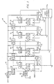
- Fig. 1 there is shown a functional block diagram of a 4-bit section 10 of a complementary metal oxide semiconductor (CMOS) high speed binary up/down counter having four sequentially coupled stages capable of operating at greater than a 200 MHZ clock rate.
- the 4-bit section 10 performs either an increment (up-count) or a decrement (down-count) in accordance with an up/down count mode select signal.
- CMOS complementary metal oxide semiconductor
- each stage 11 of the four stages within section 10 comprises a D-type flip-flop 12, 14, 16, 18 for count storage and a modulo-two (M-2) summer 20, 22, 24, 26 for performing two's complement addition, each output of said modulo-two summer S0, S1, S2, S3 being coupled to an input of each D-type flip-flop 12, 14, 16, 18 respectively.
- M-2 modulo-two
- each output of said modulo-two summer S0, S1, S2, S3 being coupled to an input of each D-type flip-flop 12, 14, 16, 18 respectively.
- P/K/G propagate/kill/generate
- the P/K/G gate 20-26 function is to propagate a carry, kill a carry or generate a carry.
- the fourth stage of section 10 does not have a P/K/G gate because of a carry-forward generator 34 logic network having inputs coupled to the outputs of each of the 4 stages in counter section 10.
- the carry-forward generator 34 provides a carry-forward signal (CF i ) to another 4-bit counter section when counter sections are concatenated as shown in Fig. 4.
- Each P/K/G gate 28-32 has an input coupled to an output of a 2:1 selector 40, 42, 44, 46 respectively.
- the Q and Q outputs of each D-type flip-flop 12-18 are coupled to the inputs of the 2:1 selector 40-44 respectively.
- each P/K/G gate 28-32 has an input coupled to an output of a previous P/K/G gate except the first stage 11 of the counter section 10 that receives a signal from a count selector 38 which is a logic one for an up-count and a logic zero for a down-count.
- the count selector 38 output signal is also coupled to an input of M-2 summer 20.
- the input to the count selector 38 is an up/down mode control select signal (U/D) which is also coupled to the 2:1 selector 40-46 and the P/K/G gate 28-32 of each counter stage.
- the up/down counting sequence is determined by the U/D level signal input.
- Fig. 1 and Table 1 the status of signals in counter section 10 is shown when performing an up-count from decimal 0 to 10.
- First the U/D signal is set to a logic one level to perform an up-count which puts the count selector 38 in the logic one state.
- the count selector 38 is only present in the lowest order bit position and is used to establish the initial carry input state.
- the 2:1 selector 40 is set by the U/D signal to sample the Q-state of the D-type flip-flop 12.
- the P/K/G gate 28 is also set by the U/D signal to sample the present state of the Q output and perform only a P/K function of the P/K/G/ gate 28 to either propagate a carry or to kill a carry because the G path is disabled as a result of being in the up-count mode. Assume that the up-count is starting from an all zero count wherein all the D-flip-flops 40-46 are reset to a logic zero. Before the count enable (CE) is raised to the logic one state, the output of each counter stage A1, A2,...A i is sampled.
- the P/K/G gate samples the state of A0 and performs a kill (K) operation (generate a logic 0 at P/K/G gate output, C0), if A0 is in the logic zero state, or it performs a propagate (P) operation if A0 is in the logic one state. However, in this case A0 equals zero and the P/K/G gate 28 is placed in the K state and essentially becomes the "CS like" signal to the next stage.
- the states of S0 and S1 are transferred to the A0 and A1 counter outputs respectively. In this case A0 goes to zero and A1 goes to one, and the binary number (0010)2 is stored in counter section 10. Additional clock signals result in the signal states shown in Table 1 when ten clock pulses have occurred.
- Table 2 shows the status of signals in counter section 10 when down-counting, arbitrarily starting at the 4-bit binary number (0110)2.
- the down-count mode is established by setting the U/D signal level to a logic zero state which causes the 2:1 selectors 40-46 to select the Q outputs of the D-type flip-flops in the counter section 10, sets the count select 38 output signal to a logic zero state, and selects the P/G function of the P/K/G gates 28-32.
- the decrementing operation is performed through the process of two's complement addition similar to that for up-counting.
- the logic operations are summarized in Table 2.
- the down-counting and up-counting modes of operation are enabled by only the U/D signal. This signal may be changed when the clock (CLK) is in the logic zero state.
- the counter outputs (A0, A1,....A i ) retain the last count.
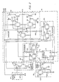
- FIG. 2 a more detailed diagram of the first stage 11 of the 4-bit binary up/down counter section 10 is shown along with the circuits for the count enable gate 36, buffer 37 and count selector 38.
- the storage element of each counter stage 11 is implemented with a D-type flip-flop 12 having its CLK input connected to the count pulse (CP) output signal of the count enable gate 36.
- the D in input of the D-type flip-flop 12 is connected to the S0 output of the modulo-two summer 20.
- the reset signal to the R input of the D-type flip-flop is a general reset line for resetting the counter TABLE 2 DOWN-COUNT OPERATION U/D CS CLOCK COUNT (DECIMAL) A0 A1 A2 A3 CO P/G)0 C1 P/G)1 C2 P/G)2 S0 S1 S2 S3 0 0 0 0 1 1 0 0 1 1 1 0 1 0 0 0 1 1 0 1 0 1 0 1 0 0 1 0 0 0 0 2 0 0 1 0 0 0 0 0 1 1 1 0 0 0 0 0 3 1 1 0 0 1 1 1 0 1 0 0 0 0 4 0 1 0 0 0 0 1 1 1 0 0 0 0 0 5 1 0 0 0 0 1 1 1 0 0 0 0 0 6 0 0 0 0 0 0 0
- Q and Q output signals of D-type flip-flop 12 are connected to transmission gates (T-gates) 100 and 102 respectively of a 2:1 selector 40.
- T-gates transmission gates
- the 2:1 selector 40 selects the Q output
- the 2.l selector 40 selects the Q output.
- the output of the 2:1 selector 40 is coupled to a P/K/G gate 28. This output goes through inverters 106 and 108 to obtain the required logic levels.
- the output from inverter 106 is coupled also to M-2 summer 20.
- the P/K/G gate 28 comprises a propagate T-gate 110, a generate T-gate 114 and a kill T-gate 118.
- the U/D signal determines which portions of the P/K/G gate functions during an up-count mode and during a down-count mode. For example, in the up-count mode (U/D equals logic one and U/D equals logic zero) the 2:1 selector samples the Q output of D-type flip-flop 12 and the P/K/G gate 28 is set up in a P/K mode to either propagate a carry, Ci, or kill such a carry.
- T-gate 110 passes the carry signal, Ci, in accordance with its input from the count selector 38 or a previous P/K/G gate (for other stages), or T-gate 118 kills or prevents passage of a carry signal, Ci, by causing transistor 126 to be in a conducting or ON state.
- the 2:1 selector samples the Q output of D-type flip-flop 12 and the P/K/G gate 28 is set up in a P/G mode to either propagate a carry, Ci, or generate such a carry.
- T-gate 110 passes a carry in accordance with its input from the count selector 38 or a previous P/K/G gate (for other stages), or T-gate 114 generates a carry by causing transistor 124 to be in a conducting or ON state.
- the M-2 Summer 20 comprises T-gates 134 and 138 arranged to perform an exclusive-OR logic function.
- Inverters 130 and 132 generate the appropriate polarity signals for performing the exclusive-OR function on two signal inputs, a first input signal being a CS signal from the count selector 38 when the M-2 summer 20 is in the first stage of the counter section 10 (or in subsequent stages the first input signal being a Ci signal from a previous P/K/G gate output) and a second in-put signal being the output from the 2:1 selector 40.
- the M-2 summer essentially generates partial sums during the operation of the counter section 10 and the partial sum output S0 is coupled to the D in input of D-type flip-flop 12.
- the count enable gate 36 comprises an AND T-gate for generating a count pulse (CP) when the CLK and CE signals are both asserted so the counting occurs synchronous with the clock.
- the inverter 152 provides the appropriate CP logic level.
- the buffer 37 comprises two inverters 140 and 142 for providing the required signal gain and both the U/D logic one signal and the U/D logic zero signal for use within a counter section 10.
- the count selector 38 comprises transistors 144 and 146 which act as switches for generating the CS signal as a logic one or a logic zero depending on whether the counter is in the up-count mode or the down-count mode respectively.
- CMOS D-type flip-flop 12-18 comprising CMOS transmission gates 73, 75, 87, and 91 for implementation in a binary counter section 10.
- AND gate 78 provides for a synchronous reset capability.
- An inverter 82 functions as a clock buffer/driver for use by the CLK signal within each flip-flop 12-18 of a counter section 10.
- Inverter 94 and 96 are enhanced to provide an intermediate drive capability for the Q and Q output signals of the D-type flip-flop.
- the use of a D-type flip-flop instead of, for example, a toggle flip-flop, provides for data to already be stored and ready for a clock signal thereby eliminating any delay time consideration of the flip-flop itself from reducing the counter speed.
- FIG. 4 three binary counter sections 101, 102, 103 are shown in a concatenated embodiment resulting in a 12 stage binary up/down counter with outputs A0-A11.
- the U/D mode control signal is provided for selecting whether the binary counter functions as an up-counter or a down-counter.
- the CLK signal is provided to each counter section 101, 102, 103 along with the CE signal to each counter section. Within each section the actual process of counting commences when the count enable (CE) signal is raised to a logic one state while the input clock (CLK) signal is in the logic zero state.
- CE count enable
- CLK input clock
Landscapes
- Error Detection And Correction (AREA)
- Logic Circuits (AREA)
- Complex Calculations (AREA)
Applications Claiming Priority (2)
| Application Number | Priority Date | Filing Date | Title |
|---|---|---|---|
| US199831 | 1988-05-26 | ||
| US07/199,831 US4856035A (en) | 1988-05-26 | 1988-05-26 | CMOS binary up/down counter |
Publications (2)
| Publication Number | Publication Date |
|---|---|
| EP0343838A2 true EP0343838A2 (de) | 1989-11-29 |
| EP0343838A3 EP0343838A3 (de) | 1990-10-31 |
Family
ID=22739204
Family Applications (1)
| Application Number | Title | Priority Date | Filing Date |
|---|---|---|---|
| EP19890304970 Ceased EP0343838A3 (de) | 1988-05-26 | 1989-05-17 | CMOS-Aufwärts/Abwärts-Zähler |
Country Status (3)
| Country | Link |
|---|---|
| US (1) | US4856035A (de) |
| EP (1) | EP0343838A3 (de) |
| JP (1) | JP2563578B2 (de) |
Cited By (1)
| Publication number | Priority date | Publication date | Assignee | Title |
|---|---|---|---|---|
| EP0746108A3 (de) * | 1995-05-24 | 1998-02-11 | HE HOLDINGS, INC. dba HUGHES ELECTRONICS | Schaltung für schnellen Synchronzähler |
Families Citing this family (24)
| Publication number | Priority date | Publication date | Assignee | Title |
|---|---|---|---|---|
| GB2273835B (en) * | 1992-12-22 | 1996-08-14 | Advanced Risc Mach Ltd | Bistable circuit |
| KR950015184B1 (ko) * | 1993-11-08 | 1995-12-23 | 삼성전자주식회사 | 동기식 이진카운터 |
| ES2078173B1 (es) * | 1993-12-30 | 1998-01-16 | Alcatel Standard Electrica | Arquitectura de circuitos integrados digitales. |
| KR0135488B1 (ko) * | 1994-05-26 | 1998-06-15 | 김광호 | 동기카운터 및 그 캐리전파방법 |
| US6449329B1 (en) * | 2000-09-14 | 2002-09-10 | Qualcomm Incorporated | Dual-edge M/N:D counter |
| US6826249B1 (en) * | 2002-10-10 | 2004-11-30 | Xilinx, Inc. | High-speed synchronous counters with reduced logic complexity |
| KR100834763B1 (ko) * | 2006-11-14 | 2008-06-05 | 삼성전자주식회사 | 동적 촬영 대역의 확장을 위한 이미지 센서 및 화소에수광된 광량을 측정하는 방법 |
| US8045662B2 (en) * | 2007-06-22 | 2011-10-25 | Texas Instruments Incorporated | Binary ripple counter sampling with adjustable delays |
| US9692429B1 (en) * | 2012-11-15 | 2017-06-27 | Gsi Technology, Inc. | Systems and methods involving fast-acquisition lock features associated with phase locked loop circuitry |
| US9548135B2 (en) * | 2013-03-11 | 2017-01-17 | Macronix International Co., Ltd. | Method and apparatus for determining status element total with sequentially coupled counting status circuits |
| US10770133B1 (en) | 2016-12-06 | 2020-09-08 | Gsi Technology, Inc. | Read and write data processing circuits and methods associated with computational memory cells that provides write inhibits and read bit line pre-charge inhibits |
| US10998040B2 (en) | 2016-12-06 | 2021-05-04 | Gsi Technology, Inc. | Computational memory cell and processing array device using the memory cells for XOR and XNOR computations |
| US10725777B2 (en) | 2016-12-06 | 2020-07-28 | Gsi Technology, Inc. | Computational memory cell and processing array device using memory cells |
| US11227653B1 (en) | 2016-12-06 | 2022-01-18 | Gsi Technology, Inc. | Storage array circuits and methods for computational memory cells |
| US10943648B1 (en) | 2016-12-06 | 2021-03-09 | Gsi Technology, Inc. | Ultra low VDD memory cell with ratioless write port |
| US10777262B1 (en) | 2016-12-06 | 2020-09-15 | Gsi Technology, Inc. | Read data processing circuits and methods associated memory cells |
| US10847212B1 (en) | 2016-12-06 | 2020-11-24 | Gsi Technology, Inc. | Read and write data processing circuits and methods associated with computational memory cells using two read multiplexers |
| US10847213B1 (en) | 2016-12-06 | 2020-11-24 | Gsi Technology, Inc. | Write data processing circuits and methods associated with computational memory cells |
| US10860320B1 (en) | 2016-12-06 | 2020-12-08 | Gsi Technology, Inc. | Orthogonal data transposition system and method during data transfers to/from a processing array |
| US10854284B1 (en) | 2016-12-06 | 2020-12-01 | Gsi Technology, Inc. | Computational memory cell and processing array device with ratioless write port |
| US10891076B1 (en) | 2016-12-06 | 2021-01-12 | Gsi Technology, Inc. | Results processing circuits and methods associated with computational memory cells |
| US10877731B1 (en) | 2019-06-18 | 2020-12-29 | Gsi Technology, Inc. | Processing array device that performs one cycle full adder operation and bit line read/write logic features |
| US10930341B1 (en) | 2019-06-18 | 2021-02-23 | Gsi Technology, Inc. | Processing array device that performs one cycle full adder operation and bit line read/write logic features |
| US10958272B2 (en) | 2019-06-18 | 2021-03-23 | Gsi Technology, Inc. | Computational memory cell and processing array device using complementary exclusive or memory cells |
Family Cites Families (10)
| Publication number | Priority date | Publication date | Assignee | Title |
|---|---|---|---|---|
| SE323715B (de) * | 1964-05-21 | 1970-05-11 | Philips Svenska Ab | |
| US3798554A (en) * | 1971-12-29 | 1974-03-19 | Z Sadlak | Digital sequential circuit |
| US3870962A (en) * | 1973-04-25 | 1975-03-11 | Solitron Devices | Means to control pulse width and repetition rate of binary counter means |
| US3943378A (en) * | 1974-08-01 | 1976-03-09 | Motorola, Inc. | CMOS synchronous binary counter |
| JPS5227348A (en) * | 1975-08-27 | 1977-03-01 | Hitachi Ltd | Counter |
| US4214173A (en) * | 1978-03-03 | 1980-07-22 | Standard Microsystems Corp. | Synchronous binary counter utilizing a pipeline toggle signal propagation technique |
| DE2833211C2 (de) * | 1978-07-28 | 1982-06-09 | Siemens AG, 1000 Berlin und 8000 München | Asynchroner binärer Vorwärts-Rückwärtszähler |
| US4611337A (en) * | 1983-08-29 | 1986-09-09 | General Electric Company | Minimal logic synchronous up/down counter implementations for CMOS |
| US4741006A (en) * | 1984-07-12 | 1988-04-26 | Kabushiki Kaisha Toshiba | Up/down counter device with reduced number of discrete circuit elements |
| US4759043A (en) * | 1987-04-02 | 1988-07-19 | Raytheon Company | CMOS binary counter |
-
1988
- 1988-05-26 US US07/199,831 patent/US4856035A/en not_active Expired - Fee Related
-
1989
- 1989-05-17 EP EP19890304970 patent/EP0343838A3/de not_active Ceased
- 1989-05-26 JP JP1134458A patent/JP2563578B2/ja not_active Expired - Lifetime
Cited By (1)
| Publication number | Priority date | Publication date | Assignee | Title |
|---|---|---|---|---|
| EP0746108A3 (de) * | 1995-05-24 | 1998-02-11 | HE HOLDINGS, INC. dba HUGHES ELECTRONICS | Schaltung für schnellen Synchronzähler |
Also Published As
| Publication number | Publication date |
|---|---|
| EP0343838A3 (de) | 1990-10-31 |
| JP2563578B2 (ja) | 1996-12-11 |
| US4856035A (en) | 1989-08-08 |
| JPH0229125A (ja) | 1990-01-31 |
Similar Documents
| Publication | Publication Date | Title |
|---|---|---|
| EP0343838A2 (de) | CMOS-Aufwärts/Abwärts-Zähler | |
| US6356112B1 (en) | Exclusive or/nor circuit | |
| US5060243A (en) | Ripple counter with reverse-propagated zero detection | |
| US4002926A (en) | High speed divide-by-N circuit | |
| US4759043A (en) | CMOS binary counter | |
| US4780894A (en) | N-bit gray code counter | |
| Mahmoud et al. | A 10-transistor low-power high-speed full adder cell | |
| US4433372A (en) | Integrated logic MOS counter circuit | |
| US4741004A (en) | High-speed programmable divide-by-N counter | |
| EP0097779B1 (de) | Logikschaltung | |
| JP3198379B2 (ja) | 最大値選択回路 | |
| US3818242A (en) | High-speed logic circuits | |
| US4937845A (en) | Fast library element gray code generators without feedback and feedforward networks | |
| EP0238091A2 (de) | Logikschaltung | |
| CN108777575B (zh) | 分频器 | |
| EP0281094B1 (de) | Zähler | |
| US4360742A (en) | Synchronous binary-counter and programmable rate divider circuit | |
| EP0365224A2 (de) | I.C.-Zählerschaltung mit sich nicht überlappendem zweiphasigem Taktsignal | |
| JPS61252715A (ja) | Mビツト2進カウンタ | |
| JP2804421B2 (ja) | 係数切替プリスケーラ | |
| JPS648857B2 (de) | ||
| RU213104U1 (ru) | Компаратор двоичных чисел в последовательном коде | |
| CN118573179B (zh) | 一种可逆加减计数电路及其切换方法 | |
| US5237597A (en) | Binary counter compiler with balanced carry propagation | |
| JP3696004B2 (ja) | 半導体回路 |
Legal Events
| Date | Code | Title | Description |
|---|---|---|---|
| PUAI | Public reference made under article 153(3) epc to a published international application that has entered the european phase |
Free format text: ORIGINAL CODE: 0009012 |
|
| AK | Designated contracting states |
Kind code of ref document: A2 Designated state(s): DE GB NL |
|
| PUAL | Search report despatched |
Free format text: ORIGINAL CODE: 0009013 |
|
| AK | Designated contracting states |
Kind code of ref document: A3 Designated state(s): DE GB NL |
|
| 17P | Request for examination filed |
Effective date: 19901211 |
|
| 17Q | First examination report despatched |
Effective date: 19920728 |
|
| STAA | Information on the status of an ep patent application or granted ep patent |
Free format text: STATUS: THE APPLICATION HAS BEEN REFUSED |
|
| 18R | Application refused |
Effective date: 19930723 |