EP0344475B1 - Tablette pour l'entrée de données - Google Patents
Tablette pour l'entrée de données Download PDFInfo
- Publication number
- EP0344475B1 EP0344475B1 EP89107864A EP89107864A EP0344475B1 EP 0344475 B1 EP0344475 B1 EP 0344475B1 EP 89107864 A EP89107864 A EP 89107864A EP 89107864 A EP89107864 A EP 89107864A EP 0344475 B1 EP0344475 B1 EP 0344475B1
- Authority
- EP
- European Patent Office
- Prior art keywords
- data input
- input tablet
- screen
- tablet according
- coated
- Prior art date
- Legal status (The legal status is an assumption and is not a legal conclusion. Google has not performed a legal analysis and makes no representation as to the accuracy of the status listed.)
- Expired - Lifetime
Links
Images
Classifications
-
- G—PHYSICS
- G06—COMPUTING OR CALCULATING; COUNTING
- G06F—ELECTRIC DIGITAL DATA PROCESSING
- G06F3/00—Input arrangements for transferring data to be processed into a form capable of being handled by the computer; Output arrangements for transferring data from processing unit to output unit, e.g. interface arrangements
- G06F3/01—Input arrangements or combined input and output arrangements for interaction between user and computer
- G06F3/03—Arrangements for converting the position or the displacement of a member into a coded form
- G06F3/041—Digitisers, e.g. for touch screens or touch pads, characterised by the transducing means
- G06F3/045—Digitisers, e.g. for touch screens or touch pads, characterised by the transducing means using resistive elements, e.g. a single continuous surface or two parallel surfaces put in contact
Definitions
- the invention relates to a data entry tablet according to the preamble of claim 1.
- a corresponding data entry tablet is known from US-A-4 207 444.
- Two electrically conductive levels face each other at a manageable distance.
- one level which serves to actuate the tray, is represented by a screen fabric.
- the electrical conductivity of the screen fabric is provided by the conductivity of its fabric thread.
- the inner surfaces of the mesh of the screen fabric are not electrically conductive. A line on the operating surface can therefore only be rasterized, i.e. can be reproduced in the grid of the screen fabric.
- JP 60-150124 A describes such a data input tablet with transparent surface electrodes.
- the space created by the frame between the surface electrodes is sealed and filled with an insulating, viscous mass.
- a data input tablet is known from EP 0 194 861 A2, with a conductive grid between the conductive surfaces which are kept at a distance by a frame.
- Such input trays are used to determine the coordinates of a writing tip which acts on the input surface of the tablet with writing pressure, e.g. of a stylus, to be recorded and made available for further electronic processing, such as display on a screen (DE 36 02 061 A1).
- writing pressure e.g. of a stylus
- display on a screen DE 36 02 061 A1
- spacers which can be punctiform or line-shaped, for example, and are distributed within the input surface. Surface parts of the input surface that can be directly assigned to such spacers are omitted for coordinate detection.
- the object is achieved by the feature of claim 1.
- the writing surface of which is cantilevered With such a data input tablet, the writing surface of which is cantilevered, the lines of the writing tip can be continuously detected; Electronic tracking circuits for bridging detection gaps on the spacers can be omitted.
- the electrical design of the data entry tablet can be designed according to the requirements of the data acquisition electronics. If necessary, e.g. the opposing surfaces of the rigid and the elastically deformable plane are coated in the same way homogeneously or in a pattern with a resistance film (DE-A-36 02 061). It is also conceivable to have a sheet resistance connected on all sides via point electrodes on the surface of the rigid plane, which is opposed by a surface with high conductivity which serves as a busbar under the action of a writing tip. Such a busbar can replace a system-specific, electrically functional stylus (EP-B-0 112 975).
- Screen fabrics made of metal-coated polymer fibers are tension-stable and relatively insensitive to sharp-edged objects.
- Fabrics made of nickel-coated polyester fibers have proven particularly useful for use in the input tray.
- the surface distance between the levels is determined exclusively by a frame-shaped spacer. The distance can be determined in the design phase of the data entry tablet, whereby it should be noted that 0.2 mm distance requires less writing pressure, whereas 0.6 mm distance makes the arrangement less sensitive for flat objects, e.g. for a lying hand .
- the main coating the inner surface of the sieve compensates for the fabric structure of the sieve, and carbon conductive varnishes also stabilize the contact resistance.
- An insulating layer smoothes the writing surface and thus refines the feeling of writing.
- Thermoplastic as a binder or as an insulating agent embrittles only to a small extent, it supports the elasticity of the screen surface.
- the substrate eg made of aluminum
- the substrate should be dimensioned such that the sieve tensioning forces ultimately acting on the substrate do not bend the same .
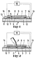
- the guide surface (4) of the elastically deformable plane (5) is arranged opposite the resistance layer (3).
- the elastically deformable plane is a sieve (6), which is carried under tension by a frame (7), so that the sieve (6) or its conductive layer (4) as the guide surface (4) of the elastically deformable plane (5) the resistance layer (3) is cantilevered at a distance (A).
- the screen (6) deforms under the pressure of a writing tip (8) (FIG. 2) and its conductive layer (4) makes contact with the resistance layer (3) in a contact point (9) after the distance (A) has been overcome.
- An evaluation circuit (10) detects the coordinates of the contact point (9) on the resistance layer and forms corresponding electrical signals for further processing.
- the substrate (1) of the embodiment is coated on both sides with a hot glue (11); on both sides in order to avoid bending stress on the substrate due to the coating.
- a resistance circuit with a very smooth surface is laminated into the hot-melt layer (11) on one side of the substrate (1).
- the resistance circuit comprises the resistance layer (3), which forms the electrically conductive surface of the rigid plane (2) with its surface, it further comprises the connection electrodes (12) of the resistance layer (3) and connection conductor tracks (13).
- the connection electrodes (12) which contact the resistance layer (3) on all sides as point electrodes are connected to the connection conductor tracks (13) via blocking diodes (14).
- the resistance circuit corresponds to the designs of EP-B-0 112 975.
- the screen fabric (6) is coated on one side with a thermoplastic conductive lacquer (4) with high conductivity; the surface of the conductive lacquer layer (4) forms the electrically conductive surface of the elastically deformable plane (5), which, across the data input tablet, opposes the resistance layer (3) spanning it.
- the conductive varnish is applied to the fine-mesh fabric using screen printing.
- a thermoplastic insulating film (15) is laminated on the second side of the screen fabric (6) provided as the outside.
- the screen fabric (6) is coated and the coatings (4, 15) are dried with the screen fabric held in a tensioning device. Such tensioners are common in screen printing technology.
- a frame (7) covered with epoxy adhesive on both sides is placed on the coated and still tensioned screen fabric on the side of the screen (6) coated with conductive lacquer (4).
- the tenter frame (7) is made of an electrically insulating material, for example hard paper, with a thickness of, for example, 0.5 mm.
- the previously finished substrate (1) is placed on the frame (7) in alignment with the resistance layer. After under the influence of pressure and heat, the substrate (1) with the frame (7) and the frame (7) with the Sieve cloth (6) are permanently connected, the frame (7) forms the distance (A). Removed or cut free from the tensioning device, the screen fabric (6) remains tensioned over the frame (7) stiffened on the substrate (1).
Landscapes
- Engineering & Computer Science (AREA)
- General Engineering & Computer Science (AREA)
- Theoretical Computer Science (AREA)
- Human Computer Interaction (AREA)
- Physics & Mathematics (AREA)
- General Physics & Mathematics (AREA)
- Position Input By Displaying (AREA)
- Mechanical Pencils And Projecting And Retracting Systems Therefor, And Multi-System Writing Instruments (AREA)
Claims (8)
- Plaquette d'entrée de données, destinée à relever par voie électrique les coordonnées d'une pointe marqueuse (8) et comportant un plan rigide (4) et un plan (5) déformable élastiquement, dont les faces conductrices (3, 4) se font vis-à-vis, sont maintenues isolées électriquement, à une distance (A) faible, l'une de l'autre, par un cadre (7) et qui, sous l'action de la pointe marqueuse (8), viennent en contact ponctuel sur la face extérieure du plan déformable (5), ce dernier étant un écran tissé (6), du genre d'un écran de sérigraphie, qui est, comme en sérigraphie, maintenu tendu par le cadre (7), plaquette caractérisée en ce que la face électriquement conductrice de l'écran est formée d'une couche conductrice compacte, déposée sur l'écran et composée d'un liant polymère dans lequel sont dispersés des pigments conducteurs.
- Plaquette d'entrée de données selon la revendication 1, caractérisée en ce que l'écran (6) est un tissu à mailles fines en fibres d'un polymère à revêtement métallique.
- Plaquette d'entrée de données selon la revendication 2, caractérisé en ce que les fibres du polymère à revêtement métallique sont des fibres de polyester recouvertes de nickel.
- Plaquette d'entrée de données selon l'une des revendications 1 à 3, caractérisée en ce que les pigments conducteurs dispersés sont des pigments d'argent et/ou de graphite et/ou de noir de fumée.
- Plaquette d'entrée de données selon l'une des revendications 1 à 4, caractérisée en ce que le liant polymère est une matière thermoplastique.
- Plaquette d'entrée de données selon l'une des revendications 1 à 5, caractérisée en ce que la face de l'écran (6) qui est opposée aux faces de contact est revêtue d'une couche isolante (15).
- Plaquette d'entrée de données selon la revendication 6, caractérisée en ce que la couche isolante (15) est constituée par une feuille mince d'une matière thermoplastique fixée par collage de stratification.
- Plaquette d'entrée de données selon l'une des revendications 1 à 7, caractérisée en ce que le plan rigide (2) est formé par un substrat (1) en aluminium enduit.
Applications Claiming Priority (2)
| Application Number | Priority Date | Filing Date | Title |
|---|---|---|---|
| DE3818170A DE3818170C1 (fr) | 1988-05-28 | 1988-05-28 | |
| DE3818170 | 1988-05-28 |
Publications (3)
| Publication Number | Publication Date |
|---|---|
| EP0344475A2 EP0344475A2 (fr) | 1989-12-06 |
| EP0344475A3 EP0344475A3 (fr) | 1992-01-08 |
| EP0344475B1 true EP0344475B1 (fr) | 1995-04-05 |
Family
ID=6355322
Family Applications (1)
| Application Number | Title | Priority Date | Filing Date |
|---|---|---|---|
| EP89107864A Expired - Lifetime EP0344475B1 (fr) | 1988-05-28 | 1989-04-29 | Tablette pour l'entrée de données |
Country Status (4)
| Country | Link |
|---|---|
| US (1) | US4934470A (fr) |
| EP (1) | EP0344475B1 (fr) |
| JP (1) | JPH0223416A (fr) |
| DE (1) | DE3818170C1 (fr) |
Families Citing this family (4)
| Publication number | Priority date | Publication date | Assignee | Title |
|---|---|---|---|---|
| DE4008806A1 (de) * | 1990-03-19 | 1991-09-26 | Rafi Gmbh & Co | Dateneingabegeraet |
| US5072076A (en) * | 1991-01-14 | 1991-12-10 | International Business Machines Corporation | Tablet digitizer with untethered stylus |
| JP2516502B2 (ja) * | 1991-09-25 | 1996-07-24 | 日本写真印刷株式会社 | 入力装置 |
| GB2547032B (en) | 2016-02-05 | 2020-05-20 | Ford Global Tech Llc | A vehicle human interface assembly |
Family Cites Families (7)
| Publication number | Priority date | Publication date | Assignee | Title |
|---|---|---|---|---|
| US4207444A (en) * | 1976-08-09 | 1980-06-10 | Kley, Fitting, Fitting, Nalley And Smith | Planar multiple switch |
| GB1597375A (en) * | 1977-03-09 | 1981-09-09 | Nat Res Dev | Graphical input apparatus for electrical equipment |
| EP0112975B1 (fr) * | 1982-11-25 | 1986-08-06 | PREH, Elektrofeinmechanische Werke Jakob Preh Nachf. GmbH & Co. | Appareil pour déterminer une position x-y |
| DE3322382A1 (de) * | 1983-06-22 | 1985-01-10 | Preh, Elektrofeinmechanische Werke Jakob Preh Nachf. Gmbh & Co, 8740 Bad Neustadt | Verfahren zur herstellung von gedruckten schaltungen |
| US4636582A (en) * | 1983-08-31 | 1987-01-13 | Toppan Moore Co., Ltd. | Signal input sheet having a conductive shield layer |
| DE3602061A1 (de) * | 1984-08-04 | 1987-07-30 | Bosch Gmbh Robert | Verfahren zur erfassung von navigationsdaten |
| US4687885A (en) * | 1985-03-11 | 1987-08-18 | Elographics, Inc. | Electrographic touch sensor with Z-axis capability |
-
1988
- 1988-05-28 DE DE3818170A patent/DE3818170C1/de not_active Expired
-
1989
- 1989-04-29 EP EP89107864A patent/EP0344475B1/fr not_active Expired - Lifetime
- 1989-05-24 JP JP1129030A patent/JPH0223416A/ja active Pending
- 1989-05-30 US US07/358,302 patent/US4934470A/en not_active Expired - Fee Related
Also Published As
| Publication number | Publication date |
|---|---|
| EP0344475A3 (fr) | 1992-01-08 |
| DE3818170C1 (fr) | 1989-05-03 |
| US4934470A (en) | 1990-06-19 |
| EP0344475A2 (fr) | 1989-12-06 |
| JPH0223416A (ja) | 1990-01-25 |
Similar Documents
| Publication | Publication Date | Title |
|---|---|---|
| DE3616046C2 (de) | Flüssigkristall-Anzeigevorrichtung mit einer Leiterplatte | |
| DE3809331C1 (fr) | ||
| DE3852563T2 (de) | Verfahren zum Anschliessen eines externen Schaltkreises und Verpackungsstruktur. | |
| DE2444220C3 (de) | Tastaturschalter mit einer piezoelektrischen Polymerisatfolie | |
| DE2524437C3 (de) | Schalttafelstruktur einer kapazitiv gekoppelten Tastatur | |
| DE68914342T2 (de) | Berührungsanzeigeanlage mit verbesserter Leiterlebensdauer. | |
| DE68914526T2 (de) | Dünne elektronische Karte mit IC-Chip und Batterie und Verfahren zu ihrer Herstellung. | |
| DE69529202T2 (de) | Notizblock | |
| DE69118624T2 (de) | Flüssigkristallgerät | |
| DE69318156T2 (de) | Zinnoxyd-Kraftwandler und seine Zsammensetzung | |
| DE3325982C2 (de) | Schichtwiderstand-Eingabevorrichtung und Verfahren zur Herstellung eines Schichtwiderstandes für die Schichtwiderstand-Eingabevorrichtung | |
| DE69404082T2 (de) | Verfahren zum Montieren eines elektronischen Bauelements auf einer flexiblen Leiterplatte | |
| EP0344475B1 (fr) | Tablette pour l'entrée de données | |
| DE69303645T2 (de) | Modul mit gedruckter Schaltung | |
| DE69127351T2 (de) | Elektrische Schaltung | |
| EP0391024A1 (fr) | Circuit pour dispositif d'affichage | |
| DE3011744B2 (de) | Mehradriger Verbinder | |
| EP0233308A1 (fr) | Carte d'identité | |
| EP0992778A2 (fr) | Capteur et son procédé de fabricage | |
| DE3852729T2 (de) | Informationseingabeplatte. | |
| WO2000022673A1 (fr) | Support plan pour microplaquette semi-conductrice et procede de fabrication associe | |
| DE69801707T2 (de) | Thermokopf und sein Herstellungsverfahren | |
| DE69302670T2 (de) | Anisotropische elektrische verbindung | |
| DE2240308A1 (de) | Drucker | |
| DE3628810C2 (de) | Tastempfindliche Kontakt-Auflage |
Legal Events
| Date | Code | Title | Description |
|---|---|---|---|
| PUAI | Public reference made under article 153(3) epc to a published international application that has entered the european phase |
Free format text: ORIGINAL CODE: 0009012 |
|
| AK | Designated contracting states |
Kind code of ref document: A2 Designated state(s): FR GB IT NL SE |
|
| PUAL | Search report despatched |
Free format text: ORIGINAL CODE: 0009013 |
|
| AK | Designated contracting states |
Kind code of ref document: A3 Designated state(s): FR GB IT NL SE |
|
| 17P | Request for examination filed |
Effective date: 19920609 |
|
| 17Q | First examination report despatched |
Effective date: 19931004 |
|
| RBV | Designated contracting states (corrected) |
Designated state(s): FR GB IT |
|
| GRAA | (expected) grant |
Free format text: ORIGINAL CODE: 0009210 |
|
| PGFP | Annual fee paid to national office [announced via postgrant information from national office to epo] |
Ref country code: FR Payment date: 19950320 Year of fee payment: 7 |
|
| AK | Designated contracting states |
Kind code of ref document: B1 Designated state(s): FR GB IT |
|
| PGFP | Annual fee paid to national office [announced via postgrant information from national office to epo] |
Ref country code: GB Payment date: 19950405 Year of fee payment: 7 |
|
| ET | Fr: translation filed | ||
| GBT | Gb: translation of ep patent filed (gb section 77(6)(a)/1977) |
Effective date: 19950331 |
|
| ITF | It: translation for a ep patent filed | ||
| PLBE | No opposition filed within time limit |
Free format text: ORIGINAL CODE: 0009261 |
|
| STAA | Information on the status of an ep patent application or granted ep patent |
Free format text: STATUS: NO OPPOSITION FILED WITHIN TIME LIMIT |
|
| 26N | No opposition filed | ||
| PG25 | Lapsed in a contracting state [announced via postgrant information from national office to epo] |
Ref country code: GB Effective date: 19960429 |
|
| GBPC | Gb: european patent ceased through non-payment of renewal fee |
Effective date: 19960429 |
|
| PG25 | Lapsed in a contracting state [announced via postgrant information from national office to epo] |
Ref country code: FR Effective date: 19961227 |
|
| REG | Reference to a national code |
Ref country code: FR Ref legal event code: ST |
|
| PG25 | Lapsed in a contracting state [announced via postgrant information from national office to epo] |
Ref country code: IT Free format text: LAPSE BECAUSE OF NON-PAYMENT OF DUE FEES;WARNING: LAPSES OF ITALIAN PATENTS WITH EFFECTIVE DATE BEFORE 2007 MAY HAVE OCCURRED AT ANY TIME BEFORE 2007. THE CORRECT EFFECTIVE DATE MAY BE DIFFERENT FROM THE ONE RECORDED. Effective date: 20050429 |