EP0344632A2 - Dispositif de mémoire à semi-conducteurs ayant un pseudo décodeur de rangée - Google Patents
Dispositif de mémoire à semi-conducteurs ayant un pseudo décodeur de rangée Download PDFInfo
- Publication number
- EP0344632A2 EP0344632A2 EP89109502A EP89109502A EP0344632A2 EP 0344632 A2 EP0344632 A2 EP 0344632A2 EP 89109502 A EP89109502 A EP 89109502A EP 89109502 A EP89109502 A EP 89109502A EP 0344632 A2 EP0344632 A2 EP 0344632A2
- Authority
- EP
- European Patent Office
- Prior art keywords
- row
- decoder
- signal
- word line
- row pre
- Prior art date
- Legal status (The legal status is an assumption and is not a legal conclusion. Google has not performed a legal analysis and makes no representation as to the accuracy of the status listed.)
- Granted
Links
Images

Classifications
-
- G—PHYSICS
- G11—INFORMATION STORAGE
- G11C—STATIC STORES
- G11C11/00—Digital stores characterised by the use of particular electric or magnetic storage elements; Storage elements therefor
- G11C11/21—Digital stores characterised by the use of particular electric or magnetic storage elements; Storage elements therefor using electric elements
- G11C11/34—Digital stores characterised by the use of particular electric or magnetic storage elements; Storage elements therefor using electric elements using semiconductor devices
- G11C11/40—Digital stores characterised by the use of particular electric or magnetic storage elements; Storage elements therefor using electric elements using semiconductor devices using transistors
-
- G—PHYSICS
- G11—INFORMATION STORAGE
- G11C—STATIC STORES
- G11C8/00—Arrangements for selecting an address in a digital store
- G11C8/08—Word line control circuits, e.g. drivers, boosters, pull-up circuits, pull-down circuits, precharging circuits, for word lines
-
- G—PHYSICS
- G11—INFORMATION STORAGE
- G11C—STATIC STORES
- G11C8/00—Arrangements for selecting an address in a digital store
-
- G—PHYSICS
- G11—INFORMATION STORAGE
- G11C—STATIC STORES
- G11C8/00—Arrangements for selecting an address in a digital store
- G11C8/10—Decoders
-
- G—PHYSICS
- G11—INFORMATION STORAGE
- G11C—STATIC STORES
- G11C8/00—Arrangements for selecting an address in a digital store
- G11C8/12—Group selection circuits, e.g. for memory block selection, chip selection, array selection
-
- G—PHYSICS
- G11—INFORMATION STORAGE
- G11C—STATIC STORES
- G11C8/00—Arrangements for selecting an address in a digital store
- G11C8/18—Address timing or clocking circuits; Address control signal generation or management, e.g. for row address strobe [RAS] or column address strobe [CAS] signals
Definitions
- the present invention relates to a semiconductor memory device and, more particularly, to a technique of determining a timing at which a word line is selected, for example, when a level thereof is raised, using a row pre-decode signal.
- a memory access operation is carried out as follows: first, a pre-decoding is carried out in advance by a row pre-decoder based on a combination of each logic level of a predetermined plurality of bits of an address signal; next, a row pre-decode signal is generated; next, a main decoding for selecting a word line is started by a row main decoder based on the row pre-decode signal and, at the same time, a word line driver is activated based on the row pre-decode signal; and thus, the main decoding is completed by the row main decoder, that is, a level of the word line to be selected is raised.
- DRAM dynamic random access memory
- SRAM static random access memory
- a predetermined wait time is needed from when the row pre-decode signal is output until the operation of the word line driver is started.
- This wait time corresponds to a time required until the row main decoder completes its main decoding in response to the row pre-decode signal.
- the wait time is realized by a train of delay inverters.
- the wait time is realized by suitably selecting the number of logic stages covering from the row pre-decode signal (wiring) to the word line driver on the chip.
- An object of the present invention is to provide a semiconductor memory device which can exclude a possibility of an erroneous selection of a word line and prevent an unnecessary prolongation of an access time.
- a semiconductor memory device including a memory cell array including a plurality of word lines; a row pre-decoding unit responsive to a row address signal, outputting a plurality of row pre-decode signals with units of a group having signals of a number corresponding to a combination of each logic level of a predetermined plurality of bits of the row address signal; a row pre-decode wiring for transmitting the plurality of row pre-decode signals; a row main decoder responsive to one signal in each group of the plurality of row-pre-decode signals, carrying out a main decoding for selecting one of the plurality of word lines; a pseudo row decoder having substantially same electrical characteristics as said row main decoder, carrying out a simulation of said main decoding in response to said plurality of row pre-decode signals output on said row pre-decode wiring; and a word line driver for driving a word line selected by the row main decoder to a predetermined level, an operation of the word line driver being started in
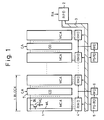
- Figure 1 schematically illustrates a fundamental constitution of the semiconductor memory device according to the present invention.
- reference 1 denotes a memory cell array (MCA) having a memory cell MC, for example, a dynamic type cell of one transistor and one capacitor, provided at each intersection between a plurality of word lines WL and a plurality of bit lines BL;
- reference 2 a row pre-decoding unit (RPD) which carries out a pre-decoding in response to a row address signal RA and outputs a plurality of row pre-decode signals;
- reference 3 a row pre-decode wiring (shown by a hatched portion) for transmitting the row pre-decode signals;
- reference 4 a row main decoder (RMD) which carries out a main decoding for selecting one of the plurality of word lines in response to a combination of a predetermined plurality of row pre-decode signals on the row pre-decode wiring;
- reference 5 a pseudo row decoder (PS, RD) constituted equivalently to the row main decoder;
- reference 6 a word line driver (WD) which starts its
- the pseudo row decoder 5 includes transistors having the same number of logic stages and the same gate length and gate width as those in the row main decoder 4. As stated later in detail, the pseudo row decoder 5 responds to a group of signals arriving last at the pseudo row decoder among the plurality of row pre-decode signals output on the row pre-decode wiring 3 and carries out a simulation of the main decoding of the row main decoder 4.
- Two memory cell arrays 1 and one column decoder 7 provided therebetween constitute one block.
- two row main decoders 4, one pseudo row decoder 5 and one word line driver 6 are allocated.
- the row pre-decoding unit 2 and the row pre-decode wiring 3 are allocated for a plurality of blocks.
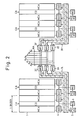
- FIG. 2 schematically illustrates an entire constitution of an embodiment of the present invention.
- FIG. 2 shows the case that the row address signal RA consists of seven address bits A0 - A6.
- References 2A - 2F denote row pre-decoders and references 3L, 3R denote row pre-decode wirings.
- the corresponding two row pre-decoders 2A, 2D; 2B, 2E; 2C, 2F carry out a pre-decoding in response to the address bits A0 , A1; A2 , A3; A4 , A5 , respectively.
- a plurality of memory cell arrays are divided into two regions (in the illustrated example, left and right sides) and six row pre-decoders 2A - 2F are provided between the two regions.
- a first half of the row pre-decoders 2A, 2B, 2C are allocated for the left region and a second half thereof 2D, 2E, 2F are allocated for the right region.
- One of the first and second halves is selected based on one address bit A6 ( A6 ) of the row address signal RA.
- the row pre-decoder 2C (2F) is located at the farthest position from the corresponding pseudo row decoder 5 among the row pre-decoders 2A - 2C (2D - 2F). Accordingly, the row pre-decode signals output from the row pre-decoder 2C (2F) arrive last at the pseudo row decoder 5 among all of the row pre-decode signals output on the row pre-decode wiring 3L (3R).
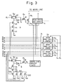
- FIG. 2 shows a concrete circuit constitution of main parts of the device shown in Fig. 2 with reference to Fig. 3.
- the illustrated example shows a circuit constitution corresponding to one block shown in Fig. 2.
- the row pre-decoders 2A - 2C respond to a combination of each logic level of the address bits A0, A1; A2 , A3; A4 , A5 , respectively, and output a group of four row pre-decode signals ⁇ 00 - ⁇ 03; ⁇ 10 - ⁇ 13; ⁇ 20 - ⁇ 23 , respectively.
- the pre-decoding is carried out so that, in a selection state, only one signal is at "H" level in each group consisting of four signals and the other three signals are at "L" level.
- the row main decoder 4 is constituted by two p-channel MOS transistors 41, 42 five n-channel MOS transistors 43 - 47 and an inverter 48.
- the transistors 43, 44, 45 are connected in series and a source of the transistor 43 is connected to a lower power supply line Vss (0 V).
- a drain of the transistor 45 is connected via the transistors 41, 42 connected in parallel with each other to a higher power supply line Vcc (5 V) and connected to an input end of the inverter 48.
- Each gate of the transistors 43, 44, 45 is connected to a signal line corresponding to one signal (in the example of the row main decoder 4 shown in the left side, ⁇ 00 , ⁇ 11 and ⁇ 22) among each group consisting of four signals on the row pre-decode wiring 3L, respectively.
- a gate of the transistor 41 receives the pre-charge signal ⁇ 1 , which is lowered to "L" level in a stand-by state and raised to "H” level in an active state.
- An output end of the inverter 48 is connected to a gate of the transistor 42 and connected via the transistor 46 to a gate of the transistor 47.
- the output signal of the inverter 48 is indicated by reference V2.
- a gate of the transistor 46 receives a signal ⁇ 2 , which has an enough level to turn ON the transistor 46.
- a source of the transistor 47 is connected to an output end of the word line driver 6 and a drain thereof is connected to a corresponding word line.
- the transistor 47 has a function of responding to a gate signal V1 of "H” level, transmitting a signal ⁇ 3 of "H" level output from the word line driver to the corresponding word line and boosting the level of the word line.
- the signal transmitted to the word line is indicated by reference ⁇ 4.
- the row main decoder 4 shown in the left side carries out a logic of NOT and AND (NAND) in response to three row pre-decode signals ⁇ 00 , ⁇ 11 and ⁇ 22.
- NAND NOT and AND
- the level at the input end of the inverter 48 is pulled down to the level of Vss ("L" level).
- the output signal V2 of the inverter 48 is brought to "H” level, which is applied via the transistor 46 to the gate of the transistor 47.
- the level of the word line is raised or boosted (i.e., selection of the word line).
- the pseudo row decoder 5 is constituted by two p-channel MOS transistors 51, 52, seven n-channel MOS transistors 53A - 53D, 54 - 56 and an inverter 57.
- the transistors 53A - 53D are connected in parallel and each source thereof is connected to the lower power supply line Vss. Each drain of the transistors 53A - 53D is connected via the transistor 54, the transistor 55 and the transistors 51, 52 connected in parallel with each other to the higher power supply line Vcc. A drain of the transistor 55 is connected to an input end of the inverter 57. Each gate of the transistors 53A - 53D is connected to each signal line corresponding to a group of signals (in the illustrated example, ⁇ 20 - ⁇ 23) arriving last at the pseudo row decoder 5 among the plurality of row pre-decode signals output on the row pre-decode wiring 3L, respectively.
- a gate of the transistor 51 receives the pre-charge signal ⁇ 1 and each gate of the transistors 54, 55 receives a signal ⁇ 6 having an enough level to turn ON the transistors 54, 55.
- An output end of the inverter 57 is connected to a gate of the transistor 52 and connected via the transistor 56 to the word line driver 6.
- a gate of the transistor 56 receives the same signal ⁇ 2 as that of the transistor 46.
- a signal appearing at the drain of the transistor 56 is indicated by reference ⁇ 5.
- the pseudo row decoder 5 includes transistors having the same number of logic stages as those in the row main decoder.
- the transistors 43, 44 and 45 correspond to the transistors 53A (or 53B - 53D), 54 and 55.
- each of the corresponding transistors has the same gate length and gate width. Therefore, the pseudo row decoder 5 can simulate a decoding operation of the row main decoder 4.
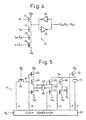
- Figure 4 illustrates a circuit constitution of the row pre-decoder shown in Fig. 3.
- the illustrated row pre-decoder is constituted by one p-channel MOS transistor 21 and three n-channel MOS transistors 22 - 24 connected in series between the two power supply lines Vcc, Vss, and a pair of inverters 25, 26 connected in parallel and in the reverse direction between a drain of the transistor 22 and the output end.
- the transistors 21 - 24 respond to the pre-charge signal ⁇ 1 , the address bit A6 , A0 or A0 , A1 or A1 , respectively.
- the row pre-decoder 2A is constituted by four circuits, each shown in Fig. 4.
- the constitution of the other row pre-decoders is the same as that of the row pre-decoder 2A and thus the explanation thereof is omitted.
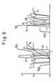
- Figure 5 illustrates a circuit constitution of the word line driver shown in Fig. 3 and Fig. 6 shows a timing chart of the operation thereof.
- the illustrated word line driver 6 is constituted by a clock generator 60 generating clock signals A - F with timings shown in Fig. 6 in response to the signal ⁇ 5 , one p-channel MOS transistor 62, eight n-channel MOS transistors 61, 63, 64, 66 - 70 and two MOS capacitors 65, 71.
- a gate of the transistor 61 is connected to the power supply line Vcc and a source thereof receives the clock signal A.
- the transistors 62, 63, 64 are connected in series between the power supply lines Vcc and Vss.
- a gate of the transistor 63 is connected to a drain of the transistor 61 (node N1) and each gate of the transistors 62, 64 receives the clock signal B.
- a drain of the transistor 64 (node N2) is connected to one end of the capacitor 65 and each gate of the transistors 66, 68.
- the transistors 66, 67 are connected in series between node N4 and the power supply line Vss.
- a drain of the transistor 67 (node N3) is connected to another end of the capacitor 65 and a gate thereof receives the clock signal C.
- the transistors 68, 69 are connected in series between node N4 and the power supply line Vss and a gate of the transistor 69 receives the clock signal D.
- the output signal ⁇ 3 of the word line driver 6 is obtained from the drain of the transistor 69.
- the node N4 is connected to a source of the transistor 70 and one end of the capacitor 71.
- a drain of the transistor 70 is connected to the power supply line Vcc and a gate thereof receives the clock signal E. Also, another end of the capacitor 71 receives the clock signal F.
- reference RAS denotes a low active row address strobe signal, which is generated by a controller (not shown) in response to the row address signal RA.
- the clock signal A is at "H” level (Vcc)
- the potential at node N1 is at “H” level (approximately Vcc).
- the clock signals B, C, D are at "H” level (Vcc)
- the potentials at nodes N2, N3 and the output signal ⁇ 3 are at "L” level (Vss), respectively.
- the clock signal E is at "H” level (Vcc + Vth, where Vth is a threshold level of the transistor 70)
- the potential at node N4 is at "H” level (Vcc).
- the output signal ⁇ 3 of "H” level is used for driving a selected word line by way of the row main decoder 4, as stated later.
- the output signal ⁇ 3 is lowered to "L" level.
- Figs. 7A and 7B show operational timings of each signal in the row main decoder 4 and the pseudo row decoder 5, respectively.
- the signal ⁇ 2 is first raised to the level of Vpc (Vcc + Vth, where Vth is a threshold level of the transistors 46, 56).
- the pre-charge signal ⁇ 1 is raised to "H” level and then the signal ⁇ 6 and the row pre-decode signals ⁇ 00 , ⁇ 11 are raised to "H” level.
- the row pre-decode signal ⁇ 22 is raised to "H” level.
- the transistors 43, 44, 45 are all brought to the ON state, the level at the input end of the inverter 48 is pulled down to the level of Vss ("L" level).
- the timing of the completion of the main decoding is determined by the arrival time of the signal ⁇ 22 contained in the group arriving last at the pseudo row decoder 5 among the plurality of row pre-decode signals output on the row pre-decode wiring 3L. Accordingly, the timing of the completion of the main decoding is the same as the timing at which the output signal ⁇ 5 of the pseudo row decoder 5 is raised to "H" level.
- the word line driver 6 starts its operation in response to the "H" level output signal ⁇ 5 of the pseudo row decoder 5. Namely, the wait time needed from when the row pre-decode signals are output until the operation of the word line driver 6 is started is determined depending on the operation of the pseudo row decoder 5. Therefore, it it possible to always realize the optimum wait time regardless of the nonuniformity of process, fluctuation of temperature, or the like. As a result, it is possible to perfectly exclude a possibility of an erroneous operation in the selection of word lines and prevent an unnecessary prolongation of the access time.
- the space occupied by wiring regions on a chip is relatively large compared with the space occupied by other integrated circuits.
- the space corresponding to the pseudo row decoder 5 is required, the input signal lines of the pseudo row decoder 5, i.e., the row pre-decode wiring 3, 3L, 3R, are common to the row main decoder 4. Namely, it is unnecessary to newly provide signal wiring regions. Therefore, it is possible to relatively reduce the space occupied by the entire device on the chip.
Landscapes
- Engineering & Computer Science (AREA)
- Microelectronics & Electronic Packaging (AREA)
- Computer Hardware Design (AREA)
- Dram (AREA)
- Read Only Memory (AREA)
Applications Claiming Priority (2)
| Application Number | Priority Date | Filing Date | Title |
|---|---|---|---|
| JP130361/88 | 1988-05-30 | ||
| JP63130361A JP2525455B2 (ja) | 1988-05-30 | 1988-05-30 | 半導体メモリ装置 |
Publications (3)
| Publication Number | Publication Date |
|---|---|
| EP0344632A2 true EP0344632A2 (fr) | 1989-12-06 |
| EP0344632A3 EP0344632A3 (fr) | 1991-09-11 |
| EP0344632B1 EP0344632B1 (fr) | 1993-12-15 |
Family
ID=15032539
Family Applications (1)
| Application Number | Title | Priority Date | Filing Date |
|---|---|---|---|
| EP89109502A Expired - Lifetime EP0344632B1 (fr) | 1988-05-30 | 1989-05-26 | Dispositif de mémoire à semi-conducteurs ayant un pseudo décodeur de rangée |
Country Status (5)
| Country | Link |
|---|---|
| US (1) | US4932000A (fr) |
| EP (1) | EP0344632B1 (fr) |
| JP (1) | JP2525455B2 (fr) |
| KR (1) | KR930006838B1 (fr) |
| DE (1) | DE68911381D1 (fr) |
Cited By (1)
| Publication number | Priority date | Publication date | Assignee | Title |
|---|---|---|---|---|
| EP0543269A3 (en) * | 1991-11-20 | 1993-10-27 | Fujitsu Ltd | Tracking pulse generator and ram with tracking precharge pulse generator |
Families Citing this family (4)
| Publication number | Priority date | Publication date | Assignee | Title |
|---|---|---|---|---|
| JP2661651B2 (ja) * | 1989-02-14 | 1997-10-08 | 沖電気工業株式会社 | 半導体記憶装置 |
| JP3299285B2 (ja) * | 1991-04-23 | 2002-07-08 | 株式会社日立製作所 | 半導体記憶装置 |
| KR100481857B1 (ko) | 2002-08-14 | 2005-04-11 | 삼성전자주식회사 | 레이아웃 면적을 줄이고 뱅크 마다 독립적인 동작을수행할 수 있는 디코더를 갖는 플레쉬 메모리 장치 |
| KR100582357B1 (ko) * | 2003-12-29 | 2006-05-22 | 주식회사 하이닉스반도체 | 로우디코딩을 효율적으로 할 수 있는 태그블럭을 구비하는반도체 메모리 장치 |
Family Cites Families (7)
| Publication number | Priority date | Publication date | Assignee | Title |
|---|---|---|---|---|
| JPS5644189A (en) * | 1979-09-19 | 1981-04-23 | Hitachi Ltd | Semiconductor memory |
| US4447895A (en) * | 1979-10-04 | 1984-05-08 | Tokyo Shibaura Denki Kabushiki Kaisha | Semiconductor memory device |
| JPS573289A (en) * | 1980-06-04 | 1982-01-08 | Hitachi Ltd | Semiconductor storing circuit device |
| JPS5968889A (ja) * | 1982-10-08 | 1984-04-18 | Toshiba Corp | 半導体記憶装置 |
| JPS6129488A (ja) * | 1984-07-20 | 1986-02-10 | Hitachi Micro Comput Eng Ltd | ダイナミツク型ram |
| JPS62202399A (ja) * | 1985-10-04 | 1987-09-07 | Mitsubishi Electric Corp | 半導体メモリ |
| JPS62180607A (ja) * | 1986-02-04 | 1987-08-07 | Fujitsu Ltd | 半導体集積回路 |
-
1988
- 1988-05-30 JP JP63130361A patent/JP2525455B2/ja not_active Expired - Lifetime
-
1989
- 1989-05-23 US US07/355,630 patent/US4932000A/en not_active Expired - Lifetime
- 1989-05-26 DE DE89109502T patent/DE68911381D1/de not_active Expired - Lifetime
- 1989-05-26 EP EP89109502A patent/EP0344632B1/fr not_active Expired - Lifetime
- 1989-05-29 KR KR1019890007169A patent/KR930006838B1/ko not_active Expired - Fee Related
Cited By (2)
| Publication number | Priority date | Publication date | Assignee | Title |
|---|---|---|---|---|
| EP0543269A3 (en) * | 1991-11-20 | 1993-10-27 | Fujitsu Ltd | Tracking pulse generator and ram with tracking precharge pulse generator |
| US5386150A (en) * | 1991-11-20 | 1995-01-31 | Fujitsu Limited | Tracking pulse generator and RAM with tracking precharge pulse generator |
Also Published As
| Publication number | Publication date |
|---|---|
| KR900019029A (ko) | 1990-12-22 |
| DE68911381D1 (de) | 1994-01-27 |
| KR930006838B1 (ko) | 1993-07-24 |
| US4932000A (en) | 1990-06-05 |
| JP2525455B2 (ja) | 1996-08-21 |
| EP0344632A3 (fr) | 1991-09-11 |
| JPH01300494A (ja) | 1989-12-04 |
| EP0344632B1 (fr) | 1993-12-15 |
Similar Documents
| Publication | Publication Date | Title |
|---|---|---|
| KR100316713B1 (ko) | 반도체 메모리 장치 및 이에 적합한 구동신호 발생기 | |
| US5600588A (en) | Data retention circuit and semiconductor memory device using the same | |
| JPH09180447A (ja) | 下位ワードライン駆動回路及びこれを利用した半導体メモリ装置 | |
| US4951259A (en) | Semiconductor memory device with first and second word line drivers | |
| JPS63244494A (ja) | 半導体記憶装置 | |
| JPH05266669A (ja) | シーケンス型ラッチ型行ラインリピータを有する半導体メモリ | |
| US5485426A (en) | Semiconductor memory device having a structure for driving input/output lines at a high speed | |
| US6055206A (en) | Synchronous semiconductor memory device capable of reducing power dissipation by suppressing leakage current during stand-by and in active operation | |
| IE53775B1 (en) | Semiconductor memory device | |
| US4618784A (en) | High-performance, high-density CMOS decoder/driver circuit | |
| JPH05334876A (ja) | メモリ行ライン選択用ラッチ型リピータを持った半導体メモリ | |
| US5818790A (en) | Method for driving word lines in semiconductor memory device | |
| JP2004199759A (ja) | 半導体記憶装置 | |
| KR960030409A (ko) | 반도체 기억장치 | |
| US6510094B2 (en) | Method and apparatus for refreshing semiconductor memory | |
| JPH10275468A (ja) | ダイナミック型ram | |
| US5848021A (en) | Semiconductor memory device having main word decoder skipping defective address during sequential access and method of controlling thereof | |
| US5359566A (en) | Dynamic random access memory | |
| EP0344632B1 (fr) | Dispositif de mémoire à semi-conducteurs ayant un pseudo décodeur de rangée | |
| KR101129147B1 (ko) | 컴파일드 메모리, asic 칩 및 컴파일드 메모리의 레이아웃 방법 | |
| US6229755B1 (en) | Wordline driving apparatus in semiconductor memory devices | |
| JP2016062625A (ja) | 半導体装置 | |
| US6243317B1 (en) | Semiconductor memory device which activates column lines at high speed | |
| US20020002696A1 (en) | Semiconductor memory device | |
| KR19990085199A (ko) | 칼럼 선택선 신호를 제어하여 데이터를 마스킹하는 반도체 메모리장치 및 이의 칼럼 디코더 |
Legal Events
| Date | Code | Title | Description |
|---|---|---|---|
| PUAI | Public reference made under article 153(3) epc to a published international application that has entered the european phase |
Free format text: ORIGINAL CODE: 0009012 |
|
| AK | Designated contracting states |
Kind code of ref document: A2 Designated state(s): DE FR GB |
|
| PUAL | Search report despatched |
Free format text: ORIGINAL CODE: 0009013 |
|
| AK | Designated contracting states |
Kind code of ref document: A3 Designated state(s): DE FR GB |
|
| 17P | Request for examination filed |
Effective date: 19920302 |
|
| 17Q | First examination report despatched |
Effective date: 19930217 |
|
| GRAA | (expected) grant |
Free format text: ORIGINAL CODE: 0009210 |
|
| AK | Designated contracting states |
Kind code of ref document: B1 Designated state(s): DE FR GB |
|
| PG25 | Lapsed in a contracting state [announced via postgrant information from national office to epo] |
Ref country code: DE Effective date: 19931215 |
|
| REF | Corresponds to: |
Ref document number: 68911381 Country of ref document: DE Date of ref document: 19940127 |
|
| ET | Fr: translation filed | ||
| PG25 | Lapsed in a contracting state [announced via postgrant information from national office to epo] |
Ref country code: GB Effective date: 19940526 |
|
| PLBE | No opposition filed within time limit |
Free format text: ORIGINAL CODE: 0009261 |
|
| STAA | Information on the status of an ep patent application or granted ep patent |
Free format text: STATUS: NO OPPOSITION FILED WITHIN TIME LIMIT |
|
| 26N | No opposition filed | ||
| GBPC | Gb: european patent ceased through non-payment of renewal fee |
Effective date: 19940526 |
|
| PGFP | Annual fee paid to national office [announced via postgrant information from national office to epo] |
Ref country code: FR Payment date: 20040510 Year of fee payment: 16 |
|
| PG25 | Lapsed in a contracting state [announced via postgrant information from national office to epo] |
Ref country code: FR Free format text: LAPSE BECAUSE OF NON-PAYMENT OF DUE FEES Effective date: 20060131 |
|
| REG | Reference to a national code |
Ref country code: FR Ref legal event code: ST Effective date: 20060131 |