EP0344736A2 - Synchrones Datenübertragungssystem mit grosser Geschwindigkeit - Google Patents
Synchrones Datenübertragungssystem mit grosser Geschwindigkeit Download PDFInfo
- Publication number
- EP0344736A2 EP0344736A2 EP89109790A EP89109790A EP0344736A2 EP 0344736 A2 EP0344736 A2 EP 0344736A2 EP 89109790 A EP89109790 A EP 89109790A EP 89109790 A EP89109790 A EP 89109790A EP 0344736 A2 EP0344736 A2 EP 0344736A2
- Authority
- EP
- European Patent Office
- Prior art keywords
- data
- functional unit
- machine cycle
- register
- signal
- Prior art date
- Legal status (The legal status is an assumption and is not a legal conclusion. Google has not performed a legal analysis and makes no representation as to the accuracy of the status listed.)
- Ceased
Links
Images



Classifications
-
- G—PHYSICS
- G06—COMPUTING OR CALCULATING; COUNTING
- G06F—ELECTRIC DIGITAL DATA PROCESSING
- G06F13/00—Interconnection of, or transfer of information or other signals between, memories, input/output devices or central processing units
-
- G—PHYSICS
- G06—COMPUTING OR CALCULATING; COUNTING
- G06F—ELECTRIC DIGITAL DATA PROCESSING
- G06F13/00—Interconnection of, or transfer of information or other signals between, memories, input/output devices or central processing units
- G06F13/38—Information transfer, e.g. on bus
- G06F13/42—Bus transfer protocol, e.g. handshake; Synchronisation
- G06F13/4247—Bus transfer protocol, e.g. handshake; Synchronisation on a daisy chain bus
- G06F13/4256—Bus transfer protocol, e.g. handshake; Synchronisation on a daisy chain bus using a clocked protocol
Definitions
- the present invention relates to high-speed data transfer between functional units and, more particularly, to a synchronous data transfer system capable of transferring data at high-speed between a plurality of pipelined functional unit stages for performing data processing at high speed, and incorporated in a highly integrated ASIC for a specific application.
- a conventional system for performing synchronous data transfer between functional units is generally arranged as shown in Fig. 1A.
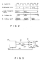
- data transfer between functional units 10 and 11 having an LSI arrangement as an ASIC is performed once for each machine cycle as represented by a machine cycle n shown in Fig. 2B.
- the transmitter functional unit 10 generates and transmits an available signal AVL 13 of logic "1" (high level) representing data transmission to the receiver functional unit 11.
- AVL 13 of logic "1" high level
- a positive logic is used.
- the receiver functional unit 11 is in a state capable of receiving data from the transmitter functional unit 10 in its machine cycle n as shown in Fig. 2E
- data from the transmitter functional unit 10 is loaded in a register 16 of the receiver functional unit 11 at the end point of the machine cycle n , i.e., at the boundary between the machine cycle n and the next machine cycle (n+1).
- a wait signal WAIT 14 of logic "1" representing this is output from the receiver functional unit 11 to the transmitter functional unit 10, as shown in Fig. 2E.
- the signal WAIT 14 representing whether the unit 11 is in a state capable of receiving data is generated inside the unit 11 under complex generation conditions.
- the conditions for outputting the signal WAIT 14 include whether the signal AVL 13 from the transmitter functional unit 10 is received and whether the receiver functional unit 11 is set in a state capable of receiving data in its current machine cycle. Therefore, it takes a long time period to determine the state of the signal WAIT 14 in the unit 11.
- the signal WAIT 14 cannot be determined at a considerably early timing of the machine cycle. For this reason, even if an LSI arrangement is adopted to each of the functional units 10 and 11 to increase its internal operational speed, it is difficult to shorten the rate the machine cycle.
- states of a data signal on a data transfer path 12 and the signals AVL 13 and WAIT 14 are those at the receiver side.
- the signal AVL 13 is set at logic ⁇ 0 ⁇ in a machine cycle prior to the machine cycle n .
- Fig. 2C shows a state in which the transmitter functional unit 10 does not send data.
- the transmitter functional unit 10 When the transmitter functional unit 10 receives and discriminates the signal WAIT 14 of logic "1" from the receiver functional unit 11 in the machine cycle (n+1) as shown in Fig. 2E, it successively sends the same data and the signal AVL 13 of logic "1" in the next machine cycle (n+2) as in the machine cycle (n+1).
- the receiver functional unit 11 When the receiver functional unit 11 is set in a state capable of receiving data from the transmitter functional unit 10 in the machine cycle (n+2), it cancels the signal WAIT 14 and loads the data in the register 16 at the end point of the machine cycle (n+2). In this case, two machine cycles are required to transfer one data.
- a time required for the stage 1 to determine whether the data can be received by the stage 2 is longer than a propagation time required for the signal AVL to reciprocate between the stages 1 and 2. For this reason, the rate of a clock cannot be increased, and therefore a time period of the machine cycle cannot be shortened.
- generation conditions of a signal representing whether data from the transmitter functional unit can be received by the receiver functional unit are not only complex but also include even a state of another functional unit connected to the output of the receiver functional unit. For this reason, a state of the signal cannot be determined at a relatively early timing in the machine cycle. Therefore, even if an internal operational speed of the functional unit is increased, it is difficult to shorten the machine cycle, and a data transfer rate between the functional units cannot be increased.
- an object of the present invention to provide a synchronous data transfer system capable of determining at a relatively early timing in a machine cycle whether data from a transmitter functional unit can be received by a receiver functional unit, thereby performing data transfer between the functional units at high speed.
- a system for synchronously transferring data between first and second functional units at high speed comprises the first and second functional units.
- the first functional unit includes transmission signal transmitting means, operating in synchronism with an input master clock signal defining a machine cycle, for generating and outputting a data transmission signal, representing that data is to be transferred, to the second functional unit at the start of a current machine cycle.
- the second functional unit includes state signal transmitting means, operating in synchronism with an input master clock signal, for generating, in accordance with only an internal state of the second functional unit, a reception state signal representing whether data can be received in the current machine cycle, and transmitting the reception state signal to the first function unit at the start of the first machine cycle.
- the first functional unit further comprises means for causing, in accordance with the reception state signal representing that the second functional unit cannot receive data in the current machine cycle, the transmitting means to continuously transmit the data transmission signal to the second functional unit even in a machine cycle next to the current machine cycle, transmission register means for latching internally generated data, and transmitting the held data to the second functional unit, and means for inhibiting, in accordance with the reception state signal representing that the second functional unit cannot receive data in the current machine cycle, a latching operation of the transmission register means in the current machine cycle.
- the second functional unit further comprises first register means for receiving data from the first function unit at a predetermined timing in the current machine cycle, second register means for selectively receiving data from the first register means, and first state holding means for representing that effective data is held in the first register means.
- the second functional unit further comprises means for inhibiting, in accordance with the reception state signal representing that the second function unit cannot receive data in the current machine cycle, reception by the first register means in the current machine cycle, and means for permitting, in accordance with a state control signal representing that the second function unit can receive data, the second register means to receive data from the first register means at the start of the machine cycle next to the current machine cycle.
- the second functional unit further comprises means for inhibiting, in accordance with the state control signal representing that the second functional unit cannot receive data, the second register means from receiving data in the next machine cycle, and means for generating a signal representing that the second register means has latched the data.
- data transmitted from the first functional unit is held in the first register means of the second functional unit (receiver functional unit) at a predetermined timing in the middle of a machine cycle, and at the same time the state of a specific interface signal from the transmitter functional unit is held in the first state holding means, thereby representing that effective data is held in the first register means.
- the first register means is set in a latching operation inhibit state at the end point of the machine cycle.
- information representing whether data can be received is transferred to the transmitter functional unit in the next machine cycle.
- the receiver function unit can determine at an early timing in the machine cycle whether data can be received from the transmitter functional unit. Therefore, even if a signal transmission rate (operation of an interface of the functional unit) between the functional units is much lower than an internal operational speed of each functional unit, a clock rate can be increased and a machine cycle can be shortened to substantially correspond to a time period required for a signal to propagate in one direction of an interface, thereby increasing an operational speed of the overall system.
- an inhibit state is set at the end point of a machine cycle n , the latching operation of the first register is inhibited. Therefore, the content of the first register means is not updated even after the predetermined timing in the middle of the next machine cycle (n+1), and the held data is kept held. That is, the first register means contributes to a clock skew countermeasure and also serves as a data buffer when the second register means is not permitted to receive data.
- a method of synchronously transferring data between first and second functional units at high speed comprises: generating and outputting a data transmission signal, representing that data is to be transferred, from the first to second functional unit in synchronism with a master clock signal at the start of a current machine cycle, the master clock defining the machine cycle; and generating, in the second functional unit, a reception state signal representing that data can be received in the current machine cycle, in synchronism with the master clock signal and independently of the data transmission signal, and transmitting the reception state signal to the first functional unit at the start of the first machine cycle.
- the signal for transmitting information, representing whether data from the transmitter functional unit can be received by the receiver functional unit, to the transmitter functional unit can be determined at a relatively early timing in a machine cycle in accordance with only an internal state of the receiver function unit regardless of an external input. Therefore, a clock rate can be increased and a machine cycle can be shortened to substantially correspond to a time period required for a signal to propagate in one direction between the functional units, thereby increasing a data transfer rate between the functional units.
- two stages of registers are used to receive data from the transmitter functional unit, and the register at the front stage is strobed at a predetermined timing in the middle of the machine cycle. Therefore, not only the register at the front stage can serve as a data buffer when the register at the second stage cannot receive data, but also a stable operation is assured even if a clock skew between the functional units is increased.
- a synchronous data transfer system An arrangement of a synchronous data transfer system according to an embodiment of the present invention will be described below with reference to Fig. 3.
- functional units 20 and 21 are LSI chips using, for example, CMOS large-scale ASICs and are connected with each other via a data transfer path 22.
- a clock CLK 25 is supplied to the functional units 20 and 21 in order to define timings of an internal operations of the functional units 20 and 21 and especially to synchronize data transfer timings.
- the functional units 20 and 21 take over portions of processing operations to be executed by the overall system.
- the transmitter functional unit 20 transfers, e.g., 1-byte data representing a result of its allotted processing operation in parallel to the receiver functional unit 21 in a certain machine cycle via the data transfer path 22. Simultaneously with data transmission, the unit 20 generates and transmits a transfer control signal (available signal AVL) 23 as an interface signal to the receiver functional unit 21. Signal AVL 23 represents that the data is transmitted onto the data transfer path 22.
- the unit 21 generates, independently of the signal AVL 23, a transfer control signal (wait signal WAIT) 24 as the interface signal and transmits the signal WAIT 24 to the transmitter functional unit 20. Signal WAIT 24 represents whether or not the transmitted data can be received in the machine cycle.
- the receiver functional unit 21 When the receiver functional unit 21 is in a state capable of receiving data, it receives the transmission data from the transmitter functional unit 20 in this machine cycle, and executes a processing operation assigned to the unit in the next machine cycle. A function of transmitting a result of the assigned processing operation to a functional unit (not shown) at the next stage may be arbitrarily provided.
- a register 26 in the receiver functional unit 21 latches the transmission data from the transmitter functional unit 20 at a predetermined timing of the current machine cycle, e.g., at a timing for a 1/4 machine cycle before the end point of the current machine cycle, i.e., the start point of the next machine cycle.
- a flip-flop (to be referred to as an F/F hereinafter) 27 is, e.g., a D-type F/F for latching the signal AVL 23 at the same timing as that of the register 26.
- a register 28 latches the data held in the register 26 at the timing of the end point of the current machine cycle.
- a D-type F/F 29 is set when the F/F 27 has been set and the data held in the register 26 is not permitted to be loaded in the register 28.
- the F/F 29 is set, data transfer from the register 26 to the register 28 is inhibited, and an active signal WAIT 24, i.e., a signal WAIT 24 of logic "1" is generated.
- Fig. 4 is a block diagram showing in detail internal arrangements of the transmitter and receiver functional units 20 and 21 shown in Fig. 3. Note that the same reference numerals as in Fig. 3 denote the same parts in Fig. 4.
- a clock generator 47 of the transmitter function unit 20 generates strobe clock pulses $M1 and $S1 for defining a timing in accordance with a clock 25.
- An AND gate 45 receives a signal 31 for clock-enabling a register 32 which signal is generated inside. An inverted output from an F/F 42 to be described later is supplied to the AND gate 45. An output from the AND gate 45 is supplied to a clock enable terminal E of the register 32.
- the transmitter functional unit 20 is in an output enable state
- the F/F 42 is in a reset state, and its Q output signal is at logic ⁇ 0 ⁇ .
- the AND gate 45 is enabled to output the signal 31 to the clock enable terminal E of the register 32.
- the signal 31 is active (at logic "1") when the data generated in the transmitter functional unit 20 is effective and at the same time the unit 20 is in the output enable state.
- the register 32 receives the pulse $M1 from the clock generator 47 and a signal of logic "1" at its clock input terminal and clock enable terminal E, respectively, it latches the data generated in the transmitter functional unit 20 via a path 30. As a result, the data latched by the register 32 is output onto the data transfer path 22 via an output driver D1.
- the output from the AND gate 45 is also supplied to one input terminal of an OR gate 44.
- An output signal from an AND gate 43 is supplied to the other input terminal of the OR gate 44.
- An output signal from the OR gate 44 is supplied to a D input terminal of a D-type F/F 46.
- the pulse $M1 is supplied from the clock generator 47 to the clock input terminal of the F/F 46. Therefore, the F/F 46 sets a D input to a Q output in synchronism with a timing of the pulse $M1, i.e., at the same timing at which the data is loaded in the register 32. As a result, the Q output from the F/F 46 is output as a signal AVL via a driver D2.
- the signal WAIT 24 from the receiver functional unit 21 is supplied to the D input terminal of the F/F 46.
- the signal WAIT 24 is set in the F/F 42 at a timing of the pulse $S1 in the same machine cycle as the above pulse $M1.
- the Q output from the F/F 42 is inverted and supplied to the AND gate 45.
- the AND gate 45 is disabled to inhibit the signal 31 from being transmitted to the clock enable input terminal E of the register 32.
- an operation of loading new data in the register 32 is inhibited, and the data held in the register 32 in the current machine cycle is kept held therein in the next machine cycle. Therefore, the data on the data transfer path 22 does not change.
- the transmitter functional unit 20 determines that the transmitted data cannot be received by the receiver functional unit 21 and successively sends the same data in the next machine cycle.
- the Q output from the F/F 42 is also supplied to the AND gate 43 together with the Q output from the F/F 46.
- the output signal from the AND gate 43 is supplied to the OR gate 44 together with the output signal from the AND gate 45.
- the output signal from the OR gate 44 is supplied to the D input terminal of the F/F 46. Therefore, when the F/F 46 is already set, i.e., its Q output signal is at logic "1" and at the same time the Q output signal from the F/F 42 is at logic "1", the output signal from the AND gate 43 is set at logic "1". As a result, since the F/F 46 is kept set in the next machine cycle, the signal AVL 23 of logic "1" is maintained in the next machine cycle.
- the Q output from the F/F 42 can also be used as a clock enable signal for various registers in the transmitter functional unit 20, e.g., an input signal for a logic circuit (not shown) for generating the signal 31.
- the Q output from the F/F 42 is updated by the signal WAIT in synchronism with the timing of the pulse $S1. Therefore, in this embodiment, only a 1/4 machine cycle is left until a timing of the pulse $M1 in the next machine cycle.
- a clock enable signal system is generally designed to shorten a signal propagation time, no problem is posed.
- a pulse generator 48 in the receiver functional unit 21 generates strobe clock pulses $M2 and $S2 for defining a timing in accordance with the clock CLK 25.
- the pulses $M2 and $S2 are slightly shifted from the pulses $M1 and $S1.
- the data on the data transfer path 22 is supplied to the input terminal of the register 26 of the receiver functional unit 21.
- the Q output signal from the F/F 29 is inverted by an inverter 41 and supplied to the clock enable input terminal E of the register 26.
- the pulse $S2 is supplied from the pulse generator 48 to the clock input terminal of the register 26.
- the data on the path 22 is latched by the register 26 at a timing of the pulse $S2 in the same machine cycle in which the transmitter functional unit 20 sends the data to the path 22.
- the latched data is output to the register 28.
- the signal AVL 23 from the transmitter functional unit 20 is supplied to the D input terminal of the F/F 27 of the receiver functional unit 21.
- the pulse $S2 is also supplied from the clock generator 48 to the clock input terminal of the F/F 27. Therefore, the signal AVL 23 is latched by the F/F 27 at the same timing as the data is latched by the register 26. As a result, when the signal AVL is at logic "1", the F/F 27 is set. Setting of the F/F 27 represents that the new data is latched by the register 26.
- the data held in the register 26 is supplied to the input terminal of the register 28.
- a signal 35 representing whether or not the data held in the register 26 can be received by the register 28 in the receiver functional unit 21 is supplied to the clock enable input terminal E of the register 28.
- the pulse $M2 is supplied from the clock generator 48 to the clock input terminal of the register 28. Therefore, when the register 28 can receive the data, i.e., when the signal 35 is at logic "1", the data held in the register 26 is loaded in the register 28 at a timing of the pulse $M2 in a machine cycle next to the machine cycle to which the above pulse $S2 belongs.
- the signal 35 is at logic ⁇ 0 ⁇ , and a latching operation of the register 28 is inhibited.
- the data held in the registers 26 and 28 are kept unchanged.
- a logic circuit comprising a combination circuit for performing data processing to data from the register 26 can be inserted between the registers 26 and 28, if necessary.
- a time interval from the timing of the pulse $S2 to the timing of the pulse $M2 in the next machine cycle is shorter than the machine cycle, i.e., about a 1/4 machine cycle in this embodiment. Therefore, the number of logic stages must be naturally decreased.
- the Q output signals from both the F/Fs 27 and 29 are supplied to an OR gate 37.
- An output signal from the OR gate 37 is supplied to the AND gate 38 together with an inverted signal of the signal 35.
- An output signal 40 from the OR gate 37 used in the receiver functional unit 21 serves the same purpose as that of the output from the F/F 42 in the transmitter functional unit 20.
- the signal 40 represents that data to be loaded next in the register 28 is held in the register 26.
- An output signal from the AND gate 38 is supplied to the D input terminal of the F/F 29. Therefore, the signal 35 is gated by the output signal from the OR gate 37.
- the pulse $M2 from the clock generator 47 is supplied to the clock input terminal of the F/F 29.
- the signal 35 is set in the F/F 27 at a timing of the pulse $M2.
- the Q output signal from the F/F 27 is already at logic "1" and the signal 35 is at logic ⁇ 0 ⁇
- the output signal of logic "1" from the AND gate 38 is supplied to the D input terminal of the F/F 29.
- the F/F 29 is set at logic "1" at a timing of the pulse $M2 in a machine cycle subsequent to that of the pulse $S2. That is, when the register 28 cannot receive the data held in the register 26, the F/F 29 is set.
- the Q output signal of logic "1" from the F/f 29 is supplied as an active signal WAIT 24 to the transmitter functional unit 20 via an output driver D3 in this machine cycle.
- the Q output signal of logic "1" from the F/F 29 is level-inverted by the inverter 41 and supplied to the clock enable input terminal E of the register 26. As a result, a loading operation of new data to the register 26 is inhibited, and the currently-registered data is kept held therein.
- the signal WAIT 24 is set at logic ⁇ 0 ⁇ in the same machine cycle, and the F/F 42 of the transmitter functional unit 20 is reset at the timing of the pulse $S1 in this machine cycle.
- the AND gate 45 is enabled, and a loading operation of new transmission data in the register 32 at the timing of the pulse $M1 in the next machine cycle is enabled.
- the signal 31 When data N is generated in a machine cycle before the machine cycle n in the transmitter functional unit 20 and the unit 20 is in a transmission enable state, the signal 31 becomes active (i.e., is set at logic "1"). At this time, if the F/F 42 is in a reset state, since the gate 45 is in an enable state, the signal 31 passes through the gate 45 and is supplied to the clock enable input terminal E of the register 32. The pulse $M1 of machine cycle n is supplied to the clock input terminal of the register 32. Therefore, the data N is latched by the register 32 via the path 30 at a timing of the pulse $M1 in the machine cycle n and is output from the transmitter functional unit 20 to the receiver functional unit 21 via the data transfer path 22.
- the signal 31 is also supplied to the D input terminal of the D-type F/F 46 via the OR gate 44.
- the pulse $M1 is supplied to the clock input terminal of the F/F 46. Therefore, the signal 31 is set in the F/F 46 at the same timing of the pulse $M1 as the data N is loaded in the register 32.
- a signal AVL 23 of logic "1" representing that the data N is transmitted is output to the receiver functional unit 21 via the driver D2.
- the transmitter functional unit 20 generates data (N+1) in the machine cycle n .
- the signal WAIT 24 of logic ⁇ 0 ⁇ is output from the F/F 29 to the transmitter functional unit 20 and strobed at the timing of the pulse $S1 in the machine cycle n , and the F/F 42 is reset.
- the data N on the data transfer path 22 is supplied to the input terminal of the register 26 of the receiver functional unit 21, and the signal AVL 23 is supplied to the D input terminal of the F/F 27 of the unit 21.
- the pulse $S2 is supplied from the clock generator 48 to the clock input terminals of the register 26 and the F/F 27.
- the Q output signal from the F/F 29 is inverted by the inverter 41 and supplied to the clock enable input terminal E of the register 26.
- the F/F 29 is in a reset state, i.e., when the signal WAIT is at logic ⁇ 0 ⁇ the data on the path 22 is latched by the register 26 at a timing of the pulse $S2 in the machine cycle n , i.e., at a timing earlier than the end point of the machine cycle n by a 1/4 machine cycle.
- the signal AVL 23 of logic "1" is latched by the F/F 27, and the F/F 27 is set. Setting of the F/F 27 represents that the new data is held in the register 26.
- the data N held in the register 26 is supplied to the input terminal of the register 28.
- the signal (significant at logic "1") 35 representing that the data N held in the register 26 can be received by the register 28 is supplied to the clock enable input terminal E of the register 28 of the receiver functional unit 21.
- the signal 35 is at logic ⁇ 0 ⁇ .
- the clock enable input terminal E of the register 28 is set at logic ⁇ 0 ⁇ , a latching operation of the register 28 is inhibited.
- An inverted signal of the signal 35 gated by the Q output from the F/F 27 via the OR gate 37 is latched by the F/F 29 at the timing of the pulse $M2 in the machine cycle (n+1), and the F/F 29 is set.
- the Q output signal of logic "1" from the F/F 29 is supplied as an active signal WAIT 24 to the transmitter functional unit 20 via the output driver D3.
- the F/F 42 Since the F/F 42 has been reset in the transmitter functional unit 20 at the timing of pulse $S1 in the machine cycle n , the data (N+1) generated in the machine cycle n and the signal AVL are transmitted from the unit 20 to the receiver functional unit 21 at the timing of $M1 of the machine cycle (n+1).
- the Q output signal of logic "1" from the F/F 29 is inverted by the inverter 41 and supplied to the clock enable input terminal E of the register 26, and the input terminal E is set at logic ⁇ 0 ⁇ . As a result, a loading operation of the register 26 is inhibited, and the data N is kept held even in a machine cycle (n+1).
- the signal WAIT 24 is supplied to the D input terminal of the F/F 42 and latched by the F/F 42 at the timing of the pulse $S1. For this reason, when the signal WAIT 24 of logic "1" is sent from the unit 20, the F/F 42 is set at the timing of the pulse $S1 in the machine cycle (n+1).
- the Q output signal from the F/F 42 is supplied to the AND gate 45.
- the AND gate 45 is disabled, and transmission of the clock enable signal 31 to the clock enable input terminal E of the register 32 is inhibited.
- the D input of the F/F 29 is set at logic ⁇ 0 ⁇ , since the Q output from the F/F 29 is at logic "1", and the F/F 29 is reset at the timing of the pulse $M2 in the machine cycle (n+2).
- the data held in the register 26 is loaded in the register 28.
- the F/F 29 is reset, loading operation inhibition of the register 26 is released, and the data (N+1) successively transmitted from the transmitter functional unit 20 onto the path 22 is loaded in the register 26 at the timing of the pulse $S2 in the machine cycle (n+2).
- the F/F 27 is set to indicate that the new data is loaded in the register 26.
- the signal WAIT 24 is set at logic ⁇ 0 ⁇ in the machine cycle (n+2), and the F/F 42 is reset at the timing of the pulse $S1 in the machine cycle (n+2).
- the AND gate 45 is enabled so that the new data can be loaded in the register 32 at the timing of the pulse $M1 in a machine cycle next to the machine cycle (n+2).
- the register 26 contributes to a clock skew countermeasure (well known to those skilled in the art and therefore a detailed description thereof will be omitted). That is, even if a clock skew is considerably increased (in this embodiment, close to a 1/8 machine cycle on the basis of the reference) between the functional units 20 and 21, the register 26 can stably operate.
- the register 26 also serves as a data buffer when the register 28 is set in a state not capable of receiving data.
- the signal WAIT 24 of logic "1" representing that the register 28 cannot receive the data N held in the register 26 in the machine cycle (n+1) and therefore the register 26 cannot receive the data (N+1) transmitted to the data transfer path 22 in the machine cycle (n+1), is output to the transmitter functional unit 20 in accordance with the output from the F/F 29.
- a state of the signal WAIT 24 is determined before the machine cycle (n+2) is started, i.e., at the timing of the pulse $S1 in the machine cycle (n+1) in the receiver functional unit 21.
- a clock rate can be increased and a machine cycle can be shortened to substantially correspond to a time period required for a signal to propagate in one direction in the interface (in this embodiment until the propagation time occupies close to a 3/4 machine cycle), thereby increasing an operation speed of the overall system.
- data transfer is performed in one direction from the functional unit 20 to 21.
- the functional units 20 and 21 can have a similar circuit arrangement with both transmitting and receiving functions, and the data transfer path 22 can have an arrangement capable of performing bidirectional data transfer.
- the register 26 and the inverter 41 may be omitted.
- F/F 27 may be triggered by the pulse $M2.
- the signal WAIT can be generated at the start of a certain machine cycle regardless of the signal AVL and without waiting for a signal WAIT from another functional unit if it is connected to the functional unit 21. Therefore, a clock rate can be increased to increase the data transfer speed.
- the present invention can also be applied, in combination with conventional techniques, to a data transfer path of a "bus" type in which the number of transmitter functional units is increased.
- functional units 20-1 and 20-2 scramble for, simultaneously with data transfer in a machine cycle n , a data transmission right in the next machine cycle (n+1), and the functional unit which obtained the transmission right transmits data to a receiver functional unit 21-1 or 21-2 as described above.
- the transmitter functional unit 20-1 is to transmit data to the receiver functional unit 21-1
- data transfer is controlled by a signal WAIT not from the functional unit 21-2 but from the functional unit 21-1.
- each of the functional units 20 and 21 is an LSI chip using a CMOS large-scale ASIC.
- a GaAs LSI chip can be similarly used.
- the GaAs LSI chip is utilized in a field requiring a high speed. For this reason, when the GaAs LSI chip is used as a functional unit, a ratio between an internal operational speed of the chip and a signal propagation speed outside the chip is very large. Therefore, the present invention has a great effect in this application.
- the pulses $S1 and $S2 need not be generated at a timing a 1/4 machine cycle before the end point of the machine cycle but may be generated at any predetermined timing in the middle of the machine cycle.
- the timing can be arbitrarily determined in consideration of a system design and a functional unit design on the basis of a signal propagation speed between functional units, an internal operational speed of the unit, and the like.
- a small amount of logic circuits can be inserted between the register (32) and the F/Fs (46 and 29) to which interface signals (e.g., the data signal, the signal AVL, and the signal WAIT) are transmitted, and the output drivers (DI to D3).
- interface signals e.g., the data signal, the signal AVL, and the signal WAIT
- the output drivers DI to D3
- This arrangement is adopted when, for example, the output data 34 in Fig. 6 from the register 28 is significant in at least one machine cycle (the data 34 can be continuously significant in a subsequent machine cycle by setting the signal 35 at logic ⁇ 0 ⁇ ) and a synchronized signal representing "the output data 34 from the register 28 is significant" is required in designing the receiver functional unit 21.
- the output signal from the OR gate 37 for example, can be synchronized and used at the timing of the pulse $M2.
- the internal arrangement of the unit 21 shown in Fig. 4 may be partially altered as shown in Fig. 6.
- an output signal from an OR gate 37 to which a Q output signal from a flip-flop (F/F) 27 and an output signal from an AND gate 54 to be described later are supplied, is supplied to a D input terminal of a D-type F/F 50.
- a pulse $M2 is supplied to a clock input terminal of the F/F 50. Therefore, when the F/F 27 is set, the Q output signal of logic "1" is supplied from the F/F 27 to the D input terminal of the F/F 50 via the OR gate 37, thereby setting the F/F 50 at a timing of the pulse $M2. As a result, a Q output signal 51 of logic "1" is supplied from the F/F 50.
- This signal can be used as a synchronized signal 51 representing "output data 34 from a register 28 is significant" in a functional unit.
- the signal 35 is set at logic "1".
- the signal 35 inverted by an inverter 52 is latched by an F/F 53 at the timing of the pulse $M2.
- a Q output signal from the F/F 53 together with the Q output signal from the F/F 50 are supplied to the AND gate 54.
- the output signal from the AND gate 54 has the same logical meaning as that of the Q output signal from the F/F 29 shown in Fig.
- the register having the clock enable input terminal E (in the case of an ASIC, a register macrocell capable of clock enable) is applied.
- a register of this type is not used, however, a system for gating with a pulse similar to a clock pulse in place of the strobe clock pulses $M and $S can be used, although it is not desirable in timing design. That is, a gated clock designing method, in which the leading or trailing edge of a pulse of a negative pulse train set at logic ⁇ 0 ⁇ from the pulse $S to $M as shown in Fig. 5A is used as a timing of the pulses $M and $S, may be applied.
- strobe timings of the register 26 and the F/Fs 27 and 42 which receive the interface signals first are preferably located at the center of the machine cycle as shown in timing charts of Figs. 7A to 7I. In this case, however, only clocks of the pulses $S1 and $S2 are shifted to the center of the machine cycle, and basic operations are similar to those shown in Figs. 4 and 5A to 5G.
- the present invention can be applied to a system for performing data transfer in a pipeline manner in which a plurality of functional units 60, 61, 62,..., having a transmitting function of the transmitter functional unit 21 and a receiving function of the receiver functional unit 20 both shown in Fig. 4, are pipelined.
- a data buffer (the register 26 shown in Figs. 3 and 4) is provided at a receiving side of each of the functional unit 60, 61, 62,... Therefore, even when the functional unit 62 cannot receive data, for example, data transfer can be performed by exchanging interface signals only between the functional units 61 and 60. That is, no signal to be propagated through three or more functional unit stages is present in one machine cycle. As a result, a system clock rate can be increased as when the number of functional unit stages is small.
Landscapes
- Engineering & Computer Science (AREA)
- Theoretical Computer Science (AREA)
- Physics & Mathematics (AREA)
- General Engineering & Computer Science (AREA)
- General Physics & Mathematics (AREA)
- Information Transfer Systems (AREA)
- Synchronisation In Digital Transmission Systems (AREA)
- Multi Processors (AREA)
Applications Claiming Priority (2)
| Application Number | Priority Date | Filing Date | Title |
|---|---|---|---|
| JP131515/88 | 1988-05-31 | ||
| JP63131515A JPH01302459A (ja) | 1988-05-31 | 1988-05-31 | 高速同期式データ転送方式 |
Publications (2)
| Publication Number | Publication Date |
|---|---|
| EP0344736A2 true EP0344736A2 (de) | 1989-12-06 |
| EP0344736A3 EP0344736A3 (de) | 1991-07-24 |
Family
ID=15059846
Family Applications (1)
| Application Number | Title | Priority Date | Filing Date |
|---|---|---|---|
| EP19890109790 Ceased EP0344736A3 (de) | 1988-05-31 | 1989-05-31 | Synchrones Datenübertragungssystem mit grosser Geschwindigkeit |
Country Status (3)
| Country | Link |
|---|---|
| EP (1) | EP0344736A3 (de) |
| JP (1) | JPH01302459A (de) |
| KR (1) | KR930001589B1 (de) |
Cited By (4)
| Publication number | Priority date | Publication date | Assignee | Title |
|---|---|---|---|---|
| EP0579389A1 (de) * | 1992-06-26 | 1994-01-19 | Sun Microsystems, Inc. | Zum Sender synchronisierter Bus ohne metastabilen Zustand |
| EP0590212A1 (de) * | 1992-09-30 | 1994-04-06 | International Business Machines Corporation | Synchronisationseinrichtung für ein synchrones Datenkommunikationssystem |
| US5442658A (en) * | 1993-09-07 | 1995-08-15 | International Business Machines Corporation | Synchronization apparatus for a synchronous data processing system |
| WO2000014875A1 (en) * | 1998-09-04 | 2000-03-16 | Sun Microsystems, Inc. | Circuit for distribution of clock signals using muller elements |
Family Cites Families (4)
| Publication number | Priority date | Publication date | Assignee | Title |
|---|---|---|---|---|
| US4112490A (en) * | 1976-11-24 | 1978-09-05 | Intel Corporation | Data transfer control apparatus and method |
| US4476527A (en) * | 1981-12-10 | 1984-10-09 | Data General Corporation | Synchronous data bus with automatically variable data rate |
| DE3751609T2 (de) * | 1986-09-01 | 1996-07-04 | Nippon Electric Co | Datenprozessor mit Hochgeschwindigkeitsdatenübertragung. |
| WO1988008574A1 (fr) * | 1987-04-28 | 1988-11-03 | Fujitsu Ten Limited | Procede et appareil pour le transfert de donnees |
-
1988
- 1988-05-31 JP JP63131515A patent/JPH01302459A/ja active Pending
-
1989
- 1989-05-30 KR KR1019890007231A patent/KR930001589B1/ko not_active Expired - Fee Related
- 1989-05-31 EP EP19890109790 patent/EP0344736A3/de not_active Ceased
Cited By (6)
| Publication number | Priority date | Publication date | Assignee | Title |
|---|---|---|---|---|
| EP0579389A1 (de) * | 1992-06-26 | 1994-01-19 | Sun Microsystems, Inc. | Zum Sender synchronisierter Bus ohne metastabilen Zustand |
| US5392422A (en) * | 1992-06-26 | 1995-02-21 | Sun Microsystems, Inc. | Source synchronized metastable free bus |
| EP0590212A1 (de) * | 1992-09-30 | 1994-04-06 | International Business Machines Corporation | Synchronisationseinrichtung für ein synchrones Datenkommunikationssystem |
| US5442658A (en) * | 1993-09-07 | 1995-08-15 | International Business Machines Corporation | Synchronization apparatus for a synchronous data processing system |
| WO2000014875A1 (en) * | 1998-09-04 | 2000-03-16 | Sun Microsystems, Inc. | Circuit for distribution of clock signals using muller elements |
| US6304125B1 (en) | 1998-09-04 | 2001-10-16 | Sun Microsystems, Inc. | Method for generating and distribution of polyphase clock signals |
Also Published As
| Publication number | Publication date |
|---|---|
| KR930001589B1 (ko) | 1993-03-05 |
| KR890017616A (ko) | 1989-12-16 |
| EP0344736A3 (de) | 1991-07-24 |
| JPH01302459A (ja) | 1989-12-06 |
Similar Documents
| Publication | Publication Date | Title |
|---|---|---|
| US5600824A (en) | Clock generating means for generating bus clock and chip clock synchronously having frequency ratio of N-1/N responsive to synchronization signal for inhibiting data transfer | |
| US5654988A (en) | Apparatus for generating a pulse clock signal for a multiple-stage synchronizer | |
| US5019966A (en) | Dual processors using busy signal for controlling transfer for predetermined length data when receiving processor is processing previously received data | |
| US4503490A (en) | Distributed timing system | |
| KR101089153B1 (ko) | 상이한 클록 도메인 간에서의 데이터 신호 전송 방법 및 집적 회로 | |
| US5140680A (en) | Method and apparatus for self-timed digital data transfer and bus arbitration | |
| JPH0786525B2 (ja) | 診断回路 | |
| US5408641A (en) | Programmable data transfer timing | |
| EP0375794A1 (de) | Methode zur Synchronisierung von Signalen, die auf verschiedenen Chips mit On-Chip-Taktgebern verschiedener Frequenz erzeugt werden | |
| JP2579237B2 (ja) | フロースルーラッチ回路を有する状態素子回路、該状態素子回路を有するvlsi回路、及びラッチをマスタースレーブフリップフロップの機能的代替物として作動する方法 | |
| US6425088B1 (en) | Method of the apparatus for transferring data between circuits | |
| EP0225512B1 (de) | Synchronisierschaltung für digitalen, freilaufenden Taktgeber | |
| US7590146B2 (en) | Information processing unit | |
| EP0651319B1 (de) | System für Datentransfer | |
| US5726595A (en) | Circuit for coupling an event indication signal across asynchronous time domains | |
| KR930001589B1 (ko) | 고속동기식 데이타 전송 시스템 및 그 전송방법 | |
| EP0110104A2 (de) | Flankengetriggerte Kippschaltung | |
| US4962474A (en) | LSSD edge detection logic for asynchronous data interface | |
| US6255869B1 (en) | Method and apparatus for system resource negotiation | |
| US5249154A (en) | Data access controller and method | |
| US6654844B1 (en) | Method and arrangement for connecting processor to ASIC | |
| JPH04233014A (ja) | コンピュータ・システム | |
| JP2000353939A (ja) | クロック信号同期式フリップフロップ回路 | |
| JPH0756645B2 (ja) | データ処理装置 | |
| JP2581041B2 (ja) | デ−タ処理装置 |
Legal Events
| Date | Code | Title | Description |
|---|---|---|---|
| PUAI | Public reference made under article 153(3) epc to a published international application that has entered the european phase |
Free format text: ORIGINAL CODE: 0009012 |
|
| 17P | Request for examination filed |
Effective date: 19890531 |
|
| AK | Designated contracting states |
Kind code of ref document: A2 Designated state(s): DE FR GB |
|
| PUAL | Search report despatched |
Free format text: ORIGINAL CODE: 0009013 |
|
| AK | Designated contracting states |
Kind code of ref document: A3 Designated state(s): DE FR GB |
|
| 17Q | First examination report despatched |
Effective date: 19940407 |
|
| STAA | Information on the status of an ep patent application or granted ep patent |
Free format text: STATUS: THE APPLICATION HAS BEEN REFUSED |
|
| 18R | Application refused |
Effective date: 19951119 |