EP0344866A2 - Detektionsvorrichtung für Strahlung - Google Patents
Detektionsvorrichtung für Strahlung Download PDFInfo
- Publication number
- EP0344866A2 EP0344866A2 EP89201402A EP89201402A EP0344866A2 EP 0344866 A2 EP0344866 A2 EP 0344866A2 EP 89201402 A EP89201402 A EP 89201402A EP 89201402 A EP89201402 A EP 89201402A EP 0344866 A2 EP0344866 A2 EP 0344866A2
- Authority
- EP
- European Patent Office
- Prior art keywords
- radiation
- elements
- sensitive
- pixel
- signal
- Prior art date
- Legal status (The legal status is an assumption and is not a legal conclusion. Google has not performed a legal analysis and makes no representation as to the accuracy of the status listed.)
- Ceased
Links
Images
Classifications
-
- G—PHYSICS
- G01—MEASURING; TESTING
- G01T—MEASUREMENT OF NUCLEAR OR X-RADIATION
- G01T1/00—Measuring X-radiation, gamma radiation, corpuscular radiation, or cosmic radiation
- G01T1/16—Measuring radiation intensity
- G01T1/17—Circuit arrangements not adapted to a particular type of detector
-
- H—ELECTRICITY
- H10—SEMICONDUCTOR DEVICES; ELECTRIC SOLID-STATE DEVICES NOT OTHERWISE PROVIDED FOR
- H10F—INORGANIC SEMICONDUCTOR DEVICES SENSITIVE TO INFRARED RADIATION, LIGHT, ELECTROMAGNETIC RADIATION OF SHORTER WAVELENGTH OR CORPUSCULAR RADIATION
- H10F39/00—Integrated devices, or assemblies of multiple devices, comprising at least one element covered by group H10F30/00, e.g. radiation detectors comprising photodiode arrays
- H10F39/10—Integrated devices
- H10F39/103—Integrated devices the at least one element covered by H10F30/00 having potential barriers, e.g. integrated devices comprising photodiodes or phototransistors
Definitions
- the present invention relates to a device for detection of radiation of the type comprising an array of radiation-sensitive elements and means for reading from the radiation-sensitive elements.
- DE-A-3706252 points in the direction of integration of radiation sensitive elements and reading out means.
- the present invention relates to a detection device for detecting radiation comprising an array of elements sensitive to radiation and having respective outputs;. means to consecutively activate each radiation 5 sensitive elements; means to generate a trigger signal depending on the occurrence of an amount of radiation above a threshold value, such that the identity of a pixel element which is activated, can be ascertained; and means for reading respective inputs.
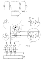
- a preferred embodiment of the detection device according to the invention comprises a matrix 1 of r x c, e.g. 10 x 10 radiation-sensitive pixel elements, on intervals of 100 um - complete dimension e.g. ⁇ 1 mm2 -, a trigger circuit 2 connected to each row r of radiation sensitive elements; a generator circuit 3 for generating column addresses; and analog amplifiers 4 for amplifying analog output signals when a radiation-sensitive pixel element is activated.
- the detection device 1 according to the present invention to be described below is fast, has a high position resolution, is easy to produce and is simple in design.
- the integrated circuit of Fig. 1 is preferably realised by a 3 um-p-well-CMOS process. As may be known to one skilled in the art, also other processes, which may for example provide different dimensions, can be used. High resistivity silicon is used for the application in which high energy particles are detected.
- diodes having a low potential should be avoided, also avoiding relatively deep wells in this region, as they collect charge.
- process steps are avoided in which high temperatures occur and in which a plasma is used, so as to maintain a long life cycle for minority carriers. As many etching steps as possible in the process are executed chemically.
- the drive-in step of the p-well (not shown) in which a higher temperature occurs during a substantial time period, is avoided by realising the p-well by means of ion implantation and a short annealing step.
- transistors and other elements using a p-channel on a high resistity substrate have a number of advantageous features, of which an important one relates to the fact that a displacement of the threshold voltage can be neglected when applying a bias voltage to the substrate, e.g. between 0 volts and a voltage at which the substrate is completely depleted.
- a diode D ij with a capacitance of 0,7 fF and an area of 100 x 100 (um)2 is located in the ith and jth row and shown in more detail below.
- the other, e.g. 99, diodes (not shown) are connected in the same manner as diode D ij .
- Fig. 2 an amount of charge is stored on the gate of a field effect transistor T1 if radiation R impinges on diode D ij connected to a supply voltage V b until such time as a shift register element 6, activated by a signal, supplies a columns signal C i to gates of transistors T2 and T3.
- transistor T1 and T2 are gated by column signal C i, transistor T1 is switched open, which controls a trigger element 8 from the trigger circuit 2 (Fig. 1).
- a current I1 controlled by charge present on the gate of FET T1 is supplied to a NOR circuit 7, to which also a signal ⁇ C i is supplied as a reading signal, delayed relative to signal C i .
- the signal coming from NOR gate 7 is inverted by invertor 9 and a trigger signal R j is therefore available, which indicates that in that particular row a diode D ij is activated.
- the signal R j is also fed back to the gate of a FET T5 whereby the charge present on the gate of the FET T1 can flow to an amplifying element 11 of the amplifier 4, and whereby the amplified signal E j is also available.
- the trigger element 8 is further provided with a FET T7 to the gate of which a signal r is to be applied, such that the trigger element 8 is reset to its starting position.
- Signal S applied to shift register element 6 may be the same as signal r.
- the column signal C i+1 derived from shift register element 6 ⁇ resets pixel element 1 through switching transistor T6.
- the degree of sensitivity to radiation of element D ij is set by adjusting the value V b as well as by adjusting the duration of the delay of signal ⁇ C1 relative to signal C1.
- the generator circuit 3 comprises, as shown in Fig. 2, a shift register made from elements 6; 6′ and 6 ⁇ with which the different columns of the pixel matrix 1 are consecutively controlled.
- a trigger signal R j ...R k is available at each row element of the column; at the same time the detected value of radiation is amplified to respective signals E j ...E k .
- At each column a radiation value is read out only of that pixel element to which radiation impinges, the other pixel elements not being read out because for those no trigger signal R j ...R k is produced. A substatial data reduction is thus achieved.
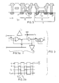
- FIG. 3a An embodiment of a shift register element 6 completely implemented in CMOS technology is shown in Fig. 3a, in which a shift signal S produces at time T1 the signal C i , after latch signal H has provided the possibility therefor of time T1.
- Signal r e acts as on reset signal.
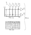
- Circuit 10 An output at X i of shift register element 6 is supplied to a circuit 10 shown in Fig. 4 for decoding from 2 n to N.
- Circuit 10 is a preferred embodiment integrated in a elegantly simple way.
- circuit 10 the encoding of a four bit signal (X i ,X i+1 ,X i+2 ,X i+3 ) to a two bit signal C* I , C* II is indicated by the table in Fig. 4b.
- the conversion takes place by means of a so-called GRAY code requiring only a minimal amount of energy (only one bit at a time is changed).
- the achievable frequency of the mentioned shifting operation and evaluation of the columns content is estimated to reach 20 MHz by an embodiment of the invention.
- the energy dissipation of an embodiment of the detection device according to the present invention of 50 x 50 pixel elements is 0.5 Watt at a frequency of 15 MHz and at a degree of activation of the rows of 90%.
- the detection device according to the present invention (Fig. 5) be realised in a n-Si substrate 14 by means of a CMOS-like structure having a p well 13 in which structure complementary field effect transistors 15, 16 respectively are disposed.
- the reading out electronics are to be spaced from the detector diodes at the mentioned bias voltage, so that no depleated region is formed therebetween. A lateral field is created by such a depleated region, whereby signal charge would be diverted.
- Only PMOS transistors are allowed in the high resistity substrate inside the detector region.
- the other circuits are disposed at a safe distance, e.g. the thickness of the Si chip (in the present case 400 ⁇ m).
- the threshold voltage of the p- and n-channel transistor is made approx. 0.5 V, e.g. by means of implantation (V T ).
Landscapes
- Physics & Mathematics (AREA)
- Health & Medical Sciences (AREA)
- Life Sciences & Earth Sciences (AREA)
- General Physics & Mathematics (AREA)
- High Energy & Nuclear Physics (AREA)
- Molecular Biology (AREA)
- Spectroscopy & Molecular Physics (AREA)
- Solid State Image Pick-Up Elements (AREA)
- Transforming Light Signals Into Electric Signals (AREA)
- Measurement Of Radiation (AREA)
Applications Claiming Priority (4)
| Application Number | Priority Date | Filing Date | Title |
|---|---|---|---|
| NL8801396 | 1988-05-31 | ||
| NL8801396 | 1988-05-31 | ||
| NL8802252A NL8802252A (nl) | 1988-05-31 | 1988-09-13 | Detectie-inrichting voor straling. |
| NL8802252 | 1988-09-13 |
Publications (2)
| Publication Number | Publication Date |
|---|---|
| EP0344866A2 true EP0344866A2 (de) | 1989-12-06 |
| EP0344866A3 EP0344866A3 (de) | 1990-09-05 |
Family
ID=26646386
Family Applications (1)
| Application Number | Title | Priority Date | Filing Date |
|---|---|---|---|
| EP19890201402 Ceased EP0344866A3 (de) | 1988-05-31 | 1989-05-31 | Detektionsvorrichtung für Strahlung |
Country Status (4)
| Country | Link |
|---|---|
| US (1) | US5023455A (de) |
| EP (1) | EP0344866A3 (de) |
| CA (1) | CA1310142C (de) |
| NL (1) | NL8802252A (de) |
Cited By (1)
| Publication number | Priority date | Publication date | Assignee | Title |
|---|---|---|---|---|
| US6153882A (en) * | 1997-07-04 | 2000-11-28 | Integrated Detector & Electronics As | Method and system for reading a data signal emitted by an active pixel in a sensor |
Families Citing this family (10)
| Publication number | Priority date | Publication date | Assignee | Title |
|---|---|---|---|---|
| JPH049706A (ja) * | 1990-04-27 | 1992-01-14 | Shimadzu Corp | 放射線像撮像装置 |
| US5235176A (en) * | 1992-07-30 | 1993-08-10 | General Electric Company | Optical radiation sensing assembly with increased resolution |
| US5336879A (en) * | 1993-05-28 | 1994-08-09 | David Sarnoff Research Center, Inc. | Pixel array having image forming pixel elements integral with peripheral circuit elements |
| US5325129A (en) * | 1993-06-07 | 1994-06-28 | Westinghouse Electric Corporation | Millimeter wavelength energy detector pixel having intermediate frequency amplification |
| IL123006A (en) | 1998-01-20 | 2005-12-18 | Edge Medical Devices Ltd | X-ray imaging system |
| IL126018A0 (en) | 1998-09-01 | 1999-05-09 | Edge Medical Devices Ltd | X-ray imaging system |
| AU5872099A (en) * | 1998-09-09 | 2000-03-27 | Oxford Instruments (Uk) Limited | Particle sensor |
| US6326625B1 (en) | 1999-01-20 | 2001-12-04 | Edge Medical Devices Ltd. | X-ray imaging system |
| US6178225B1 (en) | 1999-06-04 | 2001-01-23 | Edge Medical Devices Ltd. | System and method for management of X-ray imaging facilities |
| US20080203304A1 (en) * | 2007-02-22 | 2008-08-28 | The Regents Of The University Of Ca | Multichannel instrumentation for large detector arrays |
Family Cites Families (10)
| Publication number | Priority date | Publication date | Assignee | Title |
|---|---|---|---|---|
| US4176275A (en) * | 1977-08-22 | 1979-11-27 | Minnesota Mining And Manufacturing Company | Radiation imaging and readout system and method utilizing a multi-layered device having a photoconductive insulative layer |
| FR2469805A1 (fr) * | 1979-11-09 | 1981-05-22 | Thomson Csf | Matrice de detection d'un rayonnement electromagnetique et intensificateur d'images radiologiques comportant une telle matrice |
| FR2487566A1 (fr) * | 1980-07-25 | 1982-01-29 | Thomson Csf | Matrice de detection d'un rayonnement electromagnetique et intensificateur d'images radiologiques comportant une telle matrice |
| FR2517864A1 (fr) * | 1981-12-07 | 1983-06-10 | Telecommunications Sa | Dispositif d'enregistrement et de lecture d'images |
| JPS59108457A (ja) * | 1982-12-14 | 1984-06-22 | Olympus Optical Co Ltd | 固体撮像素子 |
| US4675739A (en) * | 1984-05-04 | 1987-06-23 | Energy Conversion Devices, Inc. | Integrated radiation sensing array |
| US4689487A (en) * | 1984-09-03 | 1987-08-25 | Kabushiki Kaisha Toshiba | Radiographic image detection apparatus |
| US4680471A (en) * | 1985-03-20 | 1987-07-14 | Motorola, Inc. | Integrated circuit packaging |
| DE3706252A1 (de) * | 1986-02-28 | 1987-09-03 | Canon Kk | Halbleiterfotosensor |
| JPS6312161A (ja) * | 1986-07-03 | 1988-01-19 | Olympus Optical Co Ltd | 半導体撮像装置 |
-
1988
- 1988-09-13 NL NL8802252A patent/NL8802252A/nl not_active Application Discontinuation
-
1989
- 1989-05-26 US US07/357,544 patent/US5023455A/en not_active Expired - Fee Related
- 1989-05-30 CA CA000601205A patent/CA1310142C/en not_active Expired - Lifetime
- 1989-05-31 EP EP19890201402 patent/EP0344866A3/de not_active Ceased
Cited By (1)
| Publication number | Priority date | Publication date | Assignee | Title |
|---|---|---|---|---|
| US6153882A (en) * | 1997-07-04 | 2000-11-28 | Integrated Detector & Electronics As | Method and system for reading a data signal emitted by an active pixel in a sensor |
Also Published As
| Publication number | Publication date |
|---|---|
| US5023455A (en) | 1991-06-11 |
| CA1310142C (en) | 1992-11-10 |
| NL8802252A (nl) | 1989-12-18 |
| EP0344866A3 (de) | 1990-09-05 |
Similar Documents
| Publication | Publication Date | Title |
|---|---|---|
| RU2339973C2 (ru) | Обнаружение заряда или частицы | |
| US6252462B1 (en) | Capacitor transimpedance amplifier ( CTIA) with shared load | |
| EP0344866A2 (de) | Detektionsvorrichtung für Strahlung | |
| US4659928A (en) | Focal plane array infrared device | |
| US6469740B1 (en) | Physical quantity distribution sensor and method for driving the same | |
| US3999082A (en) | Charge coupled amplifier | |
| US6121843A (en) | Charge mode capacitor transimpedance amplifier | |
| EP0493455A1 (de) | I.c. sensor. | |
| WO2003001567A2 (en) | High resolution, low power, wide dynamic range imager with embedded pixel processor and dram storage | |
| US4978872A (en) | Integrating capactively coupled transimpedance amplifier | |
| US4868902A (en) | GaAs capacitive feedback transimpedance amplifier | |
| EP0331695B1 (de) | Verstärker zur ablesung eines fotodetektors | |
| US20080180112A1 (en) | Numerical full well capacity extension for photo sensors with an integration capacitor in the readout circuit using two and four phase charge subtraction | |
| JP2001215152A (ja) | 赤外線固体撮像素子 | |
| US4109284A (en) | Self-scanning photo-sensitive circuits | |
| Plummer et al. | MOS electronics for a portable reading aid for the blind | |
| EP0377959B1 (de) | Verfahren zum Steuern einer Ladungsdetektorschaltung | |
| NL8901019A (nl) | Sensorschakeling voor gecorreleerde dubbele signaalbemonstering. | |
| US5039879A (en) | Digitally programmable gain normalization circuit | |
| US4775798A (en) | Device for detection with time delay and phase integration | |
| JPS6112408B2 (de) | ||
| US5172399A (en) | Semiconductor charge transfer device including charge quantity detection | |
| EP4272016B1 (de) | Festkörperstrahlungssensor zum erfassen von strahlungen, insbesondere teilchen, und verfahren zum erfassen von strahlungen, insbesondere teilchen | |
| KR100265139B1 (ko) | 광센서 수단에 빛이 조사되는 빈도를 감지하는 광센서 수단 | |
| US6528775B2 (en) | Charge-reading circuit protected against overloads coming from charges with undesirable polarity |
Legal Events
| Date | Code | Title | Description |
|---|---|---|---|
| PUAI | Public reference made under article 153(3) epc to a published international application that has entered the european phase |
Free format text: ORIGINAL CODE: 0009012 |
|
| AK | Designated contracting states |
Kind code of ref document: A2 Designated state(s): AT BE CH DE ES FR GB GR IT LI LU NL SE |
|
| PUAL | Search report despatched |
Free format text: ORIGINAL CODE: 0009013 |
|
| AK | Designated contracting states |
Kind code of ref document: A3 Designated state(s): AT BE CH DE ES FR GB GR IT LI LU NL SE |
|
| 17P | Request for examination filed |
Effective date: 19900917 |
|
| 17Q | First examination report despatched |
Effective date: 19930406 |
|
| STAA | Information on the status of an ep patent application or granted ep patent |
Free format text: STATUS: THE APPLICATION HAS BEEN REFUSED |
|
| 18R | Application refused |
Effective date: 19940603 |