EP0345773A2 - Mikroskop-Spektralgerät - Google Patents
Mikroskop-Spektralgerät Download PDFInfo
- Publication number
- EP0345773A2 EP0345773A2 EP89110378A EP89110378A EP0345773A2 EP 0345773 A2 EP0345773 A2 EP 0345773A2 EP 89110378 A EP89110378 A EP 89110378A EP 89110378 A EP89110378 A EP 89110378A EP 0345773 A2 EP0345773 A2 EP 0345773A2
- Authority
- EP
- European Patent Office
- Prior art keywords
- light
- spectrum
- microspectroscope
- illuminating light
- sample
- Prior art date
- Legal status (The legal status is an assumption and is not a legal conclusion. Google has not performed a legal analysis and makes no representation as to the accuracy of the status listed.)
- Granted
Links
- 238000001228 spectrum Methods 0.000 claims abstract description 106
- 230000003595 spectral effect Effects 0.000 claims abstract description 26
- 230000003287 optical effect Effects 0.000 claims description 83
- 230000002401 inhibitory effect Effects 0.000 claims description 8
- 238000003384 imaging method Methods 0.000 claims description 3
- 239000010408 film Substances 0.000 description 57
- 238000010586 diagram Methods 0.000 description 17
- 238000005259 measurement Methods 0.000 description 17
- 239000010409 thin film Substances 0.000 description 11
- 238000001514 detection method Methods 0.000 description 10
- 238000000034 method Methods 0.000 description 10
- 230000004044 response Effects 0.000 description 9
- 238000012544 monitoring process Methods 0.000 description 8
- 239000000758 substrate Substances 0.000 description 8
- 210000001747 pupil Anatomy 0.000 description 7
- 230000000694 effects Effects 0.000 description 6
- XUIMIQQOPSSXEZ-UHFFFAOYSA-N Silicon Chemical compound [Si] XUIMIQQOPSSXEZ-UHFFFAOYSA-N 0.000 description 2
- 230000009471 action Effects 0.000 description 2
- XAGFODPZIPBFFR-UHFFFAOYSA-N aluminium Chemical compound [Al] XAGFODPZIPBFFR-UHFFFAOYSA-N 0.000 description 2
- 229910052782 aluminium Inorganic materials 0.000 description 2
- 230000009467 reduction Effects 0.000 description 2
- 229910052710 silicon Inorganic materials 0.000 description 2
- 239000010703 silicon Substances 0.000 description 2
- 238000002834 transmittance Methods 0.000 description 2
- 241001417527 Pempheridae Species 0.000 description 1
- VYPSYNLAJGMNEJ-UHFFFAOYSA-N Silicium dioxide Chemical compound O=[Si]=O VYPSYNLAJGMNEJ-UHFFFAOYSA-N 0.000 description 1
- 230000005540 biological transmission Effects 0.000 description 1
- 230000008859 change Effects 0.000 description 1
- 230000021615 conjugation Effects 0.000 description 1
- 230000007613 environmental effect Effects 0.000 description 1
- 230000006870 function Effects 0.000 description 1
- 230000002452 interceptive effect Effects 0.000 description 1
- 239000000463 material Substances 0.000 description 1
- 230000002093 peripheral effect Effects 0.000 description 1
- 229910052814 silicon oxide Inorganic materials 0.000 description 1
Images


Classifications
-
- G—PHYSICS
- G01—MEASURING; TESTING
- G01N—INVESTIGATING OR ANALYSING MATERIALS BY DETERMINING THEIR CHEMICAL OR PHYSICAL PROPERTIES
- G01N21/00—Investigating or analysing materials by the use of optical means, i.e. using sub-millimetre waves, infrared, visible or ultraviolet light
- G01N21/17—Systems in which incident light is modified in accordance with the properties of the material investigated
- G01N21/25—Colour; Spectral properties, i.e. comparison of effect of material on the light at two or more different wavelengths or wavelength bands
- G01N21/27—Colour; Spectral properties, i.e. comparison of effect of material on the light at two or more different wavelengths or wavelength bands using photo-electric detection ; circuits for computing concentration
- G01N21/274—Calibration, base line adjustment, drift correction
-
- G—PHYSICS
- G01—MEASURING; TESTING
- G01B—MEASURING LENGTH, THICKNESS OR SIMILAR LINEAR DIMENSIONS; MEASURING ANGLES; MEASURING AREAS; MEASURING IRREGULARITIES OF SURFACES OR CONTOURS
- G01B11/00—Measuring arrangements characterised by the use of optical techniques
- G01B11/02—Measuring arrangements characterised by the use of optical techniques for measuring length, width or thickness
- G01B11/06—Measuring arrangements characterised by the use of optical techniques for measuring length, width or thickness for measuring thickness ; e.g. of sheet material
-
- G—PHYSICS
- G01—MEASURING; TESTING
- G01J—MEASUREMENT OF INTENSITY, VELOCITY, SPECTRAL CONTENT, POLARISATION, PHASE OR PULSE CHARACTERISTICS OF INFRARED, VISIBLE OR ULTRAVIOLET LIGHT; COLORIMETRY; RADIATION PYROMETRY
- G01J3/00—Spectrometry; Spectrophotometry; Monochromators; Measuring colours
- G01J3/28—Investigating the spectrum
- G01J3/42—Absorption spectrometry; Double beam spectrometry; Flicker spectrometry; Reflection spectrometry
- G01J2003/425—Reflectance
-
- G—PHYSICS
- G01—MEASURING; TESTING
- G01J—MEASUREMENT OF INTENSITY, VELOCITY, SPECTRAL CONTENT, POLARISATION, PHASE OR PULSE CHARACTERISTICS OF INFRARED, VISIBLE OR ULTRAVIOLET LIGHT; COLORIMETRY; RADIATION PYROMETRY
- G01J3/00—Spectrometry; Spectrophotometry; Monochromators; Measuring colours
- G01J3/28—Investigating the spectrum
- G01J3/2823—Imaging spectrometer
-
- G—PHYSICS
- G01—MEASURING; TESTING
- G01N—INVESTIGATING OR ANALYSING MATERIALS BY DETERMINING THEIR CHEMICAL OR PHYSICAL PROPERTIES
- G01N2201/00—Features of devices classified in G01N21/00
- G01N2201/12—Circuits of general importance; Signal processing
- G01N2201/127—Calibration; base line adjustment; drift compensation
- G01N2201/12746—Calibration values determination
- G01N2201/12753—Calibration values determination and storage
Definitions
- the present invention relates to a microspectroscope for detecting the spectrum of observed light outgoing from a sample to be measured.
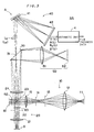
- Fig. 1 is a schematic block diagram showing a conventional microspectroscope 1.
- the microspectroscope 1 comprises an illuminating optical system 10, a microscopic optical system 20, a reflecting mirror 30, a spectroscopic unit 40, and a monitoring optical system 50.
- the illuminating optical system 10 is formed by a light source 11, a condenser lens 12, an aperture stop 13, a field stop 14 and another condenser lens 15, so that illuminating light outgoing from the light source 11 is guided to the microscopic optical system 20 through the condenser lens 12, the aperture stop 13, the field stop 14 and the condenser lens 15.
- the microscopic optical system 20 is formed by an objective lens 21, an image-formation lens 24 and a beam splitter 23 provided between the objective lens 21 and the image-formation lens 24.
- Symbol 22 denotes a pupil position of the objective lens 21.
- the illuminating light outgoing from the light source 11 passes through the condenser lens 12, the aperture stop 13, the field stop 14 and the condenser lens 15, and is guided to the objective lens 21 by the beam splitter 23.
- the illuminating light transmitted through the objective lens 21 is applied onto the surface of a sample S which is supported by a sample holder (not shown).
- Reflected light reflected by the surface of the sample 5 is enlarged and imaged in a position close to the reflecting mirror 30 through the objective lens 21, the beam splitter 23 and the image-formation lens 24.
- the reflecting mirror 30 is provided with a pinhole 31. Within the reflected light, therefore, reflected light L S passing through the pinhole 31 is taken in the spectroscopic unit 40.
- the spectroscopic unit 40 is formed by a diffraction grating 41 for separating the reflected light L S into spectral components and a photo detector 42 for detecting the spectrum of the light spectrally diffracted by the diffraction grating 41.
- the diffraction grating 41 may be prepared by a flat field type diffraction grating which images a spectrum on a flat plane, for example. Alternatively, the diffraction grating may be prepared by that having a sweeper.
- the photo detector 42 which is formed by a photodiode array or a CCD, for example, is conjugated with the pinhole 31. Alternatively, the photo detector 42 may be prepared by a photomultiplier.
- the spectroscopic unit 40 Since the spectroscopic unit 40 has the aforementioned structure, the reflected light L S taken in the spectroscopic unit 40 is separated into its spectral components by the diffraction grating 41, and the respective spectral components of the light L S are received by the photo detector 42, which in turn outputs a signal corresponding to the spectrum of the light L S .
- a sample S which comprises a substrate and a transparent thin film formed thereon, such as a silicon substrate and a silicon oxide film
- a transparent thin film formed thereon such as a silicon substrate and a silicon oxide film
- light reflected by the surface of the thin film and that transmitted through the thin film and then reflected by the surface of the substrate are taken in the microspectroscope while interfering with each other.
- the degree of such interference depends on the indexes of refraction of the substrate and the thin film, the thickness of the thin film and the wavelength of the illuminating light.
- the conventional microspectroscope 1 is generally applied to a film thickness measuring apparatus.
- such a film thickness measuring apparatus 2 is formed by the microspectroscope 1 and an arithmetic unit 3, so that the microspectroscope 1 detects the spectrum of the sample S and the arithmetic unit 3 operates the film thickness of the sample S on the basis of spectral data obtained by the microspectroscope 1.
- the spectrum detected by the microspectroscope 1 is influenced by various factors such as spectral transmittance characteristics of the illuminating optical system 10 and the microscopic optical system 20, luminous energy loss caused when the light passes through these optical systems, the spectral characteristic of the diffraction grating 41, the spectral-response characteristic of the photo detector 42, and the like. In order to accurately measure the film thickness of the sample S, it is necessary to eliminate such influences.
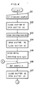
- Fig. 2 is a flow chart showing a method of measuring film thickness by the film thickness measuring apparatus 2.
- an operator previously inputs spectrum data B( ⁇ ) of a sample (hereinafter referred to as "standard sample"), whose spectrum data is family to, in the arithmetic unit 3 through a keyboard (not shown), to store the data in a memory (not shown) provided in the arithmetic unit 3.
- the standard sample may be prepared by a silicon substrate, a substrate which is deposited with aluminum on its surface, or the like.
- the operator sets the standard sample on the sample holder of the microspectroscope 1 (step S1), and supplies a command outputted for detecting calibration data to the arithmetic unit 3.
- the microspectroscpe 1 detects the spectrum of the standard sample, to store data B′( ⁇ ) relating to the spectrum in the memory of the arithmetic unit 3 (step S2).
- the operator takes out the standard sample from the sample holder of the microspectroscope 1 and sets the sample S on the sample holder of the microspectroscope 1 (step S3). Thereafter the operator supplies a command for starting measurement to the arithmetic unit 3, so that the microspectroscope 1 detects the spectrum of the sample S in response to a command outputted from the arithmetic unit 3, to store data S′( ⁇ ) relating to the spectrum thereof in the memory of the arithmetic unit 3 (step S4).
- step S5 the data S′( ⁇ ), B( ⁇ ), and B′( ⁇ ) stored in the memory are read in the arithmetic unit 3, to obtain data S( ⁇ ) in accordance with the following expression:
- the data S( ⁇ ) corresponds to a signal outputted from the microspectroscope 1 on the assumption that absolutely no influence is caused by the aforementioned factors. In other words, the data S( ⁇ ) shows the true spectrum of the sample S.
- the arithmetic unit 3 operates the thickness of the thin film (step S6).
- the principle of operating film thickness is well known in the art, and hence description thereof is omitted.
- the data S′( ⁇ ) relating to the actually measured spectrum is calibrated in the aforementioned manner to obtain the data S( ⁇ ) relating to the true spectrum, whereby the film thickness can be accurately measured.
- the steps S3 to S6 are repeated in order to measure the thickness of a subsequent sample S, to thereby continuously accurately measure the film thickness.
- the spectrum is also influenced by factors other than the above, such as spectral emissivity which is changed following change in ambient temperature of the light source 11, for example.
- spectral emissivity is also changed in response, to vary the spectrum acturally measured by the microspectroscope 1.
- first characteristic spectral emissivity characteristic
- the present invention is directed to a microspectroscope which actually measures spectra B′( ⁇ ) and S′( ⁇ ) of a standard sample whose spectrum B( ⁇ ) is known and an objective sample, to correct the spectrum S′( ⁇ ) on the basis of the spectrum B′( ⁇ ).
- the microspectroscope comprises: (a) a sample holder for holding the standard sample and the objective sample; (b) a light source for projecting illuminating light toward the sample holder; (c) a microscopic optical system for imaging observed light outgoing from the sample held in said sample holder in a prescribed imaging position; (d) first spectroscopic means for taking in the observed light through the microscopic optical system for separating the observed light into spectral components; (e) first detector means for detecting the spectrum of the observed light separated into spectral components by the first sepctroscopic means; (f) second spectroscopic means for separating the illuminating light into spectral components; (g) second detector means for detecting the spectrum of the illuminating light separated into spectral components by the second specroscopic means; (h) a memory for storing data relating to the spectra outputted from the first and second detector means; and (i) calibration means comprising (i-1) first means for measuring the spectrum B′
- the spectrum B′( ⁇ ) of the observed light outgoing from the standard sample whose spectrum B( ⁇ ) is known is detected while the spectrum R0( ⁇ ) of the illuminating is detected.
- the spectrum S′( ⁇ ) of the observed light outgoing from the objective sample is detected while the spectrum R( ⁇ ) of the illuminating light is detected.
- the spectrum S′( ⁇ ) is corrected on the basis of the spectra B( ⁇ ), B′( ⁇ ), R0( ⁇ ) and R( ⁇ ), to thereby prevent reduction in detecetion accuracy caused by variation in ambient temperature of the apparatus, humidity or the like.
- the first spectroscopic means also serves as the second spectroscopic means while the first detector means also serves as the second detector means
- the apparatus further comprises optical means for guiding the illuminating light from the light source to the first spectroscopic means while inhibiting from projecting the illuminating light toward the sample holder in detection of the spectrum of the illuminating light, while guiding the illuminating toward the surface of the sample holder in detection of the spectrum of the observed light.
- the first spectroscopic means also serves as the second spectroscopic means while the microscopic optical system includes a beam splitter for overlapping the illuminating light outgoing from the light source with an optical path of the observed light
- the apparatus further comprises reflecting means for reflecting illuminating light transmitted through the beam splitter toward the beam splitter, first optical means provided between the sample holder and the beam splitter for inhibiting passage of light guided to the second detector means within the observed light, and second optical means provided between the reflecting means and the beam splitter for inhibiting passage of light guided to the first detector means within the light outgoing from the reflecting means.
- the microspectroscope further comprises arithmetic means for obtaining film thickness of the objective sample on the basis of data obtained by correcting the data S′( ⁇ ) by the calibration means.
- a principal object of the present invention is to provide a microspectroscope which can more easily prevent reduction in detection accuracy caused by variation in ambient temperature of the apparatus, humidity and the like.
- Another object of the present invention is to provide a microspectroscope which is simple in detection procedure, in addition to the aforementioned object.
- Fig. 3 is a schematic block diagram showing a microspectroscope A according to a first embodiment of the present invention.
- the microspectroscope A is formed by an illuminating optical system 10, a microscopic optical system 20, a reflecting mirror 30, a spectroscopic unit 40, a monitoring optical system 50, another reflecting mirror 61, and shutters 62 and 63.
- the illuminating optical system 10, the microscopic optical system 20, the reflecting mirror 30, the spectroscopic unit 40 and the monitoring optical system 50 are identical to those in the prior art shown in Fig. 1, and hence redundant description is omitted.
- the reflecting mirror 61 is provided on an optical path of illuminating light outgoing from a light source 11 in a position symmetrical with a pupil position 22 with respect to a beam splitter 23.
- the position of the reflecting mirror 61 is not restricted to this but may be slightly moved on the optical path of the illuminating light, as a matter of course.
- the reflecting mirror 61 desirably has substantially uniform spectral reflectance within a wavelength range for spectral diffraction, and is prepared by a mirror deposited with aluminum etc., whose spectral reflectance is not extremely changed within the said range.
- the shutter 62 is arranged between the reflecting mirror 61 and the beam splitter 23, while the other shutter 63 is arranged between the pupil position 22 of an objective lens 21 and the beam splitter 23.
- the shutters 62 and 63 are opened and closed by commands outputted from an arithmetic unit 4.
- the shutter 63 is not restricted to the position between the pupil position 22 and the beam splitter 23, but may be appropriately located between a sample S and the beam splitter 23.
- the aforementioned microspectroscope A can be applied to a film thickness measuring apparatus, similarly to the prior art.
- Symbol AA in Fig. 3 denotes a film thickness measuring apparatus.
- the film thickness measuring apparatus AA is formed by the microspectroscope A and the arithmetic unit 4, which operates film thickness in accordance with the following procedure while controlling the microspectroscope A:
- Fig. 4 is a flow chart showing a method of measuring film thickness by the film thickness measuring apparatus AA.
- an operator inputs data B( ⁇ ) relating to a known spectrum of a standard sample in the arithmetic unit 4 through a keyboard (not shown), to store the same in a memory (not shown) provided in the arithmetic unit 4.
- the operator further previously operates data (hereinaftre referred to as "reference data”) relating to the spectrum with respect to thickness of a thin film on the basis of indexes of reflection of a substrate and the thin film of the sample S every constant thickness space and inputs the result of operation in the arithmetic unit 4 through the keyboard, to store the same in the memory of the arithmetic unit 4.
- reference data data relating to the spectrum with respect to thickness of a thin film on the basis of indexes of reflection of a substrate and the thin film of the sample S every constant thickness space and inputs the result of operation in the arithmetic unit 4 through the keyboard, to store the same in the memory of the arithmetic unit 4.
- the operator sets the standard sample in a sample holder (step S11) and supplies a command for detecting calibration data to the arithmetic unit 4.
- the shutters 62 and 63 are set in a closed state and an opened state respectively (step S12), so that illuminating light outgoing from the light source 11 is applied to the surface of the standard sample when the light source 11 is turned on. Observed light reflected by the surface of the standard sample is enlarged and imaged in a position close to the reflecting mirror 30 through the objective lens 21 and an image-formation lens 24.
- observed light L S passing through a pinhole 31 is taken in the spectroscopic unit 40, which in turn detects the spectrum of the observed light L S . Further, data B′( ⁇ ) relating to the spectrum is supplied from a photo detector 42 to the arithmetic unit 4, and stored in the memory (step S13).
- the shutters 62 and 63 are again set in an opened state and a closed state, respectively, in response to commands outputted from the arithmetic unit 4 (step S14).
- the light source 11 is turned on and illuminating light is applied to the reflecting mirror 61 through a condenser lens 12, an aperture stop 13, a field stop 14, another condenser lens 15, the beam splitter 23 and the shutter 62.
- Reflected light reflected by the reflecting mirror 61 is guided toward the image-formation lens 24 by the beam splitter 23, to be enlarged and image in a position close to the reflecting mirror 30 through the image-formation lens 24.
- reflected light L R passing through the pinhole 31 is taken in the spectroscopic unit 40, and the photo detector 42 detects the spectrum of the reflected light L R . Further, data R0( ⁇ ) relating to the spectrum is supplied from the photo detector 42 to the arithmetic unit 4, to be stored in the memory (step S15).
- the data R0( ⁇ ) shows spectral emissivity of the light source 11 in measurement of the spectral data B′( ⁇ ).
- step S16 the operator takes out the standard sample from the sample holder and sets the sample S in the sample holder (step S16). Then the operator supplies a command for starting measurement to the arithmetic unit 4, whereby the microspectroscope A is controlled in response to a command outputted from the arithmetic unit 4, to correctly obtain film thickness of the sample S as follows:
- the shutters 62 and 63 are set in a closed state and an opened state, respectively (step S17) so that the spectrum of observed light L S is detected similarly to the above, and data S′( ⁇ ) relating to the spectrum of the observed light L S is stored in the memory provided in the arithmetic unit 4 (step S18).
- step S18 the shutters 62 and 63 are again set in an opened state and a closed state, respectively (step S19), so that the spectrum of the reflected light L R is detected similarly to the above and data R( ⁇ ) relating to the spectrum of the reflected light L R is stored in the memory of the arithmetic unit 4 (step S20).
- the light source 11 has a second characteristic in measurement of the data S′( ⁇ ) (step S18) while the same has a first characteristic in measurement of the data B′( ⁇ ) (step S13), the data S( ⁇ ) relating to the spectrum of the sample S can be correctly detected since the amount of variation in spectral emissivity of the light source 11 is corrected on the basis of the data R0( ⁇ ) and R( ⁇ ).
- step S22 Thereafter the data S( ⁇ ) is compared with reference data stored in the memory, so that the film thickness of the sample S is obtained.
- the data S′( ⁇ ) relating to the actually measured spectrum is calibrated in the aforementioned manner to obtain the film thickness on the basis of the calibrated data S( ⁇ ) whereby accuracy in measurement of the film thickness can be improved.
- errors caused by variation in spectral emissivity of the light source 11 can be calibrated by only switching closed and opened states of the shutters 62 and 63, to thereby improve operation efficiency.
- the data R( ⁇ ) is detected immediately after detection of the data S′( ⁇ ), the same may be detected immediately before detection of the data S′( ⁇ ).
- the method of obtaining film thickness on the basis of the data S( ⁇ ) is not restricted to the above but a well-known method such as that disclosed in Japanese Patent Laying-Open Gazette No. 217705/1986 is also applicable.
- Fig. 5 is a block diagram showing an essential part of a microspectroscope according to a second embodiment of the present invention.
- An illuminating optical system 10, a microscopic optical system 20, an objective lens 71, a reflecting mirror 72 and shutters 73 and 74, which are components of a microspectroscope B, are shown in Fig. 5.
- Other components reflecting mirror 30, spectroscopic unit 40 and monitoring optical system 50
- Numeral 75 denotes a pupil position of the objective lens 71.
- the objective lens 71 which is substantially identical in spectral transmittance and aperture number to an objective lens 21, is located symmetrically to the objective lens 21 of the microscopic optical system 20 with respect to a beam splitter 23.
- the reflecting mirror 72 is provided in a front focal position of the objective lens 71.
- the shutters 73 and 74 are arranged between the beam splitter 23 and the pupil positions 75 and 22, respectively.
- the microspectroscope B can be applied to a film thickness measuring apparatus.
- a film thickness measuring apparatus is identical in structure to the film thickness measuring apparatus AA shown in Fig. 3 except for that the objective lens 71 is provided, and its operation is also identical to that of the apparatus AA (Fig. 4). According to the second embodiment, therefore, an effect identical to that of the first embodiment can be attained.
- optical condition between the reflecting mirror 72 and the beam splitter 23 is substantially identical to that between a sample S and the beam splitter 23.
- Fig. 6 is a flow chart showing the operation of a film thickness measuring apparatus, in which the reflecting mirror 72 is formed by a standard sample. Similarly to the first embodiment, the operator stores data B( ⁇ ) relating to the spectrum of the standard sample and previously operated reference data in the memory, respectively, in advance of film thickness measurement.
- step S16 the operator sets the sample S in a sample holder (step S16) and thereafter supplies a command for starting measurement to an arithmetic unit 4 so that the entire apparatus is controlled in response to a command outputted from the arithmetic unit 4, to thereby correctly obtain the film thickness of the sample S in the following manner:
- the shutters 73 and 74 are set in a closed state and an opened state, respectively (step S17′), so that the spectrum of observed light is detected similarly to the above and data S′( ⁇ ) relating to the spectrum of the observed light is stored in the memory (step S18).
- step S19′ the shutters 73 and 74 are set in an opened state and a closed state, respectively (step S19′), and the spectrum of reflected light reflected by the reflecting mirror 72 is detected similarly to the above, so that data B ⁇ ( ⁇ ) relating to the spectrum of the reflected light is stored in the memory (step S20′).
- step S21 There is no need to consider an error caused by variation in spectral emissivity of a light source 11, since the data B ⁇ ( ⁇ ) is detected immediately after detection of the data S′( ⁇ ).
- step S22 Thereafter the data S( ⁇ ) is compared with the reference data stored in the memory, to obtain the film thickness of the sample S (step S22).
- Film thickness can be continuously measured by repeating the steps S16 to S22 in particular.
- the measurement procedure is extremely simplified when the reflecting mirror 72 is formed by a standard sample, to further improve operation efficiency.
- Fig. 7 is a block diagram showing an essential part of a microspectroscope according to a third embodiment of the present invention.
- This microspectroscope C has a reflecting mirror 81 provided between a beam splitter 23 and a pupil position 22 in place of the reflecting mirror 61 and the shutters 62 and 63 of the first embodiment.
- the reflecting mirror 81 is adapted to reciprocate along an X-axis by driving means (not shown).
- Other structure of this embodiment is identical to that of the microspectroscope A.
- this microspectroscope C can be applied to a film thickness measuring apparatus.
- the film thickness measuring apparatus to which the microspectroscope C is applied is identical in operation to the apparatus AA except for the following two points: While the shutters 62 and 63 are set in an opened state and a closed state at the steps S14 and S19 in the film thickness measuring apparatus AA, the reflecting mirror 81 is located on an image-formation optical axis in the film thickness measuring apparatus to which the microspectroscope C is applied, as shown in Fig. 7. Further, while the shutters 62 and 63 are set in a closed state and an opened state respectively at the steps S12 and S17, the reflecting mirror 81 is moved to be evacuated from the image-formation optical path in the film thickness measuring apparatus to which the microspectroscope C is applied.
- Fig. 8 is a block diagram showing an essential part of a microspectroscope according to a fourth embodiment of the present invention.
- the microspectroscope D is provided with reflecting mirrors 91, 92 and 94 and lenses 93, 95 and 96 in place of the reflecting mirror 61 and the shutters 62 and 63 of the first embodiment.
- the reflecting mirrors 91 and 92 are provided in an illuminating optical system 10 and a microscopic optical system 20, respectively, and are adapted to be synchronously reciprocated in a direction perpendicular to the plane of the figure by driving means (not shown).
- Other structure of this embodiment is identical to that of the microspectroscope A.
- the microspectroscope D can be applied to a film thickness measuring apparatus.
- the film thickness measuring apparatus to which the microspectroscope D is applied is identical in operation to the apparatus AA, except for the following two points: While the shutters 62 and 63 are set in an opened state and a closed state respectively at the steps S14 and S19 in the film thickness measuring apparatus AA, the reflecting mirrors 91 and 92 are located on an illuminating optical path and an image-formation optical path respectively in the film thickness measuring apparatus to which the microspectroscope D is applied, as shown in Fig. 8.
- illuminating light outgoing from a light source 11 is not applied to the surface of a sample S, but guided to an image-formation position side of the microscopic optical system 20 through the reflecting mirror 91, the lens 93, the reflecting mirror 94, the lenses 95 and 96 and the reflecting mirror 92.
- the shutters 62 and 63 are set in a closed state and an opened state respectively at the steps S12 and S17 in the film thickness measuring apparatus AA, the reflecting mirrors 91 and 92 are moved to be evacuated from the illuminating optical path and the image-formation optical path respectively in the film thickness measuring apparatus to which the microspectrosope D is applied.
- Fig. 9A is a perspective view showing an essential part of a microspectroscope according to a fifth embodiment of the present invention
- Fig. 9B is a block diagram showing another essential part of the fifth embodiment.
- Fig. 9A shows a reflecting mirror 30′ and a spectroscopic unit 40′ which are components of a microspectroscope E.
- Fig. 9B shows a beam splitter 23, a relay lens 103, a lens 104, a reflecting mirror 105 and a filter 106 which are also components of the microspectroscope E.
- Other components (illuminating optical system 10, microscopic optical system 20, monitoring optical system 50 and arithmetic unit 4) are identical to those of the first to fourth embodiments, and omitted from the figures.
- the reflecting mirror 30′ is provided with a pinhole 32 for taking only observed light in the spectroscopic unit 40′ and another pinhole 33 for taking only reflected light in the same with a prescribed space interval.
- photo detectors 101 and 102 are provided in conjugation with the pinholes 33 and 32, respectively.
- the illuminating light transmitted through the beam splitter 23 is applied to the reflecting mirror 105 through the relay lens 103 and the objective lens 104.
- the relay lens 103 is provided with a filter 106, which has a shielding region 107 (Fig. 9C) in a position corresponding to the pinhole 32 for the observed light. Within reflected light reflected by the reflecting mirror 105, therefore, light corresponding to the shielding region 107 is not applied to the pinhole 32.
- Another lens (not shown) equivalent to the relay lens 103 is also provided between the beam splitter 23 and the objective lens 21.
- This lens is provided with a filter having a shielding region in a position corresponding to the pinhole 33 for the reflected light. Within the observed light reflected by a sample S, therefore, light corresponding to the shielding region is not applied to the pinhole 33.
- a light source 11 When a light source 11 is turned on, illuminating light outgoing from the light source 11 is applied to the reflecting mirror 105 through the beam splitter 23, the relay lens 103 and the objective lens 104. Reflected light reflected by the reflecting mirror 105 is guided toward an image-formation lens 24 by the beam splitter 23, to be enlarged and imaged in a position close to the reflecting mirror 30′ through the image-formation lens 24. However, the reflected light is not applied to the pinhole 32 through action of the shielding region 107 of the filter 106.
- the illuminating light is also applied to the surface of the sample S, so that the observed light reflected by the surface of the sample S is enlarged and imaged in a position close to the reflecting mirror 30′ through the beam splitter 23 and the image-formation lens 24.
- the observed light is not applied to the pinhole 33 through action of the shielding region of the filter, similarly to the aforementioned reflected light.
- the spectra of the reflected light L R and the observed light L S can be simultaneously detected according to this embodiment, whereby the detection procedure can be further simplified as compared with the first to fourth embodiments.
- data R( ⁇ ) relating to the spectrum of the reflected light L R and data S′( ⁇ ) relating to the spectrum of the observed light L S may not be stored in a memory. Since the data R( ⁇ ) and S′( ⁇ ) are simultaneously detected, the true data S( ⁇ ) can be obtained without the data S′( ⁇ ) and R( ⁇ ) storing by the following means: When the data R( ⁇ ) and S′( ⁇ ) are detected, the ratio of the data S′( ⁇ ) to R( ⁇ ) are obtained through hardware having an appropriate arithmetic circuit. Thereafter, the arithmetic unit 4 reads data R0( ⁇ ) stored in the memory, to thereby obtain the data S( ⁇ ) by multiplying the same by the said ratio.
- Fig. 10 is a block diagram showing an essential part of a microspectroscope according to a sixth embodiment of the present invention. As shown in Fig. 10, this microspectroscope F is provided with a spectroscopic unit 110 on an illuminating optical path. Other components (illuminating optical system 10, microscopic optical system 20, reflecting mirror 30, spectroscopic unit 40 and monitoring optical system 50) are identical to those of the aforementioned embodiments, and omitted from the figure.
- the spectroscopic unit 110 is formed by optical filters 111a, 111b and 111c provided on the optical path of illuminating light for reflecting only light components of prescribed wavelengths and photo detectors 112a, 112b, 112c and 112d such as photodiodes provided in correspondence to the optical filters 111a, 111b and 111c, respectively.
- the number of the optical filters 111a, 111b and 111c is not restricted to three but may be appropriately decided in response to characteristics of a light source 11, accuracy of measurement etc.
- the illuminating light outgoing from the light source 11 is taken in the spectroscopic unit 110 and the spectrum of the illuminating light is detected by the photo detectors 112a, 112b and 112c, while observed light L S is taken in the spectroscopic unit 40 and the spectrum of the observed light L S is detected by a photo detector 42 at the same time, similarly to the prior art.
- Fig. 11 is a block diagram showing an essential part of a microspectroscope according to a seventh embodiment of the present invention. Similarly to the sixth embodiment, this microspectroscope G is provided with a spectroscopic unit 120 on an illuminating optical path.
- the spectroscopic unit 120 is formed by a prism 121 provided on the optical path of illuminating light and a photo detector 122 such as a CCD for detecting the spectrum obtained through the prism 121.
- illuminating light outgoing from the light source 11 is taken in the spectroscopic unit 120 and the spectrum of the illuminating light is detected similarly to the sixth embodiment, while observed light L S is taken in a spectroscopic unit 40 and the spectrum of the observed light L S is detected by a photo detector 42 at the same time, similarly to the prior art.
- the present invention is not restricted to the aforementioned embodiments, but the first embodiment (Fig. 3) may be replaced structure formed by the illuminating optical system 10 of the first embodiment and another structure formed by a microscopic optical system 20, a reflecting mirror 30, a spectroscopic unit 40 and a monitoring optical system 50 each other, as shown in Fig. 12, for example.
- diffraction grating 41 is employed as spetroscopic means of the spectroscopic unit 40 or 40′ in each of the first to fifth embodiments, an optical element having a spectroscopic function, such as a prism, can be alternatively employed.
- microspectroscope is applied to a film thickness measuring apparatus in each of the aforementioned embodiments, the present invention is not restricted to such a film thickness measuring apparatus.
Landscapes
- Physics & Mathematics (AREA)
- Spectroscopy & Molecular Physics (AREA)
- General Physics & Mathematics (AREA)
- Analytical Chemistry (AREA)
- General Health & Medical Sciences (AREA)
- Health & Medical Sciences (AREA)
- Life Sciences & Earth Sciences (AREA)
- Chemical & Material Sciences (AREA)
- Mathematical Physics (AREA)
- Biochemistry (AREA)
- Theoretical Computer Science (AREA)
- Engineering & Computer Science (AREA)
- Immunology (AREA)
- Pathology (AREA)
- Length Measuring Devices By Optical Means (AREA)
- Investigating Or Analysing Materials By Optical Means (AREA)
- Spectrometry And Color Measurement (AREA)
- Microscoopes, Condenser (AREA)
Applications Claiming Priority (2)
| Application Number | Priority Date | Filing Date | Title |
|---|---|---|---|
| JP63140733A JPH073365B2 (ja) | 1988-06-08 | 1988-06-08 | 顕微分光装置 |
| JP140733/88 | 1988-06-08 |
Publications (3)
| Publication Number | Publication Date |
|---|---|
| EP0345773A2 true EP0345773A2 (de) | 1989-12-13 |
| EP0345773A3 EP0345773A3 (de) | 1991-04-24 |
| EP0345773B1 EP0345773B1 (de) | 1995-02-22 |
Family
ID=15275442
Family Applications (1)
| Application Number | Title | Priority Date | Filing Date |
|---|---|---|---|
| EP89110378A Expired - Lifetime EP0345773B1 (de) | 1988-06-08 | 1989-06-08 | Mikroskop-Spektralgerät |
Country Status (4)
| Country | Link |
|---|---|
| US (1) | US5048960A (de) |
| EP (1) | EP0345773B1 (de) |
| JP (1) | JPH073365B2 (de) |
| DE (1) | DE68921249T2 (de) |
Cited By (5)
| Publication number | Priority date | Publication date | Assignee | Title |
|---|---|---|---|---|
| EP0538664A3 (en) * | 1991-10-05 | 1993-07-14 | Ultrakust Electronic Gmbh | Method and device for determining optical spectral shifts caused by physical or chemical effects |
| WO1997024605A1 (de) * | 1995-12-27 | 1997-07-10 | Bran + Luebbe Gmbh | Verfahren und gerätekombination zur herstellung der vergleichbarkeit von spektrometermessungen |
| WO1997031239A1 (en) * | 1996-02-20 | 1997-08-28 | National Research Council Of Canada | A method and apparatus for reducing the unwanted effects of noise present in a three-dimensional color imaging system |
| US6222187B1 (en) * | 1997-07-03 | 2001-04-24 | Institute Of Microelectronics | Multiwavelength imaging and spectroscopic photoemission microscope system |
| CN103954361A (zh) * | 2014-04-29 | 2014-07-30 | 中国科学院光电研究院 | 一种大孔径多通道空间外差干涉光谱成像方法及光谱仪 |
Families Citing this family (18)
| Publication number | Priority date | Publication date | Assignee | Title |
|---|---|---|---|---|
| US5166080A (en) * | 1991-04-29 | 1992-11-24 | Luxtron Corporation | Techniques for measuring the thickness of a film formed on a substrate |
| US5310260A (en) * | 1990-04-10 | 1994-05-10 | Luxtron Corporation | Non-contact optical techniques for measuring surface conditions |
| US5154512A (en) * | 1990-04-10 | 1992-10-13 | Luxtron Corporation | Non-contact techniques for measuring temperature or radiation-heated objects |
| US5769540A (en) * | 1990-04-10 | 1998-06-23 | Luxtron Corporation | Non-contact optical techniques for measuring surface conditions |
| JP2699753B2 (ja) * | 1992-02-28 | 1998-01-19 | 株式会社島津製作所 | 分光光度計 |
| US5747813A (en) * | 1992-06-16 | 1998-05-05 | Kla-Tencop. Corporation | Broadband microspectro-reflectometer |
| US5486701A (en) * | 1992-06-16 | 1996-01-23 | Prometrix Corporation | Method and apparatus for measuring reflectance in two wavelength bands to enable determination of thin film thickness |
| US5371586A (en) * | 1992-10-09 | 1994-12-06 | Instruments Sa, Inc. | Low aberration diffraction grating system |
| US20070299808A1 (en) * | 1995-05-19 | 2007-12-27 | Cyberfone Technologies, Inc. | Telephone/Transaction Entry Device and System for Entering Transaction Data into Databases |
| JP2853615B2 (ja) * | 1995-08-09 | 1999-02-03 | 富士ゼロックス株式会社 | 電子写真感光体の評価装置および評価方法、電子写真感光体の製造装置および製造方法 |
| JP2004505273A (ja) | 2000-08-01 | 2004-02-19 | ボード・オブ・リージエンツ,ザ・ユニバーシテイ・オブ・テキサス・システム | 転写リソグラフィのための透明テンプレートと基板の間のギャップおよび配向を高精度でセンシングするための方法 |
| US6633391B1 (en) | 2000-11-07 | 2003-10-14 | Applied Materials, Inc | Monitoring of film characteristics during plasma-based semi-conductor processing using optical emission spectroscopy |
| US6603538B1 (en) | 2000-11-21 | 2003-08-05 | Applied Materials, Inc. | Method and apparatus employing optical emission spectroscopy to detect a fault in process conditions of a semiconductor processing system |
| US6917421B1 (en) * | 2001-10-12 | 2005-07-12 | Kla-Tencor Technologies Corp. | Systems and methods for multi-dimensional inspection and/or metrology of a specimen |
| US8349241B2 (en) | 2002-10-04 | 2013-01-08 | Molecular Imprints, Inc. | Method to arrange features on a substrate to replicate features having minimal dimensional variability |
| JP2012063321A (ja) * | 2010-09-17 | 2012-03-29 | Hamamatsu Photonics Kk | 反射率測定装置、反射率測定方法、膜厚測定装置及び膜厚測定方法 |
| US9354114B2 (en) * | 2013-11-19 | 2016-05-31 | Shimadzu Corporation | Spectrophotometer including photodiode array |
| CN115372321A (zh) * | 2021-05-18 | 2022-11-22 | 华为技术有限公司 | 一种水质检测系统 |
Family Cites Families (10)
| Publication number | Priority date | Publication date | Assignee | Title |
|---|---|---|---|---|
| US2849912A (en) * | 1954-11-20 | 1958-09-02 | Zeiss Carl | Optical arrangement for determining the ratio of two light fluxes |
| US3463592A (en) * | 1964-05-04 | 1969-08-26 | Karl Aron Lennart Akerman | Shifting beam microspectrophotometer with means for selectively varying paths of reference and sample beams through a common optical system |
| US4029419A (en) * | 1975-10-10 | 1977-06-14 | International Business Machines Corporation | Textile color analyzer calibration |
| JPS5519366A (en) * | 1978-07-27 | 1980-02-12 | Sanii Kk | Numericallcontrolled device for opening and closing automatic door |
| GB2113829B (en) * | 1982-01-19 | 1985-07-10 | Philips Electronic Associated | Atomic absorption spectrophotometer |
| JPS5992318A (ja) * | 1982-11-18 | 1984-05-28 | Yamato Scale Co Ltd | 分光測定方法 |
| JPS61217705A (ja) * | 1985-03-22 | 1986-09-27 | Dainippon Screen Mfg Co Ltd | 膜厚測定装置 |
| US4622468A (en) * | 1985-07-15 | 1986-11-11 | Sequoia-Turner Corporation | Fluorescence intensity compensation method and device |
| DE8704679U1 (de) * | 1987-03-30 | 1987-05-27 | Fa. Carl Zeiss, 7920 Heidenheim | Meßgerät für Oberflächen mit bunten Glanzeffekten |
| US4844617A (en) * | 1988-01-20 | 1989-07-04 | Tencor Instruments | Confocal measuring microscope with automatic focusing |
-
1988
- 1988-06-08 JP JP63140733A patent/JPH073365B2/ja not_active Expired - Lifetime
-
1989
- 1989-06-05 US US07/361,406 patent/US5048960A/en not_active Expired - Fee Related
- 1989-06-08 DE DE68921249T patent/DE68921249T2/de not_active Expired - Fee Related
- 1989-06-08 EP EP89110378A patent/EP0345773B1/de not_active Expired - Lifetime
Cited By (7)
| Publication number | Priority date | Publication date | Assignee | Title |
|---|---|---|---|---|
| EP0538664A3 (en) * | 1991-10-05 | 1993-07-14 | Ultrakust Electronic Gmbh | Method and device for determining optical spectral shifts caused by physical or chemical effects |
| WO1997024605A1 (de) * | 1995-12-27 | 1997-07-10 | Bran + Luebbe Gmbh | Verfahren und gerätekombination zur herstellung der vergleichbarkeit von spektrometermessungen |
| US6049082A (en) * | 1995-12-27 | 2000-04-11 | Bran + Luebbe Gmbh | Method and instrument combination for producing comparability of spectrometer measurements |
| WO1997031239A1 (en) * | 1996-02-20 | 1997-08-28 | National Research Council Of Canada | A method and apparatus for reducing the unwanted effects of noise present in a three-dimensional color imaging system |
| US6222187B1 (en) * | 1997-07-03 | 2001-04-24 | Institute Of Microelectronics | Multiwavelength imaging and spectroscopic photoemission microscope system |
| CN103954361A (zh) * | 2014-04-29 | 2014-07-30 | 中国科学院光电研究院 | 一种大孔径多通道空间外差干涉光谱成像方法及光谱仪 |
| CN103954361B (zh) * | 2014-04-29 | 2016-02-24 | 中国科学院光电研究院 | 一种大孔径多通道空间外差干涉光谱成像方法及光谱仪 |
Also Published As
| Publication number | Publication date |
|---|---|
| JPH073365B2 (ja) | 1995-01-18 |
| EP0345773A3 (de) | 1991-04-24 |
| DE68921249D1 (de) | 1995-03-30 |
| US5048960A (en) | 1991-09-17 |
| DE68921249T2 (de) | 1995-06-22 |
| EP0345773B1 (de) | 1995-02-22 |
| JPH01308930A (ja) | 1989-12-13 |
Similar Documents
| Publication | Publication Date | Title |
|---|---|---|
| EP0345773A2 (de) | Mikroskop-Spektralgerät | |
| US5120966A (en) | Method of and apparatus for measuring film thickness | |
| US5241366A (en) | Thin film thickness monitor | |
| US6992779B2 (en) | Interferometer apparatus for both low and high coherence measurement and method thereof | |
| US5581350A (en) | Method and system for calibrating an ellipsometer | |
| US4984894A (en) | Method of and apparatus for measuring film thickness | |
| US5486701A (en) | Method and apparatus for measuring reflectance in two wavelength bands to enable determination of thin film thickness | |
| US4999014A (en) | Method and apparatus for measuring thickness of thin films | |
| US7924422B2 (en) | Calibration method for optical metrology | |
| US7365842B2 (en) | Light scanning type confocal microscope | |
| EP0617255A1 (de) | Verfahren und Vorrichtung zur Messung einer dicken Mikroplatte | |
| US8107073B2 (en) | Diffraction order sorting filter for optical metrology | |
| JPH0712522A (ja) | 顕微測光装置における反射光測定方法 | |
| KR20210053226A (ko) | 통합 반사계 또는 엘립소미터 | |
| CN113138022A (zh) | 光谱反射率检测方法、系统、设备及计算机可读存储介质 | |
| US7215419B2 (en) | Method and apparatus for position-dependent optical metrology calibration | |
| CN116182738A (zh) | 基于分波段多光谱的薄膜表界面轮廓同步测量方法及装置 | |
| KR101054017B1 (ko) | 분광기의 보정방법 | |
| JPH11264935A (ja) | 顕微赤外装置 | |
| CN115003981B (zh) | 组合ocd与光反射的方法及系统 | |
| JP2003107359A (ja) | デジタル画像式顕微鏡、それも特に共焦点顕微鏡に使用するフォーカス制御のための装置および方法 | |
| JPH01145504A (ja) | 光学測定装置 | |
| GB2119086A (en) | Reduction of measuring errors in spectrophotometers | |
| JPH08159876A (ja) | 分光測定装置 | |
| US6870617B2 (en) | Accurate small-spot spectrometry systems and methods |
Legal Events
| Date | Code | Title | Description |
|---|---|---|---|
| PUAI | Public reference made under article 153(3) epc to a published international application that has entered the european phase |
Free format text: ORIGINAL CODE: 0009012 |
|
| AK | Designated contracting states |
Kind code of ref document: A2 Designated state(s): DE FR GB IT |
|
| PUAL | Search report despatched |
Free format text: ORIGINAL CODE: 0009013 |
|
| AK | Designated contracting states |
Kind code of ref document: A3 Designated state(s): DE FR GB IT |
|
| 17P | Request for examination filed |
Effective date: 19910927 |
|
| 17Q | First examination report despatched |
Effective date: 19920930 |
|
| GRAA | (expected) grant |
Free format text: ORIGINAL CODE: 0009210 |
|
| AK | Designated contracting states |
Kind code of ref document: B1 Designated state(s): DE FR GB IT |
|
| PG25 | Lapsed in a contracting state [announced via postgrant information from national office to epo] |
Ref country code: IT Free format text: LAPSE BECAUSE OF FAILURE TO SUBMIT A TRANSLATION OF THE DESCRIPTION OR TO PAY THE FEE WITHIN THE PRE;WARNING: LAPSES OF ITALIAN PATENTS WITH EFFECTIVE DATE BEFORE 2007 MAY HAVE OCCURRED AT ANY TIME BEFORE 2007. THE CORRECT EFFECTIVE DATE MAY BE DIFFERENT FROM THE ONE RECORDED.SCRIBED TIME-LIMIT Effective date: 19950222 Ref country code: FR Effective date: 19950222 |
|
| REF | Corresponds to: |
Ref document number: 68921249 Country of ref document: DE Date of ref document: 19950330 |
|
| EN | Fr: translation not filed | ||
| PLBE | No opposition filed within time limit |
Free format text: ORIGINAL CODE: 0009261 |
|
| STAA | Information on the status of an ep patent application or granted ep patent |
Free format text: STATUS: NO OPPOSITION FILED WITHIN TIME LIMIT |
|
| 26N | No opposition filed | ||
| PGFP | Annual fee paid to national office [announced via postgrant information from national office to epo] |
Ref country code: GB Payment date: 19980601 Year of fee payment: 10 |
|
| PGFP | Annual fee paid to national office [announced via postgrant information from national office to epo] |
Ref country code: DE Payment date: 19980612 Year of fee payment: 10 |
|
| PG25 | Lapsed in a contracting state [announced via postgrant information from national office to epo] |
Ref country code: GB Free format text: LAPSE BECAUSE OF NON-PAYMENT OF DUE FEES Effective date: 19990608 |
|
| GBPC | Gb: european patent ceased through non-payment of renewal fee |
Effective date: 19990608 |
|
| PG25 | Lapsed in a contracting state [announced via postgrant information from national office to epo] |
Ref country code: DE Free format text: LAPSE BECAUSE OF NON-PAYMENT OF DUE FEES Effective date: 20000503 |