EP0345773B1 - Mikroskop-Spektralgerät - Google Patents
Mikroskop-Spektralgerät Download PDFInfo
- Publication number
- EP0345773B1 EP0345773B1 EP89110378A EP89110378A EP0345773B1 EP 0345773 B1 EP0345773 B1 EP 0345773B1 EP 89110378 A EP89110378 A EP 89110378A EP 89110378 A EP89110378 A EP 89110378A EP 0345773 B1 EP0345773 B1 EP 0345773B1
- Authority
- EP
- European Patent Office
- Prior art keywords
- sample
- spectrum
- light
- data
- microspectroscope
- Prior art date
- Legal status (The legal status is an assumption and is not a legal conclusion. Google has not performed a legal analysis and makes no representation as to the accuracy of the status listed.)
- Expired - Lifetime
Links
- 238000001228 spectrum Methods 0.000 claims description 55
- 230000003287 optical effect Effects 0.000 claims description 37
- 230000003595 spectral effect Effects 0.000 claims description 22
- 238000012937 correction Methods 0.000 claims description 2
- 238000003384 imaging method Methods 0.000 claims description 2
- 239000010408 film Substances 0.000 description 46
- 238000005259 measurement Methods 0.000 description 17
- 239000010409 thin film Substances 0.000 description 11
- 238000000034 method Methods 0.000 description 9
- 230000004044 response Effects 0.000 description 8
- 239000000758 substrate Substances 0.000 description 8
- 238000010586 diagram Methods 0.000 description 6
- 238000012544 monitoring process Methods 0.000 description 6
- 210000001747 pupil Anatomy 0.000 description 6
- 238000001514 detection method Methods 0.000 description 5
- XUIMIQQOPSSXEZ-UHFFFAOYSA-N Silicon Chemical compound [Si] XUIMIQQOPSSXEZ-UHFFFAOYSA-N 0.000 description 2
- XAGFODPZIPBFFR-UHFFFAOYSA-N aluminium Chemical compound [Al] XAGFODPZIPBFFR-UHFFFAOYSA-N 0.000 description 2
- 229910052782 aluminium Inorganic materials 0.000 description 2
- 230000000694 effects Effects 0.000 description 2
- 229910052710 silicon Inorganic materials 0.000 description 2
- 239000010703 silicon Substances 0.000 description 2
- 238000002834 transmittance Methods 0.000 description 2
- 241000143252 Idaea infirmaria Species 0.000 description 1
- 241001417527 Pempheridae Species 0.000 description 1
- VYPSYNLAJGMNEJ-UHFFFAOYSA-N Silicium dioxide Chemical compound O=[Si]=O VYPSYNLAJGMNEJ-UHFFFAOYSA-N 0.000 description 1
- 230000008859 change Effects 0.000 description 1
- 239000013078 crystal Substances 0.000 description 1
- 230000007613 environmental effect Effects 0.000 description 1
- 230000006870 function Effects 0.000 description 1
- 230000002452 interceptive effect Effects 0.000 description 1
- 239000013081 microcrystal Substances 0.000 description 1
- 230000002093 peripheral effect Effects 0.000 description 1
- 238000012545 processing Methods 0.000 description 1
- 230000009467 reduction Effects 0.000 description 1
- 229910052814 silicon oxide Inorganic materials 0.000 description 1
- 238000012360 testing method Methods 0.000 description 1
Images



Classifications
-
- G—PHYSICS
- G01—MEASURING; TESTING
- G01N—INVESTIGATING OR ANALYSING MATERIALS BY DETERMINING THEIR CHEMICAL OR PHYSICAL PROPERTIES
- G01N21/00—Investigating or analysing materials by the use of optical means, i.e. using sub-millimetre waves, infrared, visible or ultraviolet light
- G01N21/17—Systems in which incident light is modified in accordance with the properties of the material investigated
- G01N21/25—Colour; Spectral properties, i.e. comparison of effect of material on the light at two or more different wavelengths or wavelength bands
- G01N21/27—Colour; Spectral properties, i.e. comparison of effect of material on the light at two or more different wavelengths or wavelength bands using photo-electric detection ; circuits for computing concentration
- G01N21/274—Calibration, base line adjustment, drift correction
-
- G—PHYSICS
- G01—MEASURING; TESTING
- G01B—MEASURING LENGTH, THICKNESS OR SIMILAR LINEAR DIMENSIONS; MEASURING ANGLES; MEASURING AREAS; MEASURING IRREGULARITIES OF SURFACES OR CONTOURS
- G01B11/00—Measuring arrangements characterised by the use of optical techniques
- G01B11/02—Measuring arrangements characterised by the use of optical techniques for measuring length, width or thickness
- G01B11/06—Measuring arrangements characterised by the use of optical techniques for measuring length, width or thickness for measuring thickness ; e.g. of sheet material
-
- G—PHYSICS
- G01—MEASURING; TESTING
- G01J—MEASUREMENT OF INTENSITY, VELOCITY, SPECTRAL CONTENT, POLARISATION, PHASE OR PULSE CHARACTERISTICS OF INFRARED, VISIBLE OR ULTRAVIOLET LIGHT; COLORIMETRY; RADIATION PYROMETRY
- G01J3/00—Spectrometry; Spectrophotometry; Monochromators; Measuring colours
- G01J3/28—Investigating the spectrum
- G01J3/42—Absorption spectrometry; Double beam spectrometry; Flicker spectrometry; Reflection spectrometry
- G01J2003/425—Reflectance
-
- G—PHYSICS
- G01—MEASURING; TESTING
- G01J—MEASUREMENT OF INTENSITY, VELOCITY, SPECTRAL CONTENT, POLARISATION, PHASE OR PULSE CHARACTERISTICS OF INFRARED, VISIBLE OR ULTRAVIOLET LIGHT; COLORIMETRY; RADIATION PYROMETRY
- G01J3/00—Spectrometry; Spectrophotometry; Monochromators; Measuring colours
- G01J3/28—Investigating the spectrum
- G01J3/2823—Imaging spectrometer
-
- G—PHYSICS
- G01—MEASURING; TESTING
- G01N—INVESTIGATING OR ANALYSING MATERIALS BY DETERMINING THEIR CHEMICAL OR PHYSICAL PROPERTIES
- G01N2201/00—Features of devices classified in G01N21/00
- G01N2201/12—Circuits of general importance; Signal processing
- G01N2201/127—Calibration; base line adjustment; drift compensation
- G01N2201/12746—Calibration values determination
- G01N2201/12753—Calibration values determination and storage
Definitions
- the present invention relates to a microspectroscope for detecting the spectrum of observed light outgoing from a sample to be measured.
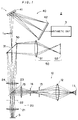
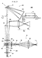
- a microspectroscope including a sample holder, a light source, a beam splitter, a microscopic optical system for imaging observed light from a standard sample or the objective sample and first spectroscopic means for receiving the observed light from the microscopic optical system and separating the observed light into spectral components, as well as first detector means for detecting the spectrum of the observed light is disclosed.
Landscapes
- Physics & Mathematics (AREA)
- Spectroscopy & Molecular Physics (AREA)
- General Physics & Mathematics (AREA)
- Analytical Chemistry (AREA)
- General Health & Medical Sciences (AREA)
- Health & Medical Sciences (AREA)
- Life Sciences & Earth Sciences (AREA)
- Chemical & Material Sciences (AREA)
- Mathematical Physics (AREA)
- Biochemistry (AREA)
- Theoretical Computer Science (AREA)
- Engineering & Computer Science (AREA)
- Immunology (AREA)
- Pathology (AREA)
- Length Measuring Devices By Optical Means (AREA)
- Investigating Or Analysing Materials By Optical Means (AREA)
- Spectrometry And Color Measurement (AREA)
- Microscoopes, Condenser (AREA)
Claims (1)
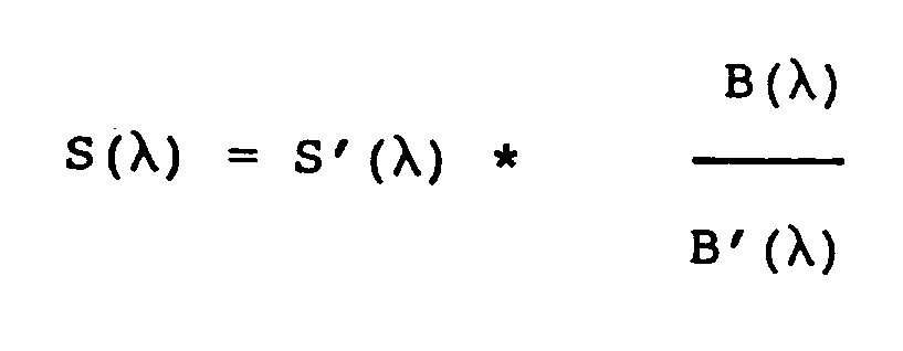
- Mikroskop-Spektralgerät zum Messen des Spektrums B'(λ) einer Standardprobe, die ein bekanntes Spektrum B (λ) besitzt, und des Spektrums S'(λ) einer Objektivprobe (S), die gemessen werden soll und Korrigieren des Spektrums S'(λ) auf der Basis des Spektrums B'(λ), wobei das Mikroskop-Spektralgerät umfaßt:(a) einen Probenhalter zum Halten einer Standardprobe und der Objektivprobe (S);(b) einer Lichtquelle (11) zum Projizieren von Beleuchtungslicht auf den Probenhalter;(c) einem Strahlteiler (23);(d) einem mikroskopisch-optischem System (20) zum Abbilden beobachteten Lichts (LS) von der Standardprobe oder der Objektivprobe (S), die durch den Probenhalter in einer vorgegebenen bilderzeugenden Position gehalten ist;(e) ersten spektroskopischen Mitteln (41) zum Auffangen des erfaßten Lichts (LS) aus dem mikroskopischoptischem System (20) und zum Auftrennen des Lichts (LS) in Spektralkomponenten;(f) und ersten Detektormitteln (42) zum Erfassen des Spektrums des beobachteten Lichts (LS);dadurch gekennzeichnet, daß das mikroskopisch-optische System (20) weiter umfaßt:(g) eine erste Objektivlinse (21), die zwischen einem Strahlteiler (23) und der Objektivprobe (S) angeordnet ist,(h) optische Mittel, die eine zweite Objektivlinse (71), die im wesentlichen die gleichen optischen Charakteristika wie die der ersten Objektivlinse (21) des mikroskopisch-optischen Systems (20) besitzt, und Blendenmitteln (73, 74) umfassen,(i) wobei diese zweite Objektivlinse (71) zwischen der Standardprobe (72) und dem Strahlteiler (23) angeordnet ist,(j) wobei diese Blendenmittel (73, 74) jeweils einen geschlossenen und einen geöffneten Zustand besitzen, so daß entweder Licht reflektiert von der Objektivprobe (S) erfaßt wird, um Daten S'(λ) zu erhalten oder Licht reflektiert von der Standardprobe (72) erfaßt wird, um Daten B'(λ) zu erhalten,(k) wodurch die Korrektur nach der Relation:
Applications Claiming Priority (2)
| Application Number | Priority Date | Filing Date | Title |
|---|---|---|---|
| JP63140733A JPH073365B2 (ja) | 1988-06-08 | 1988-06-08 | 顕微分光装置 |
| JP140733/88 | 1988-06-08 |
Publications (3)
| Publication Number | Publication Date |
|---|---|
| EP0345773A2 EP0345773A2 (de) | 1989-12-13 |
| EP0345773A3 EP0345773A3 (de) | 1991-04-24 |
| EP0345773B1 true EP0345773B1 (de) | 1995-02-22 |
Family
ID=15275442
Family Applications (1)
| Application Number | Title | Priority Date | Filing Date |
|---|---|---|---|
| EP89110378A Expired - Lifetime EP0345773B1 (de) | 1988-06-08 | 1989-06-08 | Mikroskop-Spektralgerät |
Country Status (4)
| Country | Link |
|---|---|
| US (1) | US5048960A (de) |
| EP (1) | EP0345773B1 (de) |
| JP (1) | JPH073365B2 (de) |
| DE (1) | DE68921249T2 (de) |
Families Citing this family (23)
| Publication number | Priority date | Publication date | Assignee | Title |
|---|---|---|---|---|
| US5166080A (en) * | 1991-04-29 | 1992-11-24 | Luxtron Corporation | Techniques for measuring the thickness of a film formed on a substrate |
| US5310260A (en) * | 1990-04-10 | 1994-05-10 | Luxtron Corporation | Non-contact optical techniques for measuring surface conditions |
| US5769540A (en) * | 1990-04-10 | 1998-06-23 | Luxtron Corporation | Non-contact optical techniques for measuring surface conditions |
| US5154512A (en) * | 1990-04-10 | 1992-10-13 | Luxtron Corporation | Non-contact techniques for measuring temperature or radiation-heated objects |
| DE4133125C1 (de) * | 1991-10-05 | 1993-02-18 | Ultrakust Electronic Gmbh, 8375 Gotteszell, De | |
| JP2699753B2 (ja) * | 1992-02-28 | 1998-01-19 | 株式会社島津製作所 | 分光光度計 |
| US5747813A (en) * | 1992-06-16 | 1998-05-05 | Kla-Tencop. Corporation | Broadband microspectro-reflectometer |
| US5486701A (en) * | 1992-06-16 | 1996-01-23 | Prometrix Corporation | Method and apparatus for measuring reflectance in two wavelength bands to enable determination of thin film thickness |
| US5371586A (en) * | 1992-10-09 | 1994-12-06 | Instruments Sa, Inc. | Low aberration diffraction grating system |
| US20070299808A1 (en) * | 1995-05-19 | 2007-12-27 | Cyberfone Technologies, Inc. | Telephone/Transaction Entry Device and System for Entering Transaction Data into Databases |
| JP2853615B2 (ja) * | 1995-08-09 | 1999-02-03 | 富士ゼロックス株式会社 | 電子写真感光体の評価装置および評価方法、電子写真感光体の製造装置および製造方法 |
| DE19548378A1 (de) * | 1995-12-27 | 1997-07-03 | Bran & Luebbe | Verfahren und Gerätekombination zur Herstellung der Vergleichbarkeit von Spektrometermessungen |
| US5701173A (en) * | 1996-02-20 | 1997-12-23 | National Research Council Of Canada | Method and apparatus for reducing the unwanted effects of noise present in a three dimensional color imaging system |
| SG66376A1 (en) * | 1997-07-03 | 1999-07-20 | Inst Of Microlectronics Nation | Multiwavelength imaging and spectroscopic photoemission microscope system |
| US6954275B2 (en) | 2000-08-01 | 2005-10-11 | Boards Of Regents, The University Of Texas System | Methods for high-precision gap and orientation sensing between a transparent template and substrate for imprint lithography |
| US6633391B1 (en) | 2000-11-07 | 2003-10-14 | Applied Materials, Inc | Monitoring of film characteristics during plasma-based semi-conductor processing using optical emission spectroscopy |
| US6603538B1 (en) | 2000-11-21 | 2003-08-05 | Applied Materials, Inc. | Method and apparatus employing optical emission spectroscopy to detect a fault in process conditions of a semiconductor processing system |
| US6917421B1 (en) * | 2001-10-12 | 2005-07-12 | Kla-Tencor Technologies Corp. | Systems and methods for multi-dimensional inspection and/or metrology of a specimen |
| US8349241B2 (en) | 2002-10-04 | 2013-01-08 | Molecular Imprints, Inc. | Method to arrange features on a substrate to replicate features having minimal dimensional variability |
| JP2012063321A (ja) * | 2010-09-17 | 2012-03-29 | Hamamatsu Photonics Kk | 反射率測定装置、反射率測定方法、膜厚測定装置及び膜厚測定方法 |
| US9354114B2 (en) * | 2013-11-19 | 2016-05-31 | Shimadzu Corporation | Spectrophotometer including photodiode array |
| CN103954361B (zh) * | 2014-04-29 | 2016-02-24 | 中国科学院光电研究院 | 一种大孔径多通道空间外差干涉光谱成像方法及光谱仪 |
| CN115372321A (zh) * | 2021-05-18 | 2022-11-22 | 华为技术有限公司 | 一种水质检测系统 |
Citations (1)
| Publication number | Priority date | Publication date | Assignee | Title |
|---|---|---|---|---|
| DE8704679U1 (de) * | 1987-03-30 | 1987-05-27 | Fa. Carl Zeiss, 7920 Heidenheim | Meßgerät für Oberflächen mit bunten Glanzeffekten |
Family Cites Families (9)
| Publication number | Priority date | Publication date | Assignee | Title |
|---|---|---|---|---|
| US2849912A (en) * | 1954-11-20 | 1958-09-02 | Zeiss Carl | Optical arrangement for determining the ratio of two light fluxes |
| US3463592A (en) * | 1964-05-04 | 1969-08-26 | Karl Aron Lennart Akerman | Shifting beam microspectrophotometer with means for selectively varying paths of reference and sample beams through a common optical system |
| US4029419A (en) * | 1975-10-10 | 1977-06-14 | International Business Machines Corporation | Textile color analyzer calibration |
| JPS5519366A (en) * | 1978-07-27 | 1980-02-12 | Sanii Kk | Numericallcontrolled device for opening and closing automatic door |
| GB2113829B (en) * | 1982-01-19 | 1985-07-10 | Philips Electronic Associated | Atomic absorption spectrophotometer |
| JPS5992318A (ja) * | 1982-11-18 | 1984-05-28 | Yamato Scale Co Ltd | 分光測定方法 |
| JPS61217705A (ja) * | 1985-03-22 | 1986-09-27 | Dainippon Screen Mfg Co Ltd | 膜厚測定装置 |
| US4622468A (en) * | 1985-07-15 | 1986-11-11 | Sequoia-Turner Corporation | Fluorescence intensity compensation method and device |
| US4844617A (en) * | 1988-01-20 | 1989-07-04 | Tencor Instruments | Confocal measuring microscope with automatic focusing |
-
1988
- 1988-06-08 JP JP63140733A patent/JPH073365B2/ja not_active Expired - Lifetime
-
1989
- 1989-06-05 US US07/361,406 patent/US5048960A/en not_active Expired - Fee Related
- 1989-06-08 DE DE68921249T patent/DE68921249T2/de not_active Expired - Fee Related
- 1989-06-08 EP EP89110378A patent/EP0345773B1/de not_active Expired - Lifetime
Patent Citations (1)
| Publication number | Priority date | Publication date | Assignee | Title |
|---|---|---|---|---|
| DE8704679U1 (de) * | 1987-03-30 | 1987-05-27 | Fa. Carl Zeiss, 7920 Heidenheim | Meßgerät für Oberflächen mit bunten Glanzeffekten |
Also Published As
| Publication number | Publication date |
|---|---|
| DE68921249T2 (de) | 1995-06-22 |
| DE68921249D1 (de) | 1995-03-30 |
| EP0345773A2 (de) | 1989-12-13 |
| JPH073365B2 (ja) | 1995-01-18 |
| EP0345773A3 (de) | 1991-04-24 |
| JPH01308930A (ja) | 1989-12-13 |
| US5048960A (en) | 1991-09-17 |
Similar Documents
| Publication | Publication Date | Title |
|---|---|---|
| US5048960A (en) | Microspectroscope | |
| US5120966A (en) | Method of and apparatus for measuring film thickness | |
| US5581350A (en) | Method and system for calibrating an ellipsometer | |
| US4984894A (en) | Method of and apparatus for measuring film thickness | |
| EP0800066B1 (de) | Genaue Wellenlängeneichung eines Spektrometers | |
| US5241366A (en) | Thin film thickness monitor | |
| US5910842A (en) | Focused beam spectroscopic ellipsometry method and system | |
| US6734967B1 (en) | Focused beam spectroscopic ellipsometry method and system | |
| US6992779B2 (en) | Interferometer apparatus for both low and high coherence measurement and method thereof | |
| US5771094A (en) | Film measurement system with improved calibration | |
| US6522406B1 (en) | Correcting the system polarization sensitivity of a metrology tool having a rotatable polarizer | |
| US7489399B1 (en) | Spectroscopic multi angle ellipsometry | |
| EP0617255A1 (de) | Verfahren und Vorrichtung zur Messung einer dicken Mikroplatte | |
| US5422703A (en) | Reflected light measuring method and reflected light measuring apparatus for a microscopic photometric system | |
| EP0197199A1 (de) | Vorrichtung und Verfahren zum Messen der Dicke eines Filmes | |
| US7215419B2 (en) | Method and apparatus for position-dependent optical metrology calibration | |
| WO2005121724A2 (en) | Method and apparatus for multi-mode spectral imaging | |
| EP0735350B1 (de) | Spektroskop mit faseroptischer Verzweigung | |
| EP0176826A2 (de) | Verfahren und Vorrichtung für spektrale Zweistrahldurchlässigkeitsmessungen | |
| KR100403440B1 (ko) | 분광분석장치 | |
| EP1593955A2 (de) | Wellenlängenabgestimmte Intensitätsmessung mit einem Oberflächenplasmonenresonanz-Sensor | |
| US6870617B2 (en) | Accurate small-spot spectrometry systems and methods | |
| JPH08122246A (ja) | 分光分析装置 | |
| US4708477A (en) | Photometer | |
| JP4486805B2 (ja) | 分光分析装置 |
Legal Events
| Date | Code | Title | Description |
|---|---|---|---|
| PUAI | Public reference made under article 153(3) epc to a published international application that has entered the european phase |
Free format text: ORIGINAL CODE: 0009012 |
|
| AK | Designated contracting states |
Kind code of ref document: A2 Designated state(s): DE FR GB IT |
|
| PUAL | Search report despatched |
Free format text: ORIGINAL CODE: 0009013 |
|
| AK | Designated contracting states |
Kind code of ref document: A3 Designated state(s): DE FR GB IT |
|
| 17P | Request for examination filed |
Effective date: 19910927 |
|
| 17Q | First examination report despatched |
Effective date: 19920930 |
|
| GRAA | (expected) grant |
Free format text: ORIGINAL CODE: 0009210 |
|
| AK | Designated contracting states |
Kind code of ref document: B1 Designated state(s): DE FR GB IT |
|
| PG25 | Lapsed in a contracting state [announced via postgrant information from national office to epo] |
Ref country code: IT Free format text: LAPSE BECAUSE OF FAILURE TO SUBMIT A TRANSLATION OF THE DESCRIPTION OR TO PAY THE FEE WITHIN THE PRE;WARNING: LAPSES OF ITALIAN PATENTS WITH EFFECTIVE DATE BEFORE 2007 MAY HAVE OCCURRED AT ANY TIME BEFORE 2007. THE CORRECT EFFECTIVE DATE MAY BE DIFFERENT FROM THE ONE RECORDED.SCRIBED TIME-LIMIT Effective date: 19950222 Ref country code: FR Effective date: 19950222 |
|
| REF | Corresponds to: |
Ref document number: 68921249 Country of ref document: DE Date of ref document: 19950330 |
|
| EN | Fr: translation not filed | ||
| PLBE | No opposition filed within time limit |
Free format text: ORIGINAL CODE: 0009261 |
|
| STAA | Information on the status of an ep patent application or granted ep patent |
Free format text: STATUS: NO OPPOSITION FILED WITHIN TIME LIMIT |
|
| 26N | No opposition filed | ||
| PGFP | Annual fee paid to national office [announced via postgrant information from national office to epo] |
Ref country code: GB Payment date: 19980601 Year of fee payment: 10 |
|
| PGFP | Annual fee paid to national office [announced via postgrant information from national office to epo] |
Ref country code: DE Payment date: 19980612 Year of fee payment: 10 |
|
| PG25 | Lapsed in a contracting state [announced via postgrant information from national office to epo] |
Ref country code: GB Free format text: LAPSE BECAUSE OF NON-PAYMENT OF DUE FEES Effective date: 19990608 |
|
| GBPC | Gb: european patent ceased through non-payment of renewal fee |
Effective date: 19990608 |
|
| PG25 | Lapsed in a contracting state [announced via postgrant information from national office to epo] |
Ref country code: DE Free format text: LAPSE BECAUSE OF NON-PAYMENT OF DUE FEES Effective date: 20000503 |