EP0345807A2 - Mémoire de ligne pour conversion de vélocité - Google Patents
Mémoire de ligne pour conversion de vélocité Download PDFInfo
- Publication number
- EP0345807A2 EP0345807A2 EP89110481A EP89110481A EP0345807A2 EP 0345807 A2 EP0345807 A2 EP 0345807A2 EP 89110481 A EP89110481 A EP 89110481A EP 89110481 A EP89110481 A EP 89110481A EP 0345807 A2 EP0345807 A2 EP 0345807A2
- Authority
- EP
- European Patent Office
- Prior art keywords
- write
- read
- reset signal
- address
- shift
- Prior art date
- Legal status (The legal status is an assumption and is not a legal conclusion. Google has not performed a legal analysis and makes no representation as to the accuracy of the status listed.)
- Granted
Links
Images


Classifications
-
- G—PHYSICS
- G11—INFORMATION STORAGE
- G11C—STATIC STORES
- G11C29/00—Checking stores for correct operation ; Subsequent repair; Testing stores during standby or offline operation
-
- G—PHYSICS
- G06—COMPUTING OR CALCULATING; COUNTING
- G06F—ELECTRIC DIGITAL DATA PROCESSING
- G06F5/00—Methods or arrangements for data conversion without changing the order or content of the data handled
- G06F5/06—Methods or arrangements for data conversion without changing the order or content of the data handled for changing the speed of data flow, i.e. speed regularising or timing, e.g. delay lines, FIFO buffers; over- or underrun control therefor
- G06F5/16—Multiplexed systems, i.e. using two or more similar devices which are alternately accessed for enqueue and dequeue operations, e.g. ping-pong buffers
-
- G—PHYSICS
- G11—INFORMATION STORAGE
- G11C—STATIC STORES
- G11C7/00—Arrangements for writing information into, or reading information out from, a digital store
Definitions
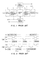
- Memory cell 1 has two memory areas (not illustrated) which contain the same number of memory regions. On this memory cell the write is made alternately in two memory areas and the read-out in the memory area where write is not made. When the ratio of output data D out to input data D in is, for example, two, the read-out speed is twice the write speed. The read-out cycle is therefore repeated twice in one write cycle. In this case, after a write cycle starts at the time when a write address-reset signal WR is entered, the write cycle and two read-out cycles finish at the time when the second read address reset signal RR is entered, and the area to be written and the area to be read out are interchanged.
- shifting reset signals WR′ and RR′ by two clock cycles of input data D in causes a shift quantity of one clock cycle of input data, i.e. two clock cycles of output data, in the data output timing.
- the shift quantity in the data output timing will be equal to a value obtained by subtracting the shift quantity of reset signals WR′ and RR′ from the result of multiplication of the shift quantity by the ratio of output and input data rates (2 in the present case).
Landscapes
- Engineering & Computer Science (AREA)
- Theoretical Computer Science (AREA)
- Physics & Mathematics (AREA)
- General Engineering & Computer Science (AREA)
- General Physics & Mathematics (AREA)
- Communication Control (AREA)
- Image Input (AREA)
- Dram (AREA)
- Static Random-Access Memory (AREA)
Applications Claiming Priority (2)
| Application Number | Priority Date | Filing Date | Title |
|---|---|---|---|
| JP141979/88 | 1988-06-09 | ||
| JP63141979A JPH0642196B2 (ja) | 1988-06-09 | 1988-06-09 | 倍密度走査用ラインメモリ |
Publications (3)
| Publication Number | Publication Date |
|---|---|
| EP0345807A2 true EP0345807A2 (fr) | 1989-12-13 |
| EP0345807A3 EP0345807A3 (fr) | 1991-09-25 |
| EP0345807B1 EP0345807B1 (fr) | 1996-01-03 |
Family
ID=15304574
Family Applications (1)
| Application Number | Title | Priority Date | Filing Date |
|---|---|---|---|
| EP89110481A Expired - Lifetime EP0345807B1 (fr) | 1988-06-09 | 1989-06-09 | Mémoire de ligne pour conversion de vélocité |
Country Status (5)
| Country | Link |
|---|---|
| US (1) | US4945518A (fr) |
| EP (1) | EP0345807B1 (fr) |
| JP (1) | JPH0642196B2 (fr) |
| KR (1) | KR920003754B1 (fr) |
| DE (1) | DE68925307T2 (fr) |
Cited By (1)
| Publication number | Priority date | Publication date | Assignee | Title |
|---|---|---|---|---|
| WO2002014992A1 (fr) * | 2000-08-11 | 2002-02-21 | Advanced Micro Devices, Inc. | Systeme et procede de synchronisation d'un motif d'instructions « passez » et d'initialisation d'une interface de transfert d'horloge dans un systeme a horloges multiples |
Families Citing this family (21)
| Publication number | Priority date | Publication date | Assignee | Title |
|---|---|---|---|---|
| US5086388A (en) * | 1988-03-18 | 1992-02-04 | Hitachi Maxell, Ltd. | Semiconductor serial/parallel-parallel/serial file memory and storage system |
| US5167020A (en) * | 1989-05-25 | 1992-11-24 | The Boeing Company | Serial data transmitter with dual buffers operating separately and having scan and self test modes |
| JPH04188243A (ja) * | 1990-11-21 | 1992-07-06 | Nippon Steel Corp | 記憶装置 |
| JP2999845B2 (ja) * | 1991-04-25 | 2000-01-17 | 沖電気工業株式会社 | シリアルアクセスメモリの倍速コントロール方式 |
| JPH05198163A (ja) * | 1991-10-08 | 1993-08-06 | Mitsubishi Denki Eng Kk | 半導体記憶装置におけるアドレスポインタ |
| GB9208493D0 (en) * | 1992-04-16 | 1992-06-03 | Thomson Consumer Electronics | Dual port video memory |
| JPH06274528A (ja) * | 1993-03-18 | 1994-09-30 | Fujitsu Ltd | ベクトル演算処理装置 |
| JP4018159B2 (ja) * | 1993-06-28 | 2007-12-05 | 株式会社ルネサステクノロジ | 半導体集積回路 |
| JPH0784870A (ja) * | 1993-06-30 | 1995-03-31 | Sanyo Electric Co Ltd | 記憶回路 |
| US5508967A (en) * | 1993-08-09 | 1996-04-16 | Matsushita Electric Industrial Co., Ltd. | Line memory |
| US5479128A (en) * | 1994-03-16 | 1995-12-26 | Industrial Technology Research Institute | Single ram multiple-delay variable delay circuit |
| TW293107B (fr) * | 1994-10-28 | 1996-12-11 | Matsushita Electric Industrial Co Ltd | |
| US5621337A (en) * | 1995-08-30 | 1997-04-15 | National Semiconductor Corporation | Iterative logic circuit |
| JP3789173B2 (ja) * | 1996-07-22 | 2006-06-21 | Necエレクトロニクス株式会社 | 半導体記憶装置及び半導体記憶装置のアクセス方法 |
| KR100602399B1 (ko) * | 1998-02-16 | 2006-07-20 | 소니 가부시끼 가이샤 | 메모리 장치 및 방법 |
| JP2000315147A (ja) * | 1999-04-30 | 2000-11-14 | Oki Electric Ind Co Ltd | データ速度変換回路 |
| JP2001195899A (ja) | 2000-01-06 | 2001-07-19 | Mitsubishi Electric Corp | 半導体記憶装置 |
| KR100372247B1 (ko) * | 2000-05-22 | 2003-02-17 | 삼성전자주식회사 | 프리페치 동작모드를 가지는 반도체 메모리 장치 및 메인데이터 라인수를 줄이기 위한 데이터 전송방법 |
| GB0211173D0 (en) * | 2002-05-16 | 2002-06-26 | Zarlink Semiconductor Inc | Virtual counter for data rate conversion |
| KR20040022102A (ko) * | 2002-09-06 | 2004-03-11 | 위니아만도 주식회사 | 김치저장고의 표시장치 |
| KR102681179B1 (ko) * | 2017-01-23 | 2024-07-04 | 에스케이하이닉스 주식회사 | 메모리 모듈 |
Family Cites Families (6)
| Publication number | Priority date | Publication date | Assignee | Title |
|---|---|---|---|---|
| US3577086A (en) * | 1968-09-30 | 1971-05-04 | Ivan M Kliman | Generator of delayed sequences employing shift register techniques |
| US4287577A (en) * | 1979-09-27 | 1981-09-01 | Communications Satellite Corporation | Interleaved TDMA terrestrial interface buffer |
| JPH07113821B2 (ja) * | 1986-04-21 | 1995-12-06 | 日本テキサス・インスツルメンツ株式会社 | 半導体記憶装置 |
| US4785415A (en) * | 1986-08-29 | 1988-11-15 | Hewlett-Packard Company | Digital data buffer and variable shift register |
| JPH083956B2 (ja) * | 1986-09-18 | 1996-01-17 | 日本テキサス・インスツルメンツ株式会社 | 半導体記憶装置 |
| EP0272869B1 (fr) * | 1986-12-19 | 1993-07-14 | Fujitsu Limited | Dispositif de mémoire à semi-conducteurs à double accès effectuant une opération de lecture à haute vitesse |
-
1988
- 1988-06-09 JP JP63141979A patent/JPH0642196B2/ja not_active Expired - Fee Related
-
1989
- 1989-06-08 US US07/363,276 patent/US4945518A/en not_active Expired - Lifetime
- 1989-06-09 KR KR1019890007942A patent/KR920003754B1/ko not_active Expired
- 1989-06-09 EP EP89110481A patent/EP0345807B1/fr not_active Expired - Lifetime
- 1989-06-09 DE DE68925307T patent/DE68925307T2/de not_active Expired - Fee Related
Cited By (3)
| Publication number | Priority date | Publication date | Assignee | Title |
|---|---|---|---|---|
| WO2002014992A1 (fr) * | 2000-08-11 | 2002-02-21 | Advanced Micro Devices, Inc. | Systeme et procede de synchronisation d'un motif d'instructions « passez » et d'initialisation d'une interface de transfert d'horloge dans un systeme a horloges multiples |
| US6748039B1 (en) | 2000-08-11 | 2004-06-08 | Advanced Micro Devices, Inc. | System and method for synchronizing a skip pattern and initializing a clock forwarding interface in a multiple-clock system |
| KR100804286B1 (ko) * | 2000-08-11 | 2008-02-18 | 어드밴스드 마이크로 디바이시즈, 인코포레이티드 | 다중-클럭 시스템에서 스킵 패턴을 동기화하고 클럭포워딩 인터페이스를 초기화하는 시스템 및 방법 |
Also Published As
| Publication number | Publication date |
|---|---|
| JPH0642196B2 (ja) | 1994-06-01 |
| DE68925307T2 (de) | 1996-05-30 |
| US4945518A (en) | 1990-07-31 |
| EP0345807B1 (fr) | 1996-01-03 |
| KR920003754B1 (ko) | 1992-05-09 |
| KR910001777A (ko) | 1991-01-31 |
| EP0345807A3 (fr) | 1991-09-25 |
| JPH01310433A (ja) | 1989-12-14 |
| DE68925307D1 (de) | 1996-02-15 |
Similar Documents
| Publication | Publication Date | Title |
|---|---|---|
| EP0345807A2 (fr) | Mémoire de ligne pour conversion de vélocité | |
| US4069970A (en) | Data access circuit for a memory array | |
| EP0174845B1 (fr) | Dispositif de mémoire semi-conductrice | |
| GB2232797A (en) | Ram based serial memory with pipelined look-ahead reading | |
| US5146577A (en) | Serial data circuit with randomly-accessed registers of different bit length | |
| US4271483A (en) | Delay circuits | |
| US4713804A (en) | Method and device for converting digital channel multiframes into packet multiframes | |
| EP0520425B1 (fr) | Mémoire à semi-conducteur | |
| EP0209193B1 (fr) | Procédé pour commuter les canaux temporels d'un signal multiplex à division dans le temps et dispositif pour la mise en oeuvre du procédé | |
| US5201058A (en) | Control system for transferring vector data without waiting for transfer end of the previous vector data | |
| US4479180A (en) | Digital memory system utilizing fast and slow address dependent access cycles | |
| EP0057096A2 (fr) | Unité de traitement d'information | |
| GB2115190A (en) | Data word normalisation | |
| US4285047A (en) | Digital adder circuit with a plurality of 1-bit adders and improved carry means | |
| US3993980A (en) | System for hard wiring information into integrated circuit elements | |
| US5412657A (en) | Variable resolution time slot interchange circuit | |
| EP0632458B1 (fr) | Circuit d'emmagasinage de données de sortie parallèle | |
| JPH02141139A (ja) | データ伝送装置 | |
| SU1536366A1 (ru) | Устройство дл ввода-вывода информации | |
| US6252815B1 (en) | First in first out memory circuit | |
| KR0140637B1 (ko) | 개선된 시프트 레지스터 | |
| SU822292A1 (ru) | Посто нное запоминающее устройство | |
| SU1026163A1 (ru) | Устройство дл управлени записью и считыванием информации | |
| JPS61288636A (ja) | フレ−ム変換回路 | |
| JP2613963B2 (ja) | データ入出力装置 |
Legal Events
| Date | Code | Title | Description |
|---|---|---|---|
| PUAI | Public reference made under article 153(3) epc to a published international application that has entered the european phase |
Free format text: ORIGINAL CODE: 0009012 |
|
| 17P | Request for examination filed |
Effective date: 19890609 |
|
| AK | Designated contracting states |
Kind code of ref document: A2 Designated state(s): DE FR GB |
|
| PUAL | Search report despatched |
Free format text: ORIGINAL CODE: 0009013 |
|
| AK | Designated contracting states |
Kind code of ref document: A3 Designated state(s): DE FR GB |
|
| 17Q | First examination report despatched |
Effective date: 19940321 |
|
| GRAA | (expected) grant |
Free format text: ORIGINAL CODE: 0009210 |
|
| AK | Designated contracting states |
Kind code of ref document: B1 Designated state(s): DE FR GB |
|
| REF | Corresponds to: |
Ref document number: 68925307 Country of ref document: DE Date of ref document: 19960215 |
|
| ET | Fr: translation filed | ||
| PLBE | No opposition filed within time limit |
Free format text: ORIGINAL CODE: 0009261 |
|
| STAA | Information on the status of an ep patent application or granted ep patent |
Free format text: STATUS: NO OPPOSITION FILED WITHIN TIME LIMIT |
|
| 26N | No opposition filed | ||
| PGFP | Annual fee paid to national office [announced via postgrant information from national office to epo] |
Ref country code: GB Payment date: 19970602 Year of fee payment: 9 |
|
| PGFP | Annual fee paid to national office [announced via postgrant information from national office to epo] |
Ref country code: FR Payment date: 19970610 Year of fee payment: 9 |
|
| PG25 | Lapsed in a contracting state [announced via postgrant information from national office to epo] |
Ref country code: GB Free format text: LAPSE BECAUSE OF NON-PAYMENT OF DUE FEES Effective date: 19980609 |
|
| GBPC | Gb: european patent ceased through non-payment of renewal fee |
Effective date: 19980609 |
|
| PG25 | Lapsed in a contracting state [announced via postgrant information from national office to epo] |
Ref country code: FR Free format text: LAPSE BECAUSE OF NON-PAYMENT OF DUE FEES Effective date: 19990226 |
|
| REG | Reference to a national code |
Ref country code: FR Ref legal event code: ST |
|
| PGFP | Annual fee paid to national office [announced via postgrant information from national office to epo] |
Ref country code: DE Payment date: 20060601 Year of fee payment: 18 |
|
| PG25 | Lapsed in a contracting state [announced via postgrant information from national office to epo] |
Ref country code: DE Free format text: LAPSE BECAUSE OF NON-PAYMENT OF DUE FEES Effective date: 20080101 |